Nanoscale femtosecond spectroscopy for material science and ...
Nanoscale femtosecond spectroscopy for material science and ...
Nanoscale femtosecond spectroscopy for material science and ...

You also want an ePaper? Increase the reach of your titles
YUMPU automatically turns print PDFs into web optimized ePapers that Google loves.
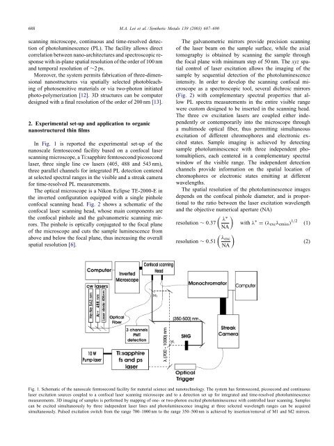
688 M.A. Loi et al. / Synthetic Metals 139 (2003) 687–690scanning microscope, continuous <strong>and</strong> time-resolved detectionof photoluminescence (PL). The facility allows directcorrelation between nano-architectures <strong>and</strong> spectroscopic responsewith in-plane spatial resolution of the order of 100 nm<strong>and</strong> temporal resolution of ∼2 ps.Moreover, the system permits fabrication of three-dimensionalnanostructures via spatially selected photobleachingof photosensitive <strong>material</strong>s or via two-photon initiatedphoto-polymerization [12]. 3D structures can be computerdesigned with a final resolution of the order of 200 nm [13].2. Experimental set-up <strong>and</strong> application to organicnanostructured thin filmsIn Fig. 1 is reported the experimental set-up of thenanoscale <strong>femtosecond</strong> facility based on a confocal laserscanning microscope, a Ti:sapphire <strong>femtosecond</strong>/picosecondlaser, three single line cw lasers (405, 488 <strong>and</strong> 543 nm),three parallel channels <strong>for</strong> integrated PL detection centeredat selected spectral ranges in the visible <strong>and</strong> a streak camera<strong>for</strong> time-resolved PL measurements.The optical microscope is a Nikon Eclipse TE-2000-E inthe inverted configuration equipped with a single pinholeconfocal scanning head. Fig. 2 shows a schematic of theconfocal laser scanning head, whose main components arethe confocal pinhole <strong>and</strong> the galvanometric scanning mirrors.The pinhole is optically conjugated to the focal planeof the microscope <strong>and</strong> cuts the sample luminescence fromabove <strong>and</strong> below the focal plane, thus increasing the overallspatial resolution [6].The galvanometric mirrors provide precision scanningof the laser beam on the sample surface, while the axialtomography is obtained by scanning the sample throughthe focal plane with minimum step of 50 nm. The xyz spatialcontrol of laser excitation allows the imaging of thesample by sequential detection of the photoluminescenceintensity. In order to develop the scanning confocal microscopeas a spectroscopic tool, several dichroic mirrors(Fig. 2) with complementary spectral properties that allowPL spectra measurements in the entire visible rangewere custom designed to be inserted in the scanning head.The three cw excitation lasers are coupled either independentlyor contemporarily into the microscope througha multimode optical fiber, thus permitting simultaneousexcitation of different chromophores <strong>and</strong> electronic excitedstates. Sample imaging is achieved by detectingsample photoluminescence with three independent photomultipliers,each centered in a complementary spectralwindow of the visible range. The independent detectionchannels provide in<strong>for</strong>mation on the spatial location ofchromophores or electronic states emitting at differentwavelengths.The spatial resolution of the photoluminescence imagesdepends on the confocal pinhole diameter, <strong>and</strong> is proportionalto the ratio between the laser excitation wavelength<strong>and</strong> the objective numerical aperture (NA)( λ∗)resolution ∼ 0.37 with λ ∗ = (λ exc λ emiss ) 1/2 (1)NA( )λexcresolution ∼ 0.51(2)NAFig. 1. Schematic of the nanoscale <strong>femtosecond</strong> facility <strong>for</strong> <strong>material</strong> <strong>science</strong> <strong>and</strong> nanotechnology. The system has <strong>femtosecond</strong>, picosecond <strong>and</strong> continuouslaser excitation sources coupled to a confocal laser scanning microscope <strong>and</strong> to a detection set up <strong>for</strong> integrated <strong>and</strong> time-resolved photoluminescencemeasurements. 3D imaging of samples is per<strong>for</strong>med by mapping of one- or two-photon excited photoluminescence with controlled laser scanning. Samplescan be excited simultaneously by three independent laser lines <strong>and</strong> photoluminescence imaging at three selected wavelength ranges can be acquiredsimultaneously. Pulsed excitation switch from the range 700–1000 nm to the range 350–500 nm is achieved by insertion/removal of M1 <strong>and</strong> M2 mirrors.