Nanoscale femtosecond spectroscopy for material science and ...
Nanoscale femtosecond spectroscopy for material science and ...
Nanoscale femtosecond spectroscopy for material science and ...

You also want an ePaper? Increase the reach of your titles
YUMPU automatically turns print PDFs into web optimized ePapers that Google loves.
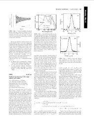
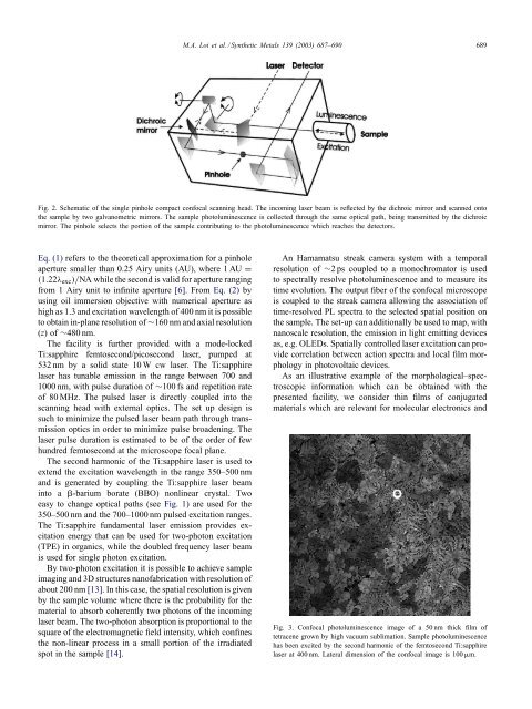
M.A. Loi et al. / Synthetic Metals 139 (2003) 687–690 689Fig. 2. Schematic of the single pinhole compact confocal scanning head. The incoming laser beam is reflected by the dichroic mirror <strong>and</strong> scanned ontothe sample by two galvanometric mirrors. The sample photoluminescence is collected through the same optical path, being transmitted by the dichroicmirror. The pinhole selects the portion of the sample contributing to the photoluminescence which reaches the detectors.Eq. (1) refers to the theoretical approximation <strong>for</strong> a pinholeaperture smaller than 0.25 Airy units (AU), where 1 AU =(1.22λ exc )/NA while the second is valid <strong>for</strong> aperture rangingfrom 1 Airy unit to infinite aperture [6]. From Eq. (2) byusing oil immersion objective with numerical aperture ashigh as 1.3 <strong>and</strong> excitation wavelength of 400 nm it is possibleto obtain in-plane resolution of ∼160 nm <strong>and</strong> axial resolution(z) of∼480 nm.The facility is further provided with a mode-lockedTi:sapphire <strong>femtosecond</strong>/picosecond laser, pumped at532 nm by a solid state 10 W cw laser. The Ti:sapphirelaser has tunable emission in the range between 700 <strong>and</strong>1000 nm, with pulse duration of ∼100 fs <strong>and</strong> repetition rateof 80 MHz. The pulsed laser is directly coupled into thescanning head with external optics. The set up design issuch to minimize the pulsed laser beam path through transmissionoptics in order to minimize pulse broadening. Thelaser pulse duration is estimated to be of the order of fewhundred <strong>femtosecond</strong> at the microscope focal plane.The second harmonic of the Ti:sapphire laser is used toextend the excitation wavelength in the range 350–500 nm<strong>and</strong> is generated by coupling the Ti:sapphire laser beaminto a -barium borate (BBO) nonlinear crystal. Twoeasy to change optical paths (see Fig. 1) are used <strong>for</strong> the350–500 nm <strong>and</strong> the 700–1000 nm pulsed excitation ranges.The Ti:sapphire fundamental laser emission provides excitationenergy that can be used <strong>for</strong> two-photon excitation(TPE) in organics, while the doubled frequency laser beamis used <strong>for</strong> single photon excitation.By two-photon excitation it is possible to achieve sampleimaging <strong>and</strong> 3D structures nanofabrication with resolution ofabout 200 nm [13]. In this case, the spatial resolution is givenby the sample volume where there is the probability <strong>for</strong> the<strong>material</strong> to absorb coherently two photons of the incominglaser beam. The two-photon absorption is proportional to thesquare of the electromagnetic field intensity, which confinesthe non-linear process in a small portion of the irradiatedspot in the sample [14].An Hamamatsu streak camera system with a temporalresolution of ∼2 ps coupled to a monochromator is usedto spectrally resolve photoluminescence <strong>and</strong> to measure itstime evolution. The output fiber of the confocal microscopeis coupled to the streak camera allowing the association oftime-resolved PL spectra to the selected spatial position onthe sample. The set-up can additionally be used to map, withnanoscale resolution, the emission in light emitting devicesas, e.g. OLEDs. Spatially controlled laser excitation can providecorrelation between action spectra <strong>and</strong> local film morphologyin photovoltaic devices.As an illustrative example of the morphological–spectroscopicin<strong>for</strong>mation which can be obtained with thepresented facility, we consider thin films of conjugated<strong>material</strong>s which are relevant <strong>for</strong> molecular electronics <strong>and</strong>Fig. 3. Confocal photoluminescence image of a 50 nm thick film oftetracene grown by high vacuum sublimation. Sample photoluminescencehas been excited by the second harmonic of the <strong>femtosecond</strong> Ti:sapphirelaser at 400 nm. Lateral dimension of the confocal image is 100 m.