- Page 2 and 3:
Passive, Active,and DigitalFilters
- Page 4 and 5:
The Circuits and Filters HandbookTh
- Page 6 and 7:
ContentsPreface ...................
- Page 10:
PrefaceAs circuit complexity contin
- Page 14 and 15:
ContributorsPhillip E. AllenSchool
- Page 16 and 17:
IPassive FiltersWai-Kai ChenUnivers
- Page 18 and 19:
1General Characteristicsof FiltersA
- Page 20 and 21:
General Characteristics of Filters
- Page 22 and 23:
General Characteristics of Filters
- Page 24 and 25:
General Characteristics of Filters
- Page 26 and 27:
General Characteristics of Filters
- Page 29 and 30:
1-12 Passive, Active, and Digital F
- Page 31 and 32:
1-14 Passive, Active, and Digital F
- Page 34 and 35:
General Characteristics of Filters
- Page 38 and 39:
General Characteristics of Filters
- Page 40 and 41:
General Characteristics of Filters
- Page 42 and 43:
General Characteristics of Filters
- Page 44 and 45:
General Characteristics of Filters
- Page 46:
General Characteristics of Filters
- Page 49 and 50:
2-2 Passive, Active, and Digital Fi
- Page 51 and 52:
2-4 Passive, Active, and Digital Fi
- Page 53 and 54:
2-6 Passive, Active, and Digital Fi
- Page 56:
Approximation 2-9K(ω)Large nSmall
- Page 60 and 61:
Approximation 2-132π21φ = cos -1
- Page 62:
Approximation 2-15This result is us
- Page 66 and 67:
Approximation 2-19Butterworth; put
- Page 68 and 69:
Approximation 2-21This however impl
- Page 70 and 71:
Approximation 2-23TABLE 2.3 Bessel
- Page 72 and 73:
Approximation 2-25R mn (ω)b + εbb
- Page 74 and 75:
Approximation 2-27is a measure of t
- Page 76 and 77:
Approximation 2-29Recall, now, the
- Page 78 and 79:
Approximation 2-31TABLE 2.4 Zeros o
- Page 80:
Approximation 2-33References1. A. M
- Page 83 and 84:
3-2 Passive, Active, and Digital Fi
- Page 85 and 86:
3-4 Passive, Active, and Digital Fi
- Page 87 and 88:
3-6 Passive, Active, and Digital Fi
- Page 89 and 90:
3-8 Passive, Active, and Digital Fi
- Page 91 and 92:
3-10 Passive, Active, and Digital F
- Page 93 and 94:
3-12 Passive, Active, and Digital F
- Page 96 and 97:
4Sensitivityand SelectivityIgor M.
- Page 98 and 99:
Sensitivity and Selectivity 4-34.3
- Page 100 and 101:
Sensitivity and Selectivity 4-5Beca
- Page 102 and 103:
Sensitivity and Selectivity 4-7Simi
- Page 104 and 105:
Sensitivity and Selectivity 4-9comp
- Page 106 and 107:
Sensitivity and Selectivity 4-11In
- Page 108 and 109:
Sensitivity and Selectivity 4-13and
- Page 110 and 111:
Sensitivity and Selectivity 4-154.8
- Page 112 and 113:
Sensitivity and Selectivity 4-17cha
- Page 114 and 115:
Sensitivity and Selectivity 4-19Tak
- Page 116 and 117:
Sensitivity and Selectivity 4-21I p
- Page 118 and 119:
Sensitivity and Selectivity 4-23Att
- Page 120 and 121:
Sensitivity and Selectivity 4-25 In
- Page 122 and 123:
Sensitivity and Selectivity 4-27the
- Page 124 and 125:
Sensitivity and Selectivity 4-29is
- Page 126 and 127:
Sensitivity and Selectivity 4-311.
- Page 128 and 129:
5Passive Immittancesand Positive-Re
- Page 130 and 131:
Passive Immittances and Positive-Re
- Page 132 and 133:
Passive Immittances and Positive-Re
- Page 134 and 135:
Passive Immittances and Positive-Re
- Page 136 and 137:
6Passive CascadeSynthesisWai-Kai Ch
- Page 138 and 139:
Passive Cascade Synthesis 6-3not gr
- Page 140 and 141:
Passive Cascade Synthesis 6-5degree
- Page 142 and 143:
Passive Cascade Synthesis 6-7M < 0L
- Page 144 and 145:
Passive Cascade Synthesis 6-9LN AFI
- Page 146 and 147:
Passive Cascade Synthesis 6-11ζCN
- Page 148 and 149:
Passive Cascade Synthesis 6-13the d
- Page 150 and 151:
Passive Cascade Synthesis 6-15The e
- Page 152 and 153:
7Synthesis of LCM andRC One-Port Ne
- Page 154 and 155:
Synthesis of LCM and RC One-Port Ne
- Page 156 and 157:
Synthesis of LCM and RC One-Port Ne
- Page 158 and 159:
Synthesis of LCM and RC One-Port Ne
- Page 160 and 161:
Synthesis of LCM and RC One-Port Ne
- Page 162:
Synthesis of LCM and RC One-Port Ne
- Page 165 and 166:
8-2 Passive, Active, and Digital Fi
- Page 167 and 168:
8-4 Passive, Active, and Digital Fi
- Page 169 and 170:
8-6 Passive, Active, and Digital Fi
- Page 171 and 172:
8-8 Passive, Active, and Digital Fi
- Page 173 and 174:
8-10 Passive, Active, and Digital F
- Page 175 and 176:
8-12 Passive, Active, and Digital F
- Page 177 and 178:
8-14 Passive, Active, and Digital F
- Page 179 and 180:
8-16 Passive, Active, and Digital F
- Page 181 and 182:
9-2 Passive, Active, and Digital Fi
- Page 183 and 184:
9-4 Passive, Active, and Digital Fi
- Page 185 and 186:
9-6 Passive, Active, and Digital Fi
- Page 187 and 188:
V g-V g-9-8 Passive, Active, and Di
- Page 189 and 190:
9-10 Passive, Active, and Digital F
- Page 191 and 192:
9-12 Passive, Active, and Digital F
- Page 194 and 195:
10Design of BroadbandMatching Netwo
- Page 196 and 197:
Design of Broadband Matching Networ
- Page 198 and 199:
Design of Broadband Matching Networ
- Page 200 and 201:
Design of Broadband Matching Networ
- Page 202 and 203:
Design of Broadband Matching Networ
- Page 204 and 205:
Design of Broadband Matching Networ
- Page 206 and 207:
Design of Broadband Matching Networ
- Page 208 and 209:
Design of Broadband Matching Networ
- Page 210 and 211:
Design of Broadband Matching Networ
- Page 212 and 213:
Design of Broadband Matching Networ
- Page 214 and 215:
Design of Broadband Matching Networ
- Page 216 and 217:
Design of Broadband Matching Networ
- Page 218 and 219:
Design of Broadband Matching Networ
- Page 220 and 221:
Design of Broadband Matching Networ
- Page 222 and 223:
Design of Broadband Matching Networ
- Page 224 and 225:
IIActive FiltersWai-Kai ChenUnivers
- Page 226 and 227:
11Low-Gain Active FiltersPhillip E.
- Page 228 and 229:
Low-Gain Active Filters 11-3The dam
- Page 230 and 231:
Low-Gain Active Filters 11-5at a fr
- Page 232 and 233:
Low-Gain Active Filters 11-7+RK++CK
- Page 234 and 235:
Low-Gain Active Filters 11-9R 2+R 1
- Page 236 and 237:
Low-Gain Active Filters 11-11For th
- Page 238 and 239:
Low-Gain Active Filters 11-13The se
- Page 240 and 241:
Low-Gain Active Filters 11-15Y 1H22
- Page 242 and 243:
Low-Gain Active Filters 11-17R 2+R
- Page 244 and 245:
Low-Gain Active Filters 11-19To con
- Page 246 and 247:
Low-Gain Active Filters 11-21+10k 1
- Page 248 and 249:
Low-Gain Active Filters 11-23TABLE
- Page 250 and 251:
Low-Gain Active Filters 11-25The ph
- Page 252 and 253:
Low-Gain Active Filters 11-27TABLE
- Page 254 and 255:
Low-Gain Active Filters 11-29I n1E
- Page 256 and 257:
Low-Gain Active Filters 11-3150 nVS
- Page 258 and 259:
12Single-AmplifierMultiple-Feedback
- Page 260 and 261:
Single-Amplifier Multiple-Feedback
- Page 262 and 263:
Single-Amplifier Multiple-Feedback
- Page 264 and 265:
Single-Amplifier Multiple-Feedback
- Page 266 and 267:
Single-Amplifier Multiple-Feedback
- Page 268 and 269:
Single-Amplifier Multiple-Feedback
- Page 270:
Single-Amplifier Multiple-Feedback
- Page 273 and 274:
13-2 Passive, Active, and Digital F
- Page 275 and 276:
13-4 Passive, Active, and Digital F
- Page 277 and 278:
13-6 Passive, Active, and Digital F
- Page 279 and 280:
13-8 Passive, Active, and Digital F
- Page 281 and 282:
13-10 Passive, Active, and Digital
- Page 283 and 284:
13-12 Passive, Active, and Digital
- Page 285 and 286:
13-14 Passive, Active, and Digital
- Page 287 and 288:
13-16 Passive, Active, and Digital
- Page 289 and 290:
13-18 Passive, Active, and Digital
- Page 291 and 292:
13-20 Passive, Active, and Digital
- Page 293 and 294:
13-22 Passive, Active, and Digital
- Page 295 and 296:
13-24 Passive, Active, and Digital
- Page 297 and 298:
13-26 Passive, Active, and Digital
- Page 300 and 301:
14The CurrentGeneralizedImmittance
- Page 302 and 303:
The Current Generalized Immittance
- Page 304 and 305:
The Current Generalized Immittance
- Page 306 and 307:
The Current Generalized Immittance
- Page 308 and 309:
The Current Generalized Immittance
- Page 310 and 311:
The Current Generalized Immittance
- Page 312 and 313:
The Current Generalized Immittance
- Page 314 and 315:
The Current Generalized Immittance
- Page 316 and 317:
The Current Generalized Immittance
- Page 318 and 319:
The Current Generalized Immittance
- Page 320 and 321:
15High-Order FiltersRolf SchaumannP
- Page 322 and 323:
High-Order Filters 15-3V inV o2V oi
- Page 324 and 325:
High-Order Filters 15-5Choosing the
- Page 326 and 327:
High-Order Filters 15-7where we def
- Page 328 and 329:
High-Order Filters 15-9where we int
- Page 330 and 331:
High-Order Filters 15-11where s is
- Page 332 and 333:
High-Order Filters 15-1315.4.1 Sign
- Page 334 and 335:
High-Order Filters 15-15Ri2R 4V oR
- Page 336 and 337: High-Order Filters 15-17Notice that
- Page 338 and 339: High-Order Filters 15-19v i g i(α
- Page 340 and 341: High-Order Filters 15-21TABLE 15.1
- Page 342 and 343: High-Order Filters 15-23R a1 ¼ ^C
- Page 344 and 345: High-Order Filters 15-25I 1 1V 1 sk
- Page 346 and 347: High-Order Filters 15-27664154015.2
- Page 348 and 349: 16Continuous-TimeIntegrated Filters
- Page 350 and 351: Continuous-Time Integrated Filters
- Page 352 and 353: Continuous-Time Integrated Filters
- Page 354 and 355: Continuous-Time Integrated Filters
- Page 356 and 357: Continuous-Time Integrated Filters
- Page 358 and 359: Continuous-Time Integrated Filters
- Page 360 and 361: Continuous-Time Integrated Filters
- Page 362 and 363: Continuous-Time Integrated Filters
- Page 364 and 365: Continuous-Time Integrated Filters
- Page 366 and 367: Continuous-Time Integrated Filters
- Page 368 and 369: Continuous-Time Integrated Filters
- Page 370 and 371: Continuous-Time Integrated Filters
- Page 372 and 373: Continuous-Time Integrated Filters
- Page 374 and 375: Continuous-Time Integrated Filters
- Page 376 and 377: Continuous-Time Integrated Filters
- Page 378 and 379: Continuous-Time Integrated Filters
- Page 380 and 381: Continuous-Time Integrated Filters
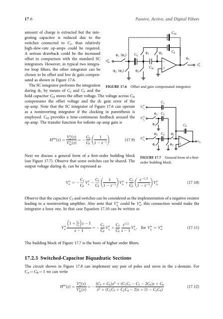
- Page 382 and 383: 17Switched-CapacitorFiltersJose Sil
- Page 384 and 385: Switched-Capacitor Filters 17-3C SC
- Page 388 and 389: Switched-Capacitor Filters 17-7φ 2
- Page 390 and 391: Switched-Capacitor Filters 17-9A 3
- Page 392 and 393: Switched-Capacitor Filters 17-11whe
- Page 394 and 395: Switched-Capacitor Filters 17-1317.
- Page 396 and 397: Switched-Capacitor Filters 17-15C i
- Page 398 and 399: Switched-Capacitor Filters 17-1717.
- Page 400 and 401: Switched-Capacitor Filters 17-19The
- Page 402 and 403: Switched-Capacitor Filters 17-21Dur
- Page 404 and 405: Switched-Capacitor Filters 17-23sig
- Page 406 and 407: Switched-Capacitor Filters 17-25C 1
- Page 408 and 409: Switched-Capacitor Filters 17-27φC
- Page 410 and 411: Switched-Capacitor Filters 17-29for
- Page 412 and 413: Switched-Capacitor Filters 17-31If
- Page 414 and 415: Switched-Capacitor Filters 17-33FIG
- Page 416 and 417: Switched-Capacitor Filters 17-35CH1
- Page 418 and 419: IIIDigital FiltersRashid AnsariUniv
- Page 420 and 421: 18FIR FiltersM. H. ErNanyang Techno
- Page 422 and 423: FIR Filters 18-3Consequently,tan (v
- Page 424 and 425: FIR Filters 18-5TABLE 18.1Frequency
- Page 426 and 427: FIR Filters 18-7H d (e jω )1To und
- Page 428 and 429: FIR Filters 18-90-10-20Amplitude re
- Page 430 and 431: FIR Filters 18-110-5-10Amplitude re
- Page 432 and 433: FIR Filters 18-130-20Amplitude resp
- Page 434 and 435: FIR Filters 18-15TABLE 18.2Spectral
- Page 436 and 437:
FIR Filters 18-17If it were possibl
- Page 438 and 439:
FIR Filters 18-19The alternation th
- Page 440 and 441:
FIR Filters 18-21respectively, and
- Page 442 and 443:
FIR Filters 18-23Rejection of super
- Page 444 and 445:
FIR Filters 18-25The selective step
- Page 446 and 447:
FIR Filters 18-27TABLE 18.4 Impulse
- Page 448 and 449:
FIR Filters 18-29selective step-by-
- Page 450 and 451:
FIR Filters 18-31Odd filter lengthM
- Page 452 and 453:
FIR Filters 18-33and1a 1 ¼ ~c 02 ~
- Page 454 and 455:
FIR Filters 18-35a useful property
- Page 456 and 457:
FIR Filters 18-37with the number of
- Page 458 and 459:
FIR Filters 18-39F(z L )z −LN F /
- Page 460 and 461:
FIR Filters 18-411F(Lω)G 1 (ω)0 0
- Page 462 and 463:
FIR Filters 18-43TABLE 18.11Algorit
- Page 464 and 465:
FIR Filters 18-451N ove ¼ N optL
- Page 466 and 467:
FIR Filters 18-47TABLE 18.13 Implem
- Page 468 and 469:
FIR Filters 18-494. If r ¼ R, then
- Page 470 and 471:
FIR Filters 18-51In this case, the
- Page 472 and 473:
FIR Filters 18-53Estimated orders11
- Page 474 and 475:
FIR Filters 18-550Amplitude (db)−
- Page 476 and 477:
FIR Filters 18-57In the above, the
- Page 478 and 479:
FIR Filters 18-59TABLE 18.15Data fo
- Page 480:
FIR Filters 18-614. Y. C. Lim and Y
- Page 483 and 484:
19-2 Passive, Active, and Digital F
- Page 485 and 486:
19-4 Passive, Active, and Digital F
- Page 487 and 488:
19-6 Passive, Active, and Digital F
- Page 489 and 490:
19-8 Passive, Active, and Digital F
- Page 491 and 492:
19-10 Passive, Active, and Digital
- Page 493 and 494:
19-12 Passive, Active, and Digital
- Page 495 and 496:
19-14 Passive, Active, and Digital
- Page 497 and 498:
19-16 Passive, Active, and Digital
- Page 499 and 500:
19-18 Passive, Active, and Digital
- Page 501 and 502:
19-20 Passive, Active, and Digital
- Page 503 and 504:
19-22 Passive, Active, and Digital
- Page 505 and 506:
19-24 Passive, Active, and Digital
- Page 507 and 508:
19-26 Passive, Active, and Digital
- Page 509 and 510:
19-28 Passive, Active, and Digital
- Page 511 and 512:
19-30 Passive, Active, and Digital
- Page 513 and 514:
19-32 Passive, Active, and Digital
- Page 515 and 516:
19-34 Passive, Active, and Digital
- Page 517 and 518:
19-36 Passive, Active, and Digital
- Page 519 and 520:
19-38 Passive, Active, and Digital
- Page 521 and 522:
19-40 Passive, Active, and Digital
- Page 523 and 524:
19-42 Passive, Active, and Digital
- Page 525 and 526:
19-44 Passive, Active, and Digital
- Page 528 and 529:
20Finite WordlengthEffectsBruce W.
- Page 530 and 531:
Finite Wordlength Effects 20-3the q
- Page 532 and 533:
Finite Wordlength Effects 20-5From
- Page 534 and 535:
Finite Wordlength Effects 20-7In ge
- Page 536 and 537:
Finite Wordlength Effects 20-9To ob
- Page 538 and 539:
Finite Wordlength Effects 20-11Howe
- Page 540 and 541:
Finite Wordlength Effects 20-13wher
- Page 542 and 543:
Finite Wordlength Effects 20-15 y(4
- Page 544 and 545:
Finite Wordlength Effects 20-17j1.0
- Page 546:
Finite Wordlength Effects 20-1921.
- Page 549 and 550:
21-2 Passive, Active, and Digital F
- Page 551 and 552:
21-4 Passive, Active, and Digital F
- Page 553 and 554:
21-6 Passive, Active, and Digital F
- Page 555 and 556:
21-8 Passive, Active, and Digital F
- Page 557 and 558:
21-10 Passive, Active, and Digital
- Page 559 and 560:
21-12 Passive, Active, and Digital
- Page 561 and 562:
21-14 Passive, Active, and Digital
- Page 563 and 564:
21-16 Passive, Active, and Digital
- Page 565 and 566:
22-2 Passive, Active, and Digital F
- Page 567 and 568:
22-4 Passive, Active, and Digital F
- Page 569 and 570:
22-6 Passive, Active, and Digital F
- Page 571 and 572:
22-8 Passive, Active, and Digital F
- Page 573 and 574:
22-10 Passive, Active, and Digital
- Page 575 and 576:
22-12 Passive, Active, and Digital
- Page 577 and 578:
22-14 Passive, Active, and Digital
- Page 579 and 580:
22-16 Passive, Active, and Digital
- Page 581 and 582:
22-18 Passive, Active, and Digital
- Page 583 and 584:
22-20 Passive, Active, and Digital
- Page 585 and 586:
22-22 Passive, Active, and Digital
- Page 587 and 588:
22-24 Passive, Active, and Digital
- Page 589 and 590:
22-26 Passive, Active, and Digital
- Page 591 and 592:
22-28 Passive, Active, and Digital
- Page 594 and 595:
23Two-DimensionalIIR FiltersA. G. C
- Page 596 and 597:
Two-Dimensional IIR Filters 23-323.
- Page 598 and 599:
Two-Dimensional IIR Filters 23-5a 1
- Page 600 and 601:
Two-Dimensional IIR Filters 23-7x(n
- Page 602 and 603:
Two-Dimensional IIR Filters 23-9+π
- Page 604 and 605:
Two-Dimensional IIR Filters 23-11TA
- Page 606 and 607:
Two-Dimensional IIR Filters 23-13wh
- Page 608 and 609:
Two-Dimensional IIR Filters 23-15ω
- Page 610 and 611:
Two-Dimensional IIR Filters 23-17x
- Page 612 and 613:
Two-Dimensional IIR Filters 23-19St
- Page 614 and 615:
Two-Dimensional IIR Filters 23-21In
- Page 616 and 617:
Two-Dimensional IIR Filters 23-23an
- Page 618 and 619:
Two-Dimensional IIR Filters 23-25-1
- Page 620 and 621:
Two-Dimensional IIR Filters 23-2711
- Page 622 and 623:
Two-Dimensional IIR Filters 23-29is
- Page 624 and 625:
Two-Dimensional IIR Filters 23-31wh
- Page 626 and 627:
Two-Dimensional IIR Filters 23-33Co
- Page 628 and 629:
Two-Dimensional IIR Filters 23-35In
- Page 630 and 631:
Two-Dimensional IIR Filters 23-37f
- Page 632 and 633:
Two-Dimensional IIR Filters 23-39If
- Page 634 and 635:
Two-Dimensional IIR Filters 23-41TA
- Page 636 and 637:
Two-Dimensional IIR Filters 23-43f
- Page 638 and 639:
Two-Dimensional IIR Filters 23-45St
- Page 640 and 641:
Two-Dimensional IIR Filters 23-47wh
- Page 642 and 643:
241-D MultirateFilter BanksNick G.
- Page 644 and 645:
1-D Multirate Filter Banks 24-324.2
- Page 646 and 647:
1-D Multirate Filter Banks 24-5Subs
- Page 648 and 649:
1-D Multirate Filter Banks 24-7y 00
- Page 650 and 651:
1-D Multirate Filter Banks 24-9Haar
- Page 652 and 653:
1-D Multirate Filter Banks 24-11H k
- Page 654 and 655:
1-D Multirate Filter Banks 24-13Now
- Page 656 and 657:
1-D Multirate Filter Banks 24-1510h
- Page 658 and 659:
1-D Multirate Filter Banks 24-17Equ
- Page 660 and 661:
1-D Multirate Filter Banks 24-191Da
- Page 662 and 663:
1-D Multirate Filter Banks 24-211An
- Page 664 and 665:
1-D Multirate Filter Banks 24-231Ne
- Page 666 and 667:
1-D Multirate Filter Banks 24-25dur
- Page 668 and 669:
1-D Multirate Filter Banks 24-27Rec
- Page 670 and 671:
1-D Multirate Filter Banks 24-29pre
- Page 672 and 673:
1-D Multirate Filter Banks 24-31The
- Page 674 and 675:
1-D Multirate Filter Banks 24-332An
- Page 676 and 677:
1-D Multirate Filter Banks 24-352.
- Page 678 and 679:
1-D Multirate Filter Banks 24-3724.
- Page 680 and 681:
1-D Multirate Filter Banks 24-39by
- Page 682 and 683:
1-D Multirate Filter Banks 24-41x0
- Page 684 and 685:
1-D Multirate Filter Banks 24-43pri
- Page 686 and 687:
1-D Multirate Filter Banks 24-45The
- Page 688 and 689:
1-D Multirate Filter Banks 24-47Two
- Page 690 and 691:
1-D Multirate Filter Banks 24-49" #
- Page 692 and 693:
1-D Multirate Filter Banks 24-51Tre
- Page 694:
1-D Multirate Filter Banks 24-537.
- Page 697 and 698:
25-2 Passive, Active, and Digital F
- Page 699 and 700:
25-4 Passive, Active, and Digital F
- Page 701 and 702:
25-6 Passive, Active, and Digital F
- Page 703 and 704:
ω 1πω 1π25-8 Passive, Active, a
- Page 705 and 706:
25-10 Passive, Active, and Digital
- Page 707 and 708:
25-12 Passive, Active, and Digital
- Page 709 and 710:
25-14 Passive, Active, and Digital
- Page 711 and 712:
25-16 Passive, Active, and Digital
- Page 713 and 714:
25-18 Passive, Active, and Digital
- Page 715 and 716:
25-20 Passive, Active, and Digital
- Page 717 and 718:
25-22 Passive, Active, and Digital
- Page 719 and 720:
25-24 Passive, Active, and Digital
- Page 721 and 722:
25-26 Passive, Active, and Digital
- Page 723 and 724:
25-28 Passive, Active, and Digital
- Page 725 and 726:
25-30 Passive, Active, and Digital
- Page 727 and 728:
25-32 Passive, Active, and Digital
- Page 730 and 731:
26Nonlinear FilteringUsing Statisti
- Page 732 and 733:
Nonlinear Filtering Using Statistic
- Page 734 and 735:
Nonlinear Filtering Using Statistic
- Page 736 and 737:
Nonlinear Filtering Using Statistic
- Page 738 and 739:
Nonlinear Filtering Using Statistic
- Page 740 and 741:
Nonlinear Filtering Using Statistic
- Page 742 and 743:
Nonlinear Filtering Using Statistic
- Page 744 and 745:
Nonlinear Filtering Using Statistic
- Page 746 and 747:
Nonlinear Filtering Using Statistic
- Page 748 and 749:
Nonlinear Filtering Using Statistic
- Page 750 and 751:
Nonlinear Filtering Using Statistic
- Page 752 and 753:
Nonlinear Filtering Using Statistic
- Page 754 and 755:
Nonlinear Filtering Using Statistic
- Page 756 and 757:
Nonlinear Filtering Using Statistic
- Page 758 and 759:
Nonlinear Filtering Using Statistic
- Page 760 and 761:
Nonlinear Filtering Using Statistic
- Page 762 and 763:
Nonlinear Filtering Using Statistic
- Page 764 and 765:
27Nonlinear Filtering forImage Deno
- Page 766 and 767:
Nonlinear Filtering for Image Denoi
- Page 768 and 769:
Nonlinear Filtering for Image Denoi
- Page 770 and 771:
Nonlinear Filtering for Image Denoi
- Page 772 and 773:
Nonlinear Filtering for Image Denoi
- Page 774 and 775:
Nonlinear Filtering for Image Denoi
- Page 776 and 777:
Nonlinear Filtering for Image Denoi
- Page 778 and 779:
Nonlinear Filtering for Image Denoi
- Page 780 and 781:
Nonlinear Filtering for Image Denoi
- Page 782 and 783:
Nonlinear Filtering for Image Denoi
- Page 784 and 785:
Nonlinear Filtering for Image Denoi
- Page 786 and 787:
Nonlinear Filtering for Image Denoi
- Page 788 and 789:
Nonlinear Filtering for Image Denoi
- Page 790 and 791:
Nonlinear Filtering for Image Denoi
- Page 792 and 793:
Nonlinear Filtering for Image Denoi
- Page 794 and 795:
Nonlinear Filtering for Image Denoi
- Page 796:
Nonlinear Filtering for Image Denoi
- Page 799 and 800:
28-2 Passive, Active, and Digital F
- Page 801 and 802:
28-4 Passive, Active, and Digital F
- Page 803 and 804:
28-6 Passive, Active, and Digital F
- Page 805 and 806:
28-8 Passive, Active, and Digital F
- Page 807 and 808:
28-10 Passive, Active, and Digital
- Page 809 and 810:
28-12 Passive, Active, and Digital
- Page 811 and 812:
28-14 Passive, Active, and Digital
- Page 813 and 814:
28-16 Passive, Active, and Digital
- Page 815 and 816:
28-18 Passive, Active, and Digital
- Page 817 and 818:
28-20 Passive, Active, and Digital
- Page 819 and 820:
28-22 Passive, Active, and Digital
- Page 821 and 822:
IN-2Indeximpulse invariance method,
- Page 823 and 824:
IN-4Indexprescribed specification,2
- Page 825 and 826:
IN-6Indexfilter rank ordering, 2-32
- Page 827 and 828:
IN-8Indexpassband and stopband ripp
- Page 829 and 830:
IN-10Indexstate-space filter realiz
- Page 831 and 832:
IN-12Indexnonessential singularitye
- Page 833 and 834:
IN-14Indexreal-valued weights andop
- Page 835 and 836:
IN-16Indexbaseband communication,26
- Page 837 and 838:
IN-18Indexarbitrary specificationCh
- Page 839:
IN-20IndexVoltage-controlled curren