3 NTIM and OBM
1. Overview 2. Programming Sequence. 3. NTIM and OBM - Marvell
1. Overview 2. Programming Sequence. 3. NTIM and OBM - Marvell
Create successful ePaper yourself
Turn your PDF publications into a flip-book with our unique Google optimized e-Paper software.
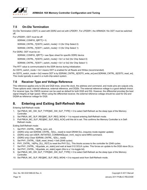
ARMADA 16X Memory Controller Configuration <strong>and</strong> Tuning<br />
7.5 On-Die Termination<br />
On-Die Termination (ODT) is used with DDR2 <strong>and</strong> not with LPDDR1. For LPDDR1, the ARMADA 16x ODT must be switched<br />
off.<br />
For LPDDR1, ODT must be off:<br />
SDRAM_CONFIG_0[RTT] = 0,<br />
SDRAM_CNTRL_7[ODT0_switch_mode] = 0 (for Chip Select 0)<br />
SDRAM_CNTRL_7[ODT1_switch_mode] = 0 (for Chip Select 1)<br />
For DDR2, ODT must be on:<br />
SDRAM_CONFIG_0[RTT] = see Spec sheet for specific DDR2 device<br />
SDRAM_CNTRL_7[ODT0_switch_mode] = 0x1 or 0x2 (for Chip Select 0)<br />
SDRAM_CNTRL_7[ODT1_switch_mode] = 0x1 or 0x2 (for Chip Select 1)<br />
The RTT value is communicated to the DDR device during initialization.<br />
An ODT0_switch_mode = 0x1 means ODT is enabled for all Reads <strong>and</strong> Writes (recommended).<br />
An ODT0_switch_mode = 0x2 means ODT is by SDRAM_CNTRL_6[ODT0_write_en] <strong>and</strong> SDRAM_CNTRL_6[ODT0_read_en].<br />
This mode typically is used in a multi-chip-select system.<br />
7.6 Receiver Type <strong>and</strong> Voltage Reference<br />
This reference applies only to DQ <strong>and</strong> DQS lines, since the clock, the address <strong>and</strong> comm<strong>and</strong>, <strong>and</strong> mode pins are outputs only.<br />
Three options exist: internal reference, external reference, <strong>and</strong> DQSb. The external reference voltage is a good default choice.<br />
For receiver type, the CMOS receiver can be used as default for both DQS <strong>and</strong> DQ. However, the differential provides the best<br />
signal integrity at high speed. When using the differential receiver, the external reference voltage should be used for DQ <strong>and</strong><br />
DQS# as reference voltage for DQS.<br />
8. Entering <strong>and</strong> Exiting Self-Refresh Mode<br />
Entering Self-Refresh mode:<br />
1. Set PMUA_MC_SW_SLP_TYPE[MC_SW_SLP_TYPE] = 0 to select Self-Refresh as the sleep type of the Memory<br />
Controller.<br />
2. Set PMUA_MC_SLP_REQ[MC_SLP_REQ_MOH] = 1 to request entering Self-Refresh mode.<br />
3. Poll PMUA_MC_SLP_REQ[MC_SLP_REQ_ACK] until this bit is set. This confirms the Memory Controller is in Self-<br />
Refresh mode.<br />
Exiting Self-Refresh mode:<br />
1. Set PHY_CNTRL_14[Phy_sync_en].<br />
2. (DDR2 only) set SDRAM_CNTRL_1[DLL_reset] to reset DRAM DLL (requires mode-register update).<br />
3. (DDR2 only) set USER_INITIATED_COMMAND[user_Imr0_req] to send MRS comm<strong>and</strong>.<br />
4. (DDR2 only) Clear SDRAM_CNTRL_1[DLL_reset].<br />
5. Set PHY_CNTRL_13[dll_reset_timer] = 0x8 (2048 cycles).<br />
6. PHY_CNTRL_14[Phy_DLL_RST] to reset the PHY DLL. This blocks access to the controller for 2048 cycles.<br />
7. Set PHY_CNTRL_14[update_en_static] <strong>and</strong> wait at least 512 DCLK cycles. This forces an update to the DQS slave DLLs.<br />
8. Set PHY_CNTRL_14[update_en_static] again (this is a 1-to-toggle bit).<br />
9. Set PMUA_MC_SW_SLP_TYPE[MC_SW_SLP_TYPE] = 0 to select Self-Refresh as the sleep type of the Memory<br />
Controller.<br />
10. Set PMUA_MC_SLP_REQ[MC_SLP_REQ_MOH] = 0 to request exist from Self-Refresh mode.<br />
Doc. No. MV-S301989-00 Rev. A Copyright © 2011 Marvell<br />
Page 10 January 2011 PUBLIC RELEASE


