3 NTIM and OBM
1. Overview 2. Programming Sequence. 3. NTIM and OBM - Marvell
1. Overview 2. Programming Sequence. 3. NTIM and OBM - Marvell

Create successful ePaper yourself
Turn your PDF publications into a flip-book with our unique Google optimized e-Paper software.
ARMADA 16X Memory Controller Configuration <strong>and</strong> Tuning<br />
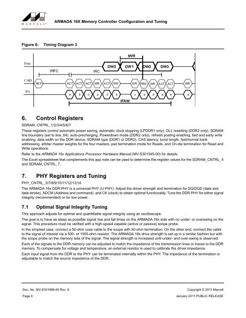
Figure 6: Timing Diagram 3<br />
tWR<br />
Data<br />
tRFC<br />
tRC<br />
DW0<br />
DW1<br />
DW2<br />
DW3<br />
CMD<br />
RE F ACT ACT ACT WR ACT WR WR PRE<br />
WR<br />
ACT<br />
ACT<br />
WR<br />
BA<br />
a<br />
b<br />
c<br />
a<br />
d<br />
b<br />
c<br />
a<br />
d<br />
a<br />
e<br />
e<br />
tFAW<br />
6. Control Registers<br />
SDRAM_CNTRL_1/2/3/4/5/6/7<br />
These registers control automatic power saving, automatic clock stopping (LPDDR1 only), DLL resetting (DDR2 only), SDRAM<br />
line boundary (set to line_64), auto-precharging, Powerdown mode (DDR2 only), refresh posting enabling, fast <strong>and</strong> early write<br />
enabling, data width on the DDR device, SDRAM type (DDR1 or DDR2), CAS latency, burst length, fast/normal bank<br />
addressing, arbiter master weights for the four masters, pad termination mode for Reads, <strong>and</strong> On-die termination for Read <strong>and</strong><br />
Write operations.<br />
Refer to the ARMADA 16x Applications Processor Hardware Manual (MV-S301545-00) for details.<br />
The Excel spreadsheet that complements this app note can be used to determine the register values for the SDRAM_CNTRL_4<br />
<strong>and</strong> SDRAM_CNTRL_7.<br />
7. PHY Registers <strong>and</strong> Tuning<br />
PHY_CNTRL_3/7/8/9/10/11/12/13/14<br />
The ARMADA 16x DDR PHY is a universal PHY (U-PHY). Adjust the driver strength <strong>and</strong> termination for DQ/DQS (data <strong>and</strong><br />
data strobe), ADCM (Address <strong>and</strong> comm<strong>and</strong>), <strong>and</strong> CK (clock) to obtain optimal functionality. Tune the DDR PHY for either signal<br />
integrity (recommended) or for low power.<br />
7.1 Optimal Signal Integrity Tuning<br />
This approach adjusts for optimal <strong>and</strong> quantifiable signal integrity using an oscilloscope.<br />
The goal is to have as steep as possible signal rise <strong>and</strong> fall times on the ARMADA 16x side with no under- or overswing on the<br />
signal. This procedure must be verified with a high-speed capable (active or passive) scope probe.<br />
In the simplest case, connect a 50-ohm coax cable to the scope with 50-ohm termination. On the other end, connect the cable<br />
to the signal of interest via a 500- or 1000-ohm resistor. The ARMADA 16x drive strength is set up in a similar fashion but with<br />
the scope probe on the memory side of the signal. The signal strength is increased until under- <strong>and</strong> over-swing is observed.<br />
Each of the signals to the DDR memory can be adjusted to match the impedance of the transmission lines or traces to the DDR<br />
memory. To compensate for voltage <strong>and</strong> temperature, an external resistor is used to calibrate the driver impedance.<br />
Each input signal from the DDR to the PHY can be terminated internally within the PHY. The impedance of the termination is<br />
adjustable to match the source impedance of the DDR.<br />
Doc. No. MV-S301989-00 Rev. A Copyright © 2011 Marvell<br />
Page 6 January 2011 PUBLIC RELEASE