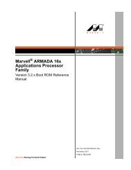
Marvell ARMADA 16x Applications Processor Family
Marvell ARMADA 16x Applications Processor Family
Marvell ARMADA 16x Applications Processor Family

Create successful ePaper yourself
Turn your PDF publications into a flip-book with our unique Google optimized e-Paper software.
Cover<br />
<strong>Marvell</strong> ® <strong>ARMADA</strong> <strong>16x</strong><br />
<strong>Applications</strong> <strong>Processor</strong><br />
<strong>Family</strong><br />
Hardware Manual<br />
Doc. No. MV-S301545-00, Rel. -<br />
November 2010 PUBLIC RELEASE<br />
<strong>Marvell</strong>. Moving Forward Faster
<strong>Marvell</strong> ® <strong>ARMADA</strong> <strong>16x</strong> <strong>Applications</strong> <strong>Processor</strong> <strong>Family</strong> Hardware Manual<br />
Document Conventions<br />
Document Status<br />
Draft<br />
Preliminary<br />
Tapeout<br />
(Advance)<br />
Preliminary<br />
Information<br />
Complete<br />
Information<br />
Milestone Indicator:<br />
Draft = 0.xx<br />
Advance = 1.xx<br />
Preliminary = 2.xx<br />
Complete = 3.xx<br />
Note: Provides related information or information of special importance.<br />
Caution: Indicates potential damage to hardware or software, or loss of data.<br />
Warning: Indicates a risk of personal injury.<br />
For internal use. This document has not passed a complete technical review cycle and ECN signoff<br />
process.<br />
This document contains design specifications for a product in its initial stage of design and development.<br />
A revision of this document or supplementary information may be published at a later date.<br />
<strong>Marvell</strong> may make changes to these specifications at any time without notice.<br />
Contact <strong>Marvell</strong> Field Application Engineers for more information.<br />
This document contains preliminary specifications.<br />
A revision of this document or supplementary information may be published at a later date.<br />
<strong>Marvell</strong> may make changes to these specifications at any time without notice. .<br />
Contact <strong>Marvell</strong> Field Application Engineers for more information.<br />
This document contains specifications for a product in its final qualification stages.<br />
<strong>Marvell</strong> may make changes to these specifications at any time without notice.<br />
Contact <strong>Marvell</strong> Field Application Engineers for more information.<br />
X . Y Z<br />
Work in Progress Indicator<br />
Zero means document is released.<br />
Various Revisions Indicator<br />
Doc Status: Confidential Technical Publication: 3.0<br />
For more information, visit our website at: www.marvell.com<br />
Disclaimer<br />
No part of this document may be reproduced or transmitted in any form or by any means, electronic or mechanical, including photocopying and recording, for any purpose,<br />
without the express written permission of <strong>Marvell</strong>. <strong>Marvell</strong> retains the right to make changes to this document at any time, without notice. <strong>Marvell</strong> makes no warranty of any<br />
kind, expressed or implied, with regard to any information contained in this document, including, but not limited to, the implied warranties of merchantability or fitness for any<br />
particular purpose. Further, <strong>Marvell</strong> does not warrant the accuracy or completeness of the information, text, graphics, or other items contained within this document.<br />
<strong>Marvell</strong> products are not designed for use in life-support equipment or applications that would cause a life-threatening situation if any such products failed. Do not use<br />
<strong>Marvell</strong> products in these types of equipment or applications.<br />
With respect to the products described herein, the user or recipient, in the absence of appropriate U.S. government authorization, agrees:<br />
1) Not to re-export or release any such information consisting of technology, software or source code controlled for national security reasons by the U.S. Export Control<br />
Regulations ("EAR"), to a national of EAR Country Groups D:1 or E:2;<br />
2) Not to export the direct product of such technology or such software, to EAR Country Groups D:1 or E:2, if such technology or software and direct products thereof are<br />
controlled for national security reasons by the EAR; and,<br />
3) In the case of technology controlled for national security reasons under the EAR where the direct product of the technology is a complete plant or component of a plant,<br />
not to export to EAR Country Groups D:1 or E:2 the direct product of the plant or major component thereof, if such direct product is controlled for national security reasons<br />
by the EAR, or is subject to controls under the U.S. Munitions List ("USML").<br />
At all times hereunder, the recipient of any such information agrees that they shall be deemed to have manually signed this document in connection with their receipt of any<br />
such information.<br />
Copyright © 2010. <strong>Marvell</strong> International Ltd. All rights reserved. <strong>Marvell</strong>, the <strong>Marvell</strong> logo, Moving Forward Faster, Alaska, Fastwriter, Datacom Systems on Silicon, Libertas,<br />
Link Street, NetGX, PHYAdvantage, Prestera, Raising The Technology Bar, The Technology Within, Virtual Cable Tester, and Yukon are registered trademarks of <strong>Marvell</strong>.<br />
Ants, AnyVoltage, Discovery, DSP Switcher, Feroceon, GalNet, GalTis, Horizon, <strong>Marvell</strong> Makes It All Possible, RADLAN, UniMAC, and VCT are trademarks of <strong>Marvell</strong>. Intel<br />
XScale® is a trademark or registered trademark of Intel Corporation or its subsidiaries in the United States and other countries. All other trademarks are the property of their<br />
respective owners.<br />
1<br />
2<br />
3<br />
4<br />
5<br />
6<br />
7<br />
8<br />
9<br />
10<br />
11<br />
12<br />
13<br />
14<br />
15<br />
16<br />
17<br />
18<br />
19<br />
20<br />
21<br />
22<br />
23<br />
24<br />
25<br />
26<br />
27<br />
28<br />
29<br />
30<br />
31<br />
32<br />
33<br />
34<br />
35<br />
36<br />
37<br />
38<br />
39<br />
40<br />
41<br />
42<br />
43<br />
44<br />
45<br />
46<br />
47<br />
48<br />
49<br />
50<br />
51<br />
52<br />
53<br />
54<br />
55<br />
56<br />
57<br />
58<br />
59<br />
Doc. No. MV-S301545-00 Rev. - Copyright © 2010 <strong>Marvell</strong><br />
Page 2<br />
November 2010 PUBLIC RELEASE
Table of Contents<br />
Table of Contents<br />
Revision History ..........................................................................................................................11<br />
Public Release, Release - / (November 2010)................................................................................................11<br />
1 Introduction..................................................................................................................................13<br />
1.1 Product Summary ...........................................................................................................................................13<br />
1.2 Document Purpose .........................................................................................................................................16<br />
1.3 Number Representation ..................................................................................................................................17<br />
1.4 Naming Conventions.......................................................................................................................................17<br />
1.5 Applicable Documents ....................................................................................................................................17<br />
2 Product Overview ........................................................................................................................19<br />
3 Pin and Ball Map Views...............................................................................................................21<br />
3.1 <strong>ARMADA</strong> 168 (88AP168) <strong>Applications</strong> <strong>Processor</strong> 15mm x 15mm TFBGA Ball Map .....................................21<br />
3.2 <strong>ARMADA</strong> 166 (88AP166) <strong>Applications</strong> <strong>Processor</strong> 15mm x 15mm TFBGA Ball Map .....................................22<br />
3.3 <strong>ARMADA</strong> 162 (88AP162) <strong>Applications</strong> <strong>Processor</strong> 15mm x 15mm TFBGA Ball Map .....................................23<br />
4 Package Information ...................................................................................................................25<br />
4.1 Introduction .....................................................................................................................................................25<br />
4.2 Package Marking ............................................................................................................................................26<br />
4.3 Packaging Materials........................................................................................................................................26<br />
4.4 <strong>ARMADA</strong> <strong>16x</strong> <strong>Applications</strong> <strong>Processor</strong> <strong>Family</strong> 15mm x 15mm TFBGA Packaging .........................................27<br />
5 Maximum Ratings and Operation Conditions...........................................................................29<br />
5.1 Absolute Maximum Ratings ............................................................................................................................29<br />
5.2 Operating Conditions ......................................................................................................................................30<br />
6 Electrical Specifications .............................................................................................................33<br />
6.1 DC Voltage and Current Characteristics .........................................................................................................33<br />
6.2 Oscillator Electrical Specifications...................................................................................................................37<br />
6.2.1 26.000 MHz Oscillator Specifications ...............................................................................................37<br />
7 AC Electrical Characteristics .....................................................................................................41<br />
7.1 DDR SDRAM Timing Diagrams and Specifications ........................................................................................41<br />
7.1.1 Measurement Conditions..................................................................................................................42<br />
7.1.2 DDR SDRAM Timing Diagrams and Specifications..........................................................................42<br />
7.1.3 DDR SDRAM Skew Timings.............................................................................................................45<br />
7.2 Static Memory Controller Timing Diagrams and Specifications ......................................................................52<br />
7.2.1 Address Cycle...................................................................................................................................52<br />
7.2.2 Read Access Data Phases ...............................................................................................................54<br />
7.2.3 Write Access Data Phases ...............................................................................................................58<br />
Copyright © 2010 <strong>Marvell</strong> Doc. No. MV-S301545-00 Rev. -<br />
November 2010 PUBLIC RELEASE Page 3
<strong>Marvell</strong> ® <strong>ARMADA</strong> <strong>16x</strong> <strong>Applications</strong> <strong>Processor</strong> <strong>Family</strong> Hardware Manual<br />
7.3 NAND Timing Diagrams and Specifications....................................................................................................64<br />
7.3.1 NAND Flash Program Timing ...........................................................................................................64<br />
7.3.2 NAND Flash Erase Timing................................................................................................................64<br />
7.3.3 Small Block NAND Flash Read Timing.............................................................................................65<br />
7.3.4 Large Block NAND Flash Read Timing ............................................................................................65<br />
7.3.5 NAND Flash Status Read Timing .....................................................................................................66<br />
7.3.6 NAND Flash ID Read Timing............................................................................................................66<br />
7.3.7 NAND Flash Reset Timing................................................................................................................67<br />
7.3.7.1 NAND Flash Timing Parameters ........................................................................................67<br />
7.4 SD Host Controller (SDH) Timing Diagrams and Specifications.....................................................................69<br />
7.5 LCD Controller Timing Diagrams and Specifications ......................................................................................70<br />
7.5.1 LCD Smart Panel Timing and Specifications....................................................................................70<br />
7.5.2 LCD Dumb Panel Timing and Specifications....................................................................................73<br />
7.6 Quick Capture Camera Interface (CCIC) Timing Diagrams and Specifications..............................................76<br />
7.6.1 CCIC Parallel Interface Timing Requirements..................................................................................76<br />
7.7 SSP Timing Diagrams and Specifications.......................................................................................................76<br />
7.7.1 SSP Slave Mode Timing...................................................................................................................78<br />
7.8 TWSI Timing Diagrams and Specifications.....................................................................................................79<br />
7.8.1 TWSI Test Circuit..............................................................................................................................81<br />
7.9 AC’97 Timing Diagrams and Specifications ....................................................................................................82<br />
7.10 JTAG Interface Timing Diagrams and Specifications......................................................................................82<br />
7.10.1 JTAG Interface Timing Diagrams .....................................................................................................83<br />
7.10.2 JTAG Interface AC Timing Table......................................................................................................83<br />
7.10.3 JTAG Interface Test Circuit ..............................................................................................................84<br />
7.11 USB 2.0 Timing Diagrams and Specifications.................................................................................................85<br />
7.11.1 USB Interface Driver Waveforms......................................................................................................85<br />
7.11.2 Differential Interface Electrical Characteristics .................................................................................86<br />
7.11.2.1 USB Driver and Receiver Characteristics ..........................................................................86<br />
7.12 PCI Express Specifications .............................................................................................................................88<br />
7.12.1 PCIE Differential TX Output Electrical Characteristics......................................................................88<br />
7.12.2 PCIE Differential RX Input Electrical Characteristics........................................................................89<br />
7.13 Ethernet MAC (MII) Timing Diagrams and Specifications...............................................................................90<br />
7.14 Powerup/Down Sequences.............................................................................................................................92<br />
7.14.1 Power Up Timings ............................................................................................................................92<br />
7.14.1.1 Host Side PMIC USB Signals.............................................................................................92<br />
7.14.2 Powerdown Timings .........................................................................................................................95<br />
8 Design Guidelines and Checklist...............................................................................................97<br />
8.1 DDR Interface General Routing Guidelines ....................................................................................................97<br />
8.1.1 General Rules:..................................................................................................................................97<br />
8.1.1.1 Data and QS Signals..........................................................................................................97<br />
8.1.1.2 Address/Command Signals................................................................................................98<br />
8.1.1.3 Clock Signals......................................................................................................................98<br />
8.1.2 DDR Interface Detailed Routing Guidelines .....................................................................................98<br />
Doc. No. MV-S301545-00 Rev. - Copyright © 2010 <strong>Marvell</strong><br />
Page 4<br />
November 2010 PUBLIC RELEASE
Table of Contents<br />
8.2 EPD Controller Design Guidelines ..................................................................................................................98<br />
8.2.1 Introduction .......................................................................................................................................99<br />
8.2.2 Panel Power Up Sequence...............................................................................................................99<br />
8.2.3 Display Common Power Signal ......................................................................................................100<br />
8.2.3.1 Vcom Setting by DPOT (Digital Potentiometer) ...............................................................100<br />
8.2.4 Source Driver Interface...................................................................................................................101<br />
8.2.5 Gate Driver Interface ......................................................................................................................103<br />
8.2.6 Start Pulse Control..........................................................................................................................104<br />
8.3 Schematic Checklist......................................................................................................................................105<br />
Copyright © 2010 <strong>Marvell</strong> Doc. No. MV-S301545-00 Rev. -<br />
November 2010 PUBLIC RELEASE Page 5
<strong>Marvell</strong> ® <strong>ARMADA</strong> <strong>16x</strong> <strong>Applications</strong> <strong>Processor</strong> <strong>Family</strong> Hardware Manual<br />
Doc. No. MV-S301545-00 Rev. - Copyright © 2010 <strong>Marvell</strong><br />
Page 6<br />
November 2010 PUBLIC RELEASE
List of Figures<br />
List of Figures<br />
Revision History .............................................................................................................................. 11<br />
1 Introduction...................................................................................................................................... 13<br />
2 Product Overview ............................................................................................................................ 19<br />
Figure 1: <strong>ARMADA</strong> <strong>16x</strong> <strong>Applications</strong> <strong>Processor</strong> <strong>Family</strong> Block Diagram ..........................................................20<br />
3 Pin and Ball Map Views................................................................................................................... 21<br />
Figure 2: <strong>ARMADA</strong> 168 (88AP168) <strong>Applications</strong> <strong>Processor</strong> 15mm x 15mmTF-BGA Ball Map - Top View.....22<br />
Figure 3: <strong>ARMADA</strong> 166 (88AP166) <strong>Applications</strong> <strong>Processor</strong> 15mm x 15mmTF-BGA Ball Map - Top View.....23<br />
Figure 4: <strong>ARMADA</strong> 162 (88AP162) <strong>Applications</strong> <strong>Processor</strong> 15mm x 15mmTF-BGA Ball Map - Top View.....24<br />
4 Package Information ....................................................................................................................... 25<br />
Figure 5: Sample Package Marking.................................................................................................................26<br />
Figure 6: <strong>ARMADA</strong> <strong>16x</strong> <strong>Applications</strong> <strong>Processor</strong> <strong>Family</strong> 15mm x 15mm TFBGA Package Information...........27<br />
5 Maximum Ratings and Operation Conditions............................................................................... 29<br />
6 Electrical Specifications ................................................................................................................. 33<br />
Figure 7: Recommended GND Shielding to xtal_in and xtal_out.....................................................................38<br />
7 AC Electrical Characteristics.......................................................................................................... 41<br />
Figure 8: Differential Clock...............................................................................................................................42<br />
Figure 9: LPDDR1 SDRAM Timing Diagrams 1...............................................................................................43<br />
Figure 10: LPDDR1 SDRAM Timing Diagrams 2...............................................................................................43<br />
Figure 11: LPDDR1 SDRAM Timing Diagrams 3...............................................................................................44<br />
Figure 12: LPDDR1 SDRAM Timing Diagrams 4...............................................................................................44<br />
Figure 13: Basic Write Timing Parameters ........................................................................................................45<br />
Figure 14: DQ to DQS Write Skew ....................................................................................................................46<br />
Figure 15: CLK to Address/Command Write Skew............................................................................................46<br />
Figure 16: DQS to CLK Write Skew...................................................................................................................46<br />
Figure 17: DQ to DQS Read Skew ....................................................................................................................47<br />
Figure 18: A/D Address Phase ..........................................................................................................................53<br />
Figure 19: AA/D Address Phase ........................................................................................................................54<br />
Figure 20: Asynchronous Read With RDY Signal..............................................................................................55<br />
Figure 21: Asynchronous Read Without RDY Signal.........................................................................................56<br />
Figure 22: Synchronous Read With RDY Signal ...............................................................................................57<br />
Figure 23: Synchronous Read Without RDY Signal ..........................................................................................58<br />
Figure 24: Asynchronous Write With RDY Signal..............................................................................................59<br />
Figure 25: Asynchronous Write Data Phase Without RDY Signal .....................................................................60<br />
Figure 26: Synchronous Write With RDY Signal................................................................................................61<br />
Figure 27: Synchronous Write Data Phase Without RDY Signal.......................................................................62<br />
Copyright © 2010 <strong>Marvell</strong> Doc. No. MV-S301545-00 Rev. -<br />
November 2010 PUBLIC RELEASE Page 7
<strong>Marvell</strong> ® <strong>ARMADA</strong> <strong>16x</strong> <strong>Applications</strong> <strong>Processor</strong> <strong>Family</strong> Hardware Manual<br />
Figure 28: NAND Flash Program Timing Diagram.............................................................................................64<br />
Figure 29: NAND Flash Erase Timing Diagram .................................................................................................65<br />
Figure 30: NAND Flash Small Block Read Timing Diagram ..............................................................................65<br />
Figure 31: NAND Flash Large Block Read Timing Diagram..............................................................................66<br />
Figure 32: NAND Flash Status Read Timing Diagram.......................................................................................66<br />
Figure 33: NAND Flash ID Read Timing Diagram .............................................................................................67<br />
Figure 34: NAND Flash Reset Timing Diagram .................................................................................................67<br />
Figure 35: MultiMedia Card Timing Diagrams....................................................................................................69<br />
Figure 36: Smart Panel Interface 8-bit 8080-Series Parallel Mode Read Interface Protocol.............................71<br />
Figure 37: Smart Panel Interface 8-bit 8080-Series Parallel Mode Write Interface Protocol .............................71<br />
Figure 38: Smart Panel Interface 8-bit 6800-Series Parallel Mode Read Interface Protocol.............................72<br />
Figure 39: Smart Panel Interface 8-bit 6800-Series Parallel Mode Write Interface Protocol .............................72<br />
Figure 40: SPI Write/Read Protocol...................................................................................................................73<br />
Figure 41: Dumb LCD Panel Horizontal Timing.................................................................................................74<br />
Figure 42: Dumb LCD Panel Vertical Timing .....................................................................................................74<br />
Figure 43: Parallel Timing Diagram ...................................................................................................................76<br />
Figure 44: SSP Master Mode Timing Diagram ..................................................................................................77<br />
Figure 45: SSP Slave Mode Timing Definitions .................................................................................................78<br />
Figure 46: TWSI Output Delay AC Timing Diagram...........................................................................................79<br />
Figure 47: TWSI Output Delay AC Timing Diagram...........................................................................................79<br />
Figure 48: TWSI Test Circuit..............................................................................................................................81<br />
Figure 49: AC’97 CODEC Timing Diagram........................................................................................................82<br />
Figure 50: JTAG Interface Output Delay AC Timing Diagram ...........................................................................83<br />
Figure 51: JTAG Interface Input AC Timing Diagram ........................................................................................83<br />
Figure 52: JTAG Interface Test Circuit ..............................................................................................................84<br />
Figure 53: Low/Full Speed Data Signal Rise and Fall Time ..............................................................................85<br />
Figure 54: High Speed TX Eye Diagram Pattern Template ...............................................................................85<br />
Figure 55: High Speed RX Eye Diagram Pattern Template...............................................................................86<br />
Figure 56: MII Tx Mode Interface Timing Diagrams...........................................................................................90<br />
Figure 57: MII Rx Model Interface Timing Diagrams..........................................................................................91<br />
Figure 58: MII Management Interface Timing Diagrams....................................................................................91<br />
Figure 59: Power-Up Reset Timing....................................................................................................................94<br />
Figure 60: Powerdown Timing ...........................................................................................................................96<br />
8 Design Guidelines and Checklist ................................................................................................... 97<br />
Figure 61: Panel Power Sequence ..................................................................................................................100<br />
Figure 62: DPOT Programming Sequence ......................................................................................................101<br />
Figure 63: Source Driver Connections.............................................................................................................102<br />
Figure 64: Source Driver Timing ......................................................................................................................103<br />
Figure 65: Gate Driver Connections ................................................................................................................104<br />
Figure 66: Gate Driver Output Enable Timing..................................................................................................104<br />
Doc. No. MV-S301545-00 Rev. - Copyright © 2010 <strong>Marvell</strong><br />
Page 8<br />
November 2010 PUBLIC RELEASE
List of Tables<br />
List of Tables<br />
Revision History ...............................................................................................................................11<br />
1 Introduction.......................................................................................................................................13<br />
Table 1: <strong>ARMADA</strong> <strong>16x</strong> <strong>Applications</strong> <strong>Processor</strong> <strong>Family</strong> Feature Breakdown ..................................................14<br />
Table 2: <strong>ARMADA</strong> <strong>16x</strong> <strong>Applications</strong> <strong>Processor</strong> <strong>Family</strong> Hardware Features2.................................................14<br />
Table 3: Supplemental Documentation...........................................................................................................17<br />
2 Product Overview .............................................................................................................................19<br />
3 Pin and Ball Map Views....................................................................................................................21<br />
4 Package Information ........................................................................................................................25<br />
Table 4: Package Materials ............................................................................................................................26<br />
Table 5: TFBGA Package Dimensions ...........................................................................................................28<br />
5 Maximum Ratings and Operation Conditions................................................................................29<br />
Table 6: Absolute Maximum Ratings ..............................................................................................................29<br />
Table 7: Voltage, Temperature, and Frequency Electrical Specifications ......................................................30<br />
6 Electrical Specifications ..................................................................................................................33<br />
Table 8: LPDDR1/LPDDR2 Input, Output and I/O pins AC/DC Operating Conditions ...................................33<br />
Table 9: DDR3 Input, Output, and I/O Pins AC/DC Operating Conditions......................................................34<br />
Table 10: MFP Input, Output, and I/O Pins DC Operating Conditions..............................................................35<br />
Table 11: Typical 26.000 MHz Crystal Requirements.......................................................................................38<br />
Table 12: Typical External 26.000 MHz Oscillator Requirements.....................................................................38<br />
7 AC Electrical Characteristics...........................................................................................................41<br />
Table 13: Standard Input, Output, and I/O-Pin AC Operating Conditions ........................................................42<br />
Table 14: Clock Parameters .............................................................................................................................42<br />
Table 15: DDR Timing Specifications ...............................................................................................................47<br />
Table 16: DDR Timing Specifications for 533 MHz (VDD_M = 1.8V) ...............................................................48<br />
Table 17: DDR Timing Specifications for 400 MHz (VDD_M = 1.8V) ...............................................................49<br />
Table 18: DDR Timing Specifications for 200 MHz (VDD_M = 1.8V) ...............................................................51<br />
Table 19: Static Memory Controller Interface Timing Specifications ................................................................62<br />
Table 20: NAND Flash Interface Program Timing Specifications .....................................................................68<br />
Table 21: MultiMedia Card Timing Specifications.............................................................................................69<br />
Table 22: SD/SDIO Timing Specifications ........................................................................................................70<br />
Table 23: LCD Smart Panel Controller Timing .................................................................................................73<br />
Table 24: LCD Dumb Panel Timing ..................................................................................................................74<br />
Table 25: CCIC Parallel Timing ........................................................................................................................76<br />
Table 26: SSP Master Mode Timing Specifications..........................................................................................77<br />
Table 27: SSP Slave Mode Timing Specifications............................................................................................78<br />
Table 28: TWSI Master AC Timing Table (Standard Mode 100 kHz)...............................................................79<br />
Copyright © 2010 <strong>Marvell</strong> Doc. No. MV-S301545-00 Rev. -<br />
November 2010 PUBLIC RELEASE Page 9
<strong>Marvell</strong> ® <strong>ARMADA</strong> <strong>16x</strong> <strong>Applications</strong> <strong>Processor</strong> <strong>Family</strong> Hardware Manual<br />
Table 29: TWSI Master AC Timing Table (Fast Mode 400 kHz).......................................................................80<br />
Table 30: TWSI Master AC Timing Table (high) speed 3.4 MHz).....................................................................81<br />
Table 31: AC’97 CODEC Timing Specifications ...............................................................................................82<br />
Table 32: JTAG Interface 10 MHz AC Timing1 ................................................................................................83<br />
Table 33: USB Low Speed Driver and Receiver Characteristics1....................................................................86<br />
Table 34: USB Full Speed Driver and Receiver Characteristics1.....................................................................87<br />
Table 35: USB High Speed Driver and Receiver Characteristics1 ...................................................................88<br />
Table 36: PCI Express TX Output Electrical Specifications..............................................................................89<br />
Table 37: PCI Express RX Input Electrical Specifications ................................................................................89<br />
Table 38: MII Tx Mode Interface Timing Specifications....................................................................................90<br />
Table 39: MII Rx Mode Interface Timing Specifications ...................................................................................91<br />
Table 40: MII Management Interface Timing Specifications.............................................................................91<br />
Table 41: Terminology ......................................................................................................................................92<br />
Table 42: Power-Up Timing Specifications.......................................................................................................94<br />
Table 43: Powerdown Timing Specifications ....................................................................................................96<br />
8 Design Guidelines and Checklist ....................................................................................................97<br />
Table 44: Source Driver Signals .....................................................................................................................101<br />
Table 45: Output Gate Driver Signals.............................................................................................................103<br />
Table 46: <strong>ARMADA</strong> <strong>16x</strong> <strong>Applications</strong> <strong>Processor</strong> <strong>Family</strong> Schematic Checklist ...............................................105<br />
Doc. No. MV-S301545-00 Rev. - Copyright © 2010 <strong>Marvell</strong><br />
Page 10<br />
November 2010 PUBLIC RELEASE
Revision History<br />
Public Release, Release - / (November 2010)<br />
Revision History<br />
Public Release, Release - / (November 2010)<br />
• Initial Release<br />
Copyright © 2010 <strong>Marvell</strong> Doc. No. MV-S301545-00 Rev. -<br />
November 2010 PUBLIC RELEASE Page 11
<strong>Marvell</strong> ® <strong>ARMADA</strong> <strong>16x</strong> <strong>Applications</strong> <strong>Processor</strong> <strong>Family</strong> Hardware Manual<br />
Doc. No. MV-S301545-00 Rev. - Copyright © 2010 <strong>Marvell</strong><br />
Page 12<br />
November 2010 PUBLIC RELEASE
Introduction<br />
Product Summary<br />
1 Introduction<br />
Here’s how to correlate the various Public Release versions of <strong>Marvell</strong> ® <strong>ARMADA</strong> <strong>16x</strong><br />
<strong>Applications</strong> <strong>Processor</strong> <strong>Family</strong> documentation:<br />
Note<br />
Rev. - : signifies initial version of any release.<br />
Rev. A: first revision of any release.<br />
This chapter describes:<br />
Rev. B: second revision of any release.<br />
• Section 1.1, Product Summary<br />
• Section 1.2, Document Purpose<br />
• Section 1.3, Number Representation<br />
• Section 1.4, Naming Conventions<br />
• Section 1.5, Applicable Documents<br />
The <strong>Marvell</strong>® <strong>ARMADA</strong> <strong>16x</strong> <strong>Applications</strong> <strong>Processor</strong> <strong>Family</strong> (also referred to as the <strong>ARMADA</strong> <strong>16x</strong><br />
<strong>Applications</strong> <strong>Processor</strong> <strong>Family</strong>) is a high-performance and highly integrated family of devices<br />
optimized for digital picture frames, personal media players, and other personal consumer devices.<br />
Featuring an advanced 1 GHz processor ARM v5TE-compatible core with an integrated 2-D<br />
graphics engine, the <strong>ARMADA</strong> <strong>16x</strong> <strong>Applications</strong> <strong>Processor</strong> <strong>Family</strong> offers performance headroom<br />
and flexibility for today and future applications. The common software base provides a scalable<br />
platform to cover a breadth of product offerings.<br />
Multiple complete turn-key hardware/software reference designs are available for digital picture<br />
frame, personal navigation, and portable media applications for rapid development and quick time to<br />
market. The digital picture frame platform is based on the optimized chipset of the <strong>ARMADA</strong> <strong>16x</strong><br />
<strong>Applications</strong> <strong>Processor</strong> <strong>Family</strong>, <strong>Marvell</strong> Power Management IC, and <strong>Marvell</strong> Wi-Fi component. Ideal<br />
for digital picture frame applications, the <strong>ARMADA</strong> <strong>16x</strong> <strong>Applications</strong> <strong>Processor</strong> <strong>Family</strong>-based<br />
platform delivers fast response time for sophisticated user interfaces, image processing, and<br />
multimedia applications. Software supports multiple A/V standards and photo-editing capabilities for<br />
pan, zoom, and media effects. The <strong>ARMADA</strong> <strong>16x</strong> <strong>Applications</strong> <strong>Processor</strong> <strong>Family</strong> is designed for high<br />
performance and low power, delivering extended battery life for personal consumer devices.<br />
1.1 Product Summary<br />
Rev. B1: first minor revision of Rev. B, usually to correct documentation errors not<br />
attributed to engineering changes.<br />
The <strong>ARMADA</strong> <strong>16x</strong> <strong>Applications</strong> <strong>Processor</strong> <strong>Family</strong> comprises several products. These products<br />
support a variety of options for packaging, speed, on-chip cache and peripheral support. Table 1<br />
shows a breakdown of the <strong>ARMADA</strong> <strong>16x</strong> <strong>Applications</strong> <strong>Processor</strong> <strong>Family</strong> and the options available.<br />
Refer to Table 2 for the basic features of the <strong>ARMADA</strong> <strong>16x</strong> <strong>Applications</strong> <strong>Processor</strong> <strong>Family</strong>.<br />
Copyright © 2010 <strong>Marvell</strong> Doc. No. MV-S301545-00 Rev. -<br />
November 2010 PUBLIC RELEASE Page 13
<strong>Marvell</strong> ® <strong>ARMADA</strong> <strong>16x</strong> <strong>Applications</strong> <strong>Processor</strong> <strong>Family</strong> Hardware Manual<br />
Table 1:<br />
<strong>ARMADA</strong> <strong>16x</strong> <strong>Applications</strong> <strong>Processor</strong> <strong>Family</strong> Feature Breakdown<br />
<strong>ARMADA</strong> 162 <strong>ARMADA</strong> 166 <strong>ARMADA</strong> 166E <strong>ARMADA</strong> 168<br />
Package BGA-320 BGA-320 BGA-320 BGA-320<br />
Max CPU Speed 400 MHz 800 MHz 800 MHz 1.066 GHz<br />
WMMX2 Yes Yes Yes Yes<br />
Memory<br />
(x16 DRAM)<br />
LP-DDR1-200<br />
DDR2-400<br />
DDR3-400<br />
LP-DDR1-200<br />
DDR2-800<br />
DDR3-800<br />
LP-DDR1-200<br />
DDR2-800<br />
DDR3-800<br />
LP-DDR1-200<br />
DDR2-1066<br />
DDR3-1066<br />
L1, L2 Caches 32/32/64 KB 32/32/128 KB 32/32/128 KB 32/32/128 KB<br />
LCD Max Res,<br />
XGA 24bpp WUXGA 24bpp WUXGA 24bpp WUXGA 24bpp<br />
Color<br />
2D and Qdeo<br />
ICR<br />
Yes Yes Yes Yes<br />
USB2.0 HS + PHY* 1 OTG, 1 host 1 OTG, 1 host 1 OTG, 1 host 1 OTG, 1 host<br />
xD Picture Card Yes Yes Yes Yes<br />
CompactFlash+ Yes Yes Yes Yes<br />
FE MAC - Yes Yes Yes<br />
PCIe2.0 x1 Lane - - - Yes<br />
ElectroPhoretic<br />
Display (EPD)<br />
- - Yes -<br />
Table 2: <strong>ARMADA</strong> <strong>16x</strong> <strong>Applications</strong> <strong>Processor</strong> <strong>Family</strong> Hardware Features 2<br />
Feature Group Feature Description<br />
<strong>Marvell</strong>® Sheeva Core<br />
and Internal Memory<br />
MULTIMEDIA<br />
<strong>Marvell</strong> ® Sheeva Embedded CPU<br />
Technology<br />
ARM* v5TE instruction set compliant<br />
L1 Instruction and Data Cache 32 KB I$ + 32 KB D$<br />
L2 Cache<br />
128 KB<br />
Internal Boot ROM<br />
Support boot from 8-bit NAND, 16-bit NAND,<br />
MMC, SD, OneNAND, SLC, MLC NAND,<br />
SSP SPI, and XIP<br />
Multimedia acceleration with WMMX • Decode H.264 up to WVGA and<br />
MPEG-4 up to 720p<br />
Hardware 2D graphics<br />
• Scaling<br />
• Color Space Conversion<br />
• Overlaying<br />
• Rotation<br />
Doc. No. MV-S301545-00 Rev. - Copyright © 2010 <strong>Marvell</strong><br />
Page 14<br />
November 2010 PUBLIC RELEASE
Introduction<br />
Product Summary<br />
Table 2: <strong>ARMADA</strong> <strong>16x</strong> <strong>Applications</strong> <strong>Processor</strong> <strong>Family</strong> Hardware Features 2<br />
Feature Group Feature Description<br />
DMA<br />
EXTERNAL MEMORY<br />
2D Graphics<br />
Bit blt<br />
Qdeo Intelligent Color Remapping • Qdeo ICR enhances color to make<br />
vivid images without hue shifts or<br />
clipping<br />
• Part of the award-winning Qdeo suite of<br />
video processing<br />
CCIR-656 Camera Interface<br />
LCD Controller • Up to WUXGA (1920x1200)<br />
• 16-, 18- or 24 1 -bpp color depth<br />
DMA Controller Interface<br />
DDR Memory Controller • 2 Chip Selects<br />
• 16-bit DDR2/DDR3 at up to 533 MHz<br />
• LP-DDR1<br />
Static Memory Controller • 2 Chip Selects<br />
• AA/D and A/D Muxed Mode support<br />
• Support for VLIO or Companion Chips<br />
NAND Memory Controller • 2 Chip Selects<br />
• SLC and MLC NAND<br />
• x8 and x16 1 small block and large block<br />
Compact Flash Controller • 2 Chip Selects<br />
• Compliant with CompactFlash (CF+)<br />
Spec 4.1<br />
xD Card Controller • 1 Chip Select<br />
• Compliant with xD-Picture Card<br />
Specification Version 1.20<br />
MultiMediaCard/SD/SDIO Card and<br />
MS/MSPRO Controller<br />
• Up to 4 MMC/SD/SDIO Controllers<br />
• 1 Memory Stick Pro Controller w/ support<br />
for 1 Card and support serial interface<br />
and 4-bit parallel interface<br />
Copyright © 2010 <strong>Marvell</strong> Doc. No. MV-S301545-00 Rev. -<br />
November 2010 PUBLIC RELEASE Page 15
<strong>Marvell</strong> ® <strong>ARMADA</strong> <strong>16x</strong> <strong>Applications</strong> <strong>Processor</strong> <strong>Family</strong> Hardware Manual<br />
Table 2: <strong>ARMADA</strong> <strong>16x</strong> <strong>Applications</strong> <strong>Processor</strong> <strong>Family</strong> Hardware Features 2<br />
Feature Group Feature Description<br />
PERIPHERALS USB 2.0 Host Controller 1 High-Speed USB2.0 Host with integrated<br />
transceiver<br />
USB 2.0 OTG Controller<br />
1 High-Speed USB2.0 OTG with integrated<br />
transceiver and boot support<br />
Fast Ethernet Interface • MII interface support 10/100 Ethernet<br />
Operation<br />
• MDC/MDIO interface for external PHY<br />
control<br />
Synchronous Serial Port Controller • Up to 52 MHz with Master and Slave<br />
modes for frame sync and bit clock<br />
• I 2 S support<br />
• Up to 5 general purpose SSPs<br />
Universal Asynchronous Serial Port<br />
Controller<br />
1.2 Document Purpose<br />
• 3 UART Controllers<br />
• Up to 3.6 Mbps data rate<br />
Two Wire Serial Bus Interface (TWSI) 1 • Interfaces to TWSI* peripherals<br />
• Up to 3.4 Mbps with 7-bit addressing<br />
Power Two Wire Serial Bus Interface • Interfaces to TWSI* peripherals<br />
(PWR_TWSI) 1 • Up to 400 kbps with 7-bit addressing<br />
JTAG Controller<br />
JTAG support for debugging and testing<br />
Program Flash<br />
Pulse Width Modulator (PWM) Controller 4 PWM Controllers<br />
HW Timers • Provides three 32-bit General Purpose<br />
Timers<br />
• Provides one 16-bit Watchdog timer<br />
AC ‘97 Interface<br />
Supports the Audio CODEC’97 Component<br />
Specification, Revision 2.3<br />
One-Wire Interface<br />
Serial bus operation to receive/transmit<br />
1-Wire bus data<br />
Keypad Controller • Support for up to 8x8 Matrix Keys<br />
• Support for up to 8 Direct Keys<br />
General Purpose Input/Output (GPIO)<br />
Controller<br />
1. Two-Wire Serial Interface (formerly referred to as I 2 C)<br />
2. Not all features may be present in all SKUs - contact your <strong>Marvell</strong> sales rep.<br />
Up to 123 Multi-Function Pins with alternate<br />
GPIO functionality<br />
This document constitutes the hardware specifications for the <strong>ARMADA</strong> <strong>16x</strong> <strong>Applications</strong> <strong>Processor</strong><br />
<strong>Family</strong>, including electrical, mechanical, and thermal information, functional overview, mechanical<br />
data, package signal locations, targeted electrical specifications, functional bus waveforms, and<br />
board design considerations. For software specifications including register programming<br />
information, refer to the <strong>Marvell</strong> ® <strong>ARMADA</strong> <strong>16x</strong> Application <strong>Processor</strong> <strong>Family</strong> Software Manual<br />
(MV-S301544-00).<br />
SPECIAL NOTE: Not all of the devices listed in this hardware manual have external hardware<br />
connections. Refer to the software manual (MV-S301544-00) for more information.<br />
Doc. No. MV-S301545-00 Rev. - Copyright © 2010 <strong>Marvell</strong><br />
Page 16<br />
November 2010 PUBLIC RELEASE
Introduction<br />
Number Representation<br />
1.3 Number Representation<br />
All numbers in this document are decimal (base 10) unless designated otherwise. Hexadecimal<br />
numbers have a prefix of 0x, and binary numbers have a prefix of 0b. For example, 107 is<br />
represented as 0x6B in hexadecimal and 0b110_1011 in binary.<br />
1.4 Naming Conventions<br />
All signal and register-bit names appear in uppercase. Active low items are prefixed with a<br />
lowercase “n”.<br />
Pins within a signal name are enclosed in angle brackets:<br />
EXTERNAL_ADDRESS<br />
nCS<br />
Bits within a register bit field are enclosed in square brackets:<br />
REGISTER_BITFIELD[3:0]<br />
REGISTER_BIT[0]<br />
Single-bit items have either of two states:<br />
• Clear — the item contains the value 0b0<br />
• Set — the item contains the value 0b1<br />
1.5 Applicable Documents<br />
Table 3 lists supplemental information sources for the <strong>ARMADA</strong> <strong>16x</strong> <strong>Applications</strong> <strong>Processor</strong> <strong>Family</strong>.<br />
Contact a <strong>Marvell</strong> representative for the latest document revisions and ordering instructions.<br />
Table 3:<br />
Supplemental <strong>ARMADA</strong> <strong>16x</strong> <strong>Applications</strong> <strong>Processor</strong> <strong>Family</strong><br />
Documentation, Releases, and Availability<br />
Document Title<br />
<strong>ARMADA</strong> <strong>16x</strong> <strong>Applications</strong> <strong>Processor</strong> <strong>Family</strong> Hardware Manual (MV-S301545-00)<br />
Public Release Available<br />
<strong>ARMADA</strong> <strong>16x</strong> <strong>Applications</strong> <strong>Processor</strong> <strong>Family</strong> Software Manual (MV-S301544-00)<br />
Public Release Available<br />
<strong>ARMADA</strong><strong>16x</strong> <strong>Applications</strong> <strong>Processor</strong> <strong>Family</strong> Alternate Function Spreadsheet<br />
<strong>ARMADA</strong> <strong>16x</strong> <strong>Applications</strong> <strong>Processor</strong> <strong>Family</strong> Boot ROM Reference Manual<br />
Public Release Available<br />
<strong>ARMADA</strong> <strong>16x</strong> <strong>Applications</strong> <strong>Processor</strong> <strong>Family</strong> PMIC Application Note<br />
USB 2.0 PHY Calibration/ Compliance Guidelines for <strong>ARMADA</strong> <strong>16x</strong> <strong>Applications</strong><br />
<strong>Processor</strong> <strong>Family</strong> (MV-S301722-00)<br />
<strong>ARMADA</strong> <strong>16x</strong> <strong>Applications</strong> <strong>Processor</strong> <strong>Family</strong> JTAG Application Note<br />
(MV-S301720-00)<br />
<strong>ARMADA</strong> <strong>16x</strong> <strong>Applications</strong> <strong>Processor</strong> <strong>Family</strong> Board Design and Layout Guidelines<br />
(MV-S301721-00)<br />
<strong>ARMADA</strong> <strong>16x</strong> <strong>Applications</strong> <strong>Processor</strong> <strong>Family</strong> Temperature Sensor App Note<br />
(MV-S301707-00)<br />
Available<br />
Now<br />
Now<br />
Now<br />
Now<br />
Now<br />
Now<br />
Now<br />
Now<br />
Now<br />
Copyright © 2010 <strong>Marvell</strong> Doc. No. MV-S301545-00 Rev. -<br />
November 2010 PUBLIC RELEASE Page 17
<strong>Marvell</strong> ® <strong>ARMADA</strong> <strong>16x</strong> <strong>Applications</strong> <strong>Processor</strong> <strong>Family</strong> Hardware Manual<br />
Table 3:<br />
Supplemental <strong>ARMADA</strong> <strong>16x</strong> <strong>Applications</strong> <strong>Processor</strong> <strong>Family</strong><br />
Documentation, Releases, and Availability (Continued)<br />
Document Title<br />
<strong>ARMADA</strong><strong>16x</strong> <strong>Applications</strong> <strong>Processor</strong> <strong>Family</strong> Spec Update(s)<br />
Check the <strong>Marvell</strong> website for the latest versions of available documents<br />
Available<br />
Spec Updates<br />
are released<br />
periodically<br />
Note<br />
Refer to the <strong>Marvell</strong> ® <strong>ARMADA</strong> <strong>16x</strong> <strong>Applications</strong> <strong>Processor</strong> <strong>Family</strong> Specification<br />
Update (MV-S501140-00) for corrections and updates to content between<br />
documentation releases. The specification update is revised on a periodic basis.<br />
Doc. No. MV-S301545-00 Rev. - Copyright © 2010 <strong>Marvell</strong><br />
Page 18<br />
November 2010 PUBLIC RELEASE
Product Overview<br />
2 Product Overview<br />
The <strong>ARMADA</strong> <strong>16x</strong> <strong>Applications</strong> <strong>Processor</strong> <strong>Family</strong> application is an integrated system-on-a-chip<br />
microprocessor targets mid- to high-end picture frame, personal navigation devices, and smart-monitor<br />
applications, among others. It incorporates the <strong>Marvell</strong> ® Sheeva Embedded CPU<br />
Technology microarchitecture with sophisticated power management to provide optimum MIPS/mW<br />
performance across its wide range of operating frequencies. The <strong>ARMADA</strong> <strong>16x</strong> <strong>Applications</strong> <strong>Processor</strong><br />
<strong>Family</strong> complies with the ARM* Architecture V5TE instruction set (excluding floating point<br />
instructions) and follows the ARM* programmers model. The <strong>ARMADA</strong> <strong>16x</strong> <strong>Applications</strong> <strong>Processor</strong><br />
<strong>Family</strong> multimedia coprocessor provides enhanced Intel ® WMMX 2 instructions to accelerate audio<br />
and video processing. The <strong>ARMADA</strong> <strong>16x</strong> <strong>Applications</strong> <strong>Processor</strong> <strong>Family</strong> is available in a discrete<br />
package configuration.<br />
The <strong>ARMADA</strong> <strong>16x</strong> <strong>Applications</strong> <strong>Processor</strong> <strong>Family</strong> memory architecture provides greater flexibility<br />
and higher performance than that of previous products. The <strong>ARMADA</strong> <strong>16x</strong> <strong>Applications</strong> <strong>Processor</strong><br />
<strong>Family</strong> provides the configuration support for two dedicated memory interfaces to support<br />
high-speed DDR SDRAM, VLIO devices, and NAND Flash devices. This flexibility enables high performance<br />
“store and download” as well as “execute-in-place” system architectures. The <strong>ARMADA</strong><br />
<strong>16x</strong> <strong>Applications</strong> <strong>Processor</strong> <strong>Family</strong> memory architecture features a memory switch that allows multiple<br />
simultaneous memory transactions between different sources and targets. For example, the<br />
<strong>ARMADA</strong> <strong>16x</strong> <strong>Applications</strong> <strong>Processor</strong> <strong>Family</strong> architecture allows memory traffic between the core<br />
and DDR SDRAM to move in parallel with DMA-generated traffic between the camera interface and<br />
the LCD Controller.<br />
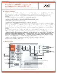
Figure 1 illustrates the <strong>ARMADA</strong> <strong>16x</strong> <strong>Applications</strong> <strong>Processor</strong> <strong>Family</strong>. The diagram shows a<br />
multi-port memory switch and system bus architecture with the core attached, along with an LCD<br />
Controller and hardware accelerators for graphics and color remapping. The key features of all of<br />
the sub-blocks are described in this section, with more detail provided in the respective chapters.<br />
Copyright © 2010 <strong>Marvell</strong> Doc. No. MV-S301545-00 Rev. -<br />
November 2010 PUBLIC RELEASE Page 19
<strong>Marvell</strong> ® <strong>ARMADA</strong> <strong>16x</strong> <strong>Applications</strong> <strong>Processor</strong> <strong>Family</strong> Hardware Manual<br />
Figure 1:<br />
<strong>ARMADA</strong> <strong>16x</strong> <strong>Applications</strong> <strong>Processor</strong> <strong>Family</strong> Block Diagram<br />
Main PMU<br />
Temp<br />
Sensor<br />
Application<br />
Subsystem<br />
PMU<br />
UART 1<br />
UART 2<br />
UART 3<br />
AC97<br />
RTC Timer<br />
Keypad<br />
Controller<br />
TWSI1<br />
PWR_TWSI<br />
OneWire<br />
3x Timers<br />
WDT<br />
General and<br />
Configuration<br />
Registers<br />
APB<br />
Bus<br />
J<br />
T<br />
A<br />
G<br />
Boot<br />
ROM<br />
SQU<br />
AXI<br />
Decoder<br />
L2 $<br />
DMA<br />
XD<br />
Addr Decoder<br />
BIU<br />
<strong>Marvell</strong><br />
Sheeva<br />
Core<br />
L1$<br />
AXI Fabric<br />
SD1 SD2<br />
SDH1<br />
SMC<br />
mcb1<br />
NFC<br />
DDR<br />
Controller<br />
mcb2<br />
SD3 SD4<br />
SDH2<br />
ICU<br />
mcb3<br />
CI<br />
AXI 1<br />
SSP1<br />
APB2 Bus<br />
SSP2 SSP3 SSP4 SSP5<br />
Bridge/<br />
DMA<br />
APB2AXI<br />
AXI-AHB<br />
Bridge<br />
USB 2.0<br />
OTG<br />
CF<br />
AHB<br />
USB 2.0<br />
Host<br />
MS Pro<br />
FE<br />
GC300<br />
CMU<br />
AXI 2<br />
LCD<br />
PCIE<br />
EPD<br />
Doc. No. MV-S301545-00 Rev. - Copyright © 2010 <strong>Marvell</strong><br />
Page 20<br />
November 2010 PUBLIC RELEASE
Pin and Ball Map Views<br />
<strong>ARMADA</strong> 168 (88AP168) <strong>Applications</strong> <strong>Processor</strong> 15mm x 15mm TFBGA Ball Map<br />
3 Pin and Ball Map Views<br />
In the following pin and ball map figures, the lowercase letter “n”, which normally indicates negation,<br />
appears as uppercase “N”. “RFU” means “Reserved For Future Use”. NC means “No Connect”. Do<br />
not connect these pins.<br />
• Section 3.1, <strong>ARMADA</strong> 168 (88AP168) <strong>Applications</strong> <strong>Processor</strong> 15mm x 15mm TFBGA Ball Map<br />
• Section 3.2, <strong>ARMADA</strong> 166 (88AP166) <strong>Applications</strong> <strong>Processor</strong> 15mm x 15mm TFBGA Ball Map<br />
• Section 3.3, <strong>ARMADA</strong> 162 (88AP162) <strong>Applications</strong> <strong>Processor</strong> 15mm x 15mm TFBGA Ball Map<br />
3.1 <strong>ARMADA</strong> 168 (88AP168) <strong>Applications</strong> <strong>Processor</strong><br />
15mm x 15mm TFBGA Ball Map<br />
Figure 2 shows the ball map for the 320-ball 15mm x 15mm TFBGA <strong>ARMADA</strong> 168 (88AP168)<br />
<strong>Applications</strong> <strong>Processor</strong> package.<br />
Copyright © 2010 <strong>Marvell</strong> Doc. No. MV-S301545-00 Rev. -<br />
November 2010 PUBLIC RELEASE Page 21
<strong>Marvell</strong> ® <strong>ARMADA</strong> 100 <strong>Applications</strong> <strong>Processor</strong> <strong>Family</strong> Hardware Manual<br />
Figure 2:<br />
<strong>ARMADA</strong> 168 (88AP168) <strong>Applications</strong> <strong>Processor</strong> 15mm x 15mmTF-BGA Ball Map - Top<br />
View<br />
1 2 3 4 5 6 7 8 9 10 11 12 13 14 15 16 17 18<br />
A MFP_92 MFP_88 MFP_86 MFP_84 MFP_80 MFP_76 MFP_72 MFP_68 MFP_64 MFP_63 MFP_59 MFP_35 MFP_31 MFP_29 MFP_22 MFP_19 MFP_17 MFP_16<br />
B MFP_93 MFP_90 MFP_87 MFP_85 MFP_81 MFP_77 MFP_73 MFP_69 MFP_65 MFP_62 MFP_58 MFP_33 MFP_30 MFP_28 MFP_21 MFP_18 MFP_15 MFP_14<br />
A<br />
B<br />
C MFP_97 MFP_95 MFP_91<br />
VD D_<br />
IO2<br />
MFP_82<br />
VSS<br />
VDD_<br />
IO2<br />
MFP_70<br />
VDD_<br />
IO2<br />
VSS MFP_57 MFP_34 MFP_27 MFP_24 MFP_20 VSS MFP_13 MFP_12 C<br />
D MFP_10<br />
1<br />
MFP_98 MFP_94 MFP_89 MFP_83 MFP_78 MFP_74 MFP_71 MFP_66 MFP_61 MFP_56 MFP_32 MFP_25 MFP_23 MFP_11 MFP_10 MFP_9 MFP_8 D<br />
E MFP_10<br />
4<br />
MFP_10<br />
2<br />
MFP_99 MFP_96 VDD_IO<br />
4<br />
MFP_79 MFP_75<br />
VDD_<br />
CORE<br />
MFP_67 MFP_60<br />
VDD_<br />
CORE<br />
VDD_IO<br />
MFP_36 MFP_26<br />
0<br />
MFP_7 MFP_6 MFP_5 MFP_4 E<br />
F MFP_10<br />
6<br />
MFP_10 MFP_10 MFP_10<br />
5 3 0<br />
VDD_IO<br />
4<br />
VSS VSS VSS VSS VSS VSS<br />
VDD_IO<br />
0<br />
MFP_3 MFP_2 MFP_1 MFP_0 F<br />
G MFP_11<br />
0<br />
MFP_10 MFP_10 MFP_10<br />
9 8 7<br />
VDD_<br />
CORE<br />
VSS VSS VSS VSS VSS VSS VSS VSS<br />
VDD_<br />
CORE<br />
MFP_55 MFP_54 MFP_53 MFP_52 G<br />
H MFP_11<br />
4<br />
MFP_11 MFP_11 MFP_11 VDD_<br />
3 2 1 CORE<br />
VSS VSS VSS VSS VSS VSS VSS VSS<br />
VDD_<br />
CORE<br />
MFP_51 MFP_50 MFP_49 MFP_48 H<br />
J MFP_11<br />
8<br />
MFP_11 MFP_11 MFP_11 VDD_IO<br />
7 6 5 3<br />
VSS VSS VSS VSS VSS VSS VSS VSS<br />
VDD_IO<br />
MFP_44 MFP_45 MFP_46 MFP_47<br />
1<br />
J<br />
K MFP_11<br />
9<br />
MFP_12 MFP_12 MFP_12<br />
0 1 2<br />
VDD_IO<br />
3<br />
VSS VSS VSS VSS VSS VSS VSS VSS<br />
VDD_IO<br />
MFP_40 MFP_41 MFP_42 MFP_43<br />
1<br />
K<br />
L RESET_<br />
IN_N<br />
PWR_S<br />
CL<br />
PWR_S<br />
PRI_TDI<br />
VDD_<br />
DA<br />
CORE<br />
VSS VSS VSS VSS VSS VSS VSS VSS<br />
VDD_<br />
CORE<br />
MFP_37 MFP_38 USBID VSS L<br />
M PRI_TM<br />
S<br />
PRI_TC<br />
K<br />
PRI_TD<br />
O<br />
PRI_TR<br />
ST_N<br />
VDD_C<br />
ORE<br />
VSS VSS VSS VSS VSS VSS VSS VSS<br />
VDD_<br />
CORE<br />
MFP_39<br />
AVDD_<br />
UHC<br />
USBH_<br />
P<br />
USBH_<br />
N<br />
M<br />
N VREF JTAG_S<br />
EL<br />
EXT_WA CALPA<br />
KEUP D<br />
SEC_C<br />
S_EN<br />
VSS VSS SDCKE1 nSDCS1 VSS VSS VSS<br />
AVDD_<br />
OTG<br />
VSS<br />
USBOT<br />
G_P<br />
USBOT<br />
G_N<br />
N<br />
P DQM0 MDQ0 MDQ1 MDQ2 VSS MDQ12 VSS<br />
VDD_<br />
CORE<br />
VDD_M SDBA2<br />
VDD_<br />
CORE<br />
VSS MA13 VSS VSS<br />
AVDD_<br />
OSC<br />
USBVB<br />
US<br />
AVDD5_<br />
USB<br />
P<br />
R DQS0_<br />
N<br />
VDD_M MDQ3 VDD_M MDQ10 MDQ13 SDCKE<br />
0<br />
nSDCS<br />
0<br />
SDBA1 MA0 MA3 MA9 MA12 MA14<br />
RFU_<br />
R15<br />
RT_SEN A_ISET PXTAL_<br />
IN<br />
R<br />
T DQS0 VSS MDQ4 VSS MDQ11 MDQ14 VDD_M VSS SDBA0 VDD_M VSS MA8 VDD_M VSS<br />
AVDDT_<br />
PCIE<br />
VSS<br />
VDD_<br />
CORE<br />
PXTAL_<br />
OUT<br />
T<br />
U MDQ5 MDQ6 VDD_M MDQ9 VDD_M VSS MDQ15 ODT nSDWE MA1 MA4 MA7 MA11 ODT1<br />
PCIETX<br />
P<br />
AVDD_<br />
PCIE<br />
PCIERX PCIECL<br />
P KKP<br />
U<br />
SDCLK SDCLK nSDRA nSDCA<br />
nDDR_ PCIETX<br />
PCIERX PCIECL<br />
V MDQ7 MDM1 MDQ8 DQS1_N DQS1<br />
MA2 MA5 MA6 MA10<br />
VSS<br />
0 0_N S S<br />
RESET N<br />
N KKN<br />
1 2 3 4 5 6 7 8 9 10 11 12 13 14 15 16 17 18<br />
V<br />
3.2 <strong>ARMADA</strong> 166 (88AP166) <strong>Applications</strong> <strong>Processor</strong><br />
15mm x 15mm TFBGA Ball Map<br />
Figure 3 shows the ball map for the 320-ball 15mm x 15mm TFBGA <strong>ARMADA</strong> 166 (88AP166)<br />
<strong>Applications</strong> <strong>Processor</strong> package.<br />
Doc. No. MV-S301545-00 Rev. - Copyright © 2010 <strong>Marvell</strong><br />
Page 22<br />
November 2010 PUBLIC RELEASE
Pin and Ball Map Views<br />
<strong>ARMADA</strong> 162 (88AP162) <strong>Applications</strong> <strong>Processor</strong> 15mm x 15mm TFBGA Ball Map<br />
Figure 3:<br />
<strong>ARMADA</strong> 166 (88AP166) <strong>Applications</strong> <strong>Processor</strong> 15mm x 15mmTF-BGA Ball Map - Top<br />
View<br />
A MFP_92 MFP_88 MFP_86 MFP_84 MFP_80 MFP_76 MFP_72 MFP_68 MFP_64 MFP_63 MFP_59 MFP_35 MFP_31 MFP_29 MFP_22 MFP_19 MFP_17 MFP_16<br />
B MFP_93 MFP_90 MFP_87 MFP_85 MFP_81 MFP_77 MFP_73 MFP_69 MFP_65 MFP_62 MFP_58 MFP_33 MFP_30 MFP_28 MFP_21 MFP_18 MFP_15 MFP_14<br />
A<br />
B<br />
C MFP_97 MFP_95 MFP_91<br />
VD D_<br />
IO2<br />
MFP_82<br />
VSS<br />
VDD_<br />
IO2<br />
MFP_70<br />
VDD_<br />
IO2<br />
VSS MFP_57 MFP_34 MFP_27 MFP_24 MFP_20 VSS MFP_13 MFP_12 C<br />
D MFP_10<br />
1<br />
MFP_98 MFP_94 MFP_89 MFP_83 MFP_78 MFP_74 MFP_71 MFP_66 MFP_61 MFP_56 MFP_32 MFP_25 MFP_23 MFP_11 MFP_10 MFP_9 MFP_8 D<br />
E MFP_10<br />
4<br />
MFP_10<br />
2<br />
MFP_99 MFP_96 VDD_IO<br />
4<br />
MFP_79 MFP_75<br />
VDD_<br />
CORE<br />
MFP_67 MFP_60<br />
VDD_<br />
CORE<br />
VDD_IO<br />
MFP_36 MFP_26<br />
0<br />
MFP_7 MFP_6 MFP_5 MFP_4 E<br />
F MFP_10<br />
6<br />
MFP_10 MFP_10 MFP_10<br />
5 3 0<br />
VDD_IO<br />
4<br />
VSS VSS VSS VSS VSS VSS<br />
VDD_IO<br />
0<br />
MFP_3 MFP_2 MFP_1 MFP_0 F<br />
G MFP_11<br />
0<br />
MFP_10 MFP_10 MFP_10<br />
9 8 7<br />
VDD_<br />
CORE<br />
VSS VSS VSS VSS VSS VSS VSS VSS<br />
VDD_<br />
CORE<br />
MFP_55 MFP_54 MFP_53 MFP_52 G<br />
H MFP_11<br />
4<br />
MFP_11 MFP_11 MFP_11 VDD_<br />
3 2 1 CORE<br />
VSS VSS VSS VSS VSS VSS VSS VSS<br />
VDD_<br />
CORE<br />
MFP_51 MFP_50 MFP_49 MFP_48 H<br />
J MFP_11<br />
8<br />
MFP_11 MFP_11 MFP_11 VDD_IO<br />
7 6 5 3<br />
VSS VSS VSS VSS VSS VSS VSS VSS<br />
VDD_IO<br />
MFP_44 MFP_45 MFP_46 MFP_47<br />
1<br />
J<br />
K MFP_11<br />
9<br />
MFP_12 MFP_12 MFP_12<br />
0 1 2<br />
VDD_IO<br />
3<br />
VSS VSS VSS VSS VSS VSS VSS VSS<br />
VDD_IO<br />
MFP_40 MFP_41 MFP_42 MFP_43<br />
1<br />
K<br />
L RESET_<br />
IN_N<br />
PWR_S<br />
CL<br />
PWR_S<br />
PRI_TDI<br />
VDD_<br />
DA<br />
CORE<br />
VSS VSS VSS VSS VSS VSS VSS VSS<br />
VDD_<br />
CORE<br />
MFP_37 MFP_38 USBID VSS L<br />
M PRI_TM<br />
S<br />
PRI_TC<br />
K<br />
PRI_TD<br />
O<br />
PRI_TR<br />
ST_N<br />
VDD_<br />
CORE<br />
VSS VSS VSS VSS VSS VSS VSS VSS<br />
VDD_<br />
CORE<br />
MFP_39<br />
AVDD_<br />
UHC<br />
USBH_<br />
P<br />
USBH_<br />
N<br />
M<br />
N VREF JTAG_S<br />
EL<br />
EXT_WA CALPA<br />
KEUP D<br />
SEC_C<br />
S_EN<br />
VSS VSS SDCKE1 nSDCS1 VSS VSS VSS<br />
AVDD_<br />
OTG<br />
VS S<br />
USBOT<br />
G_P<br />
USBOT<br />
G_N<br />
N<br />
P DQM0 MDQ0 MDQ1 MDQ2 VSS MDQ12 VSS<br />
VDD_<br />
CORE<br />
VDD_M SDBA2<br />
VDD_<br />
CORE<br />
VSS MA13 VSS VSS<br />
AVDD_<br />
OSC<br />
USBVB<br />
US<br />
AVDD5_<br />
USB<br />
P<br />
R DQS0_<br />
N<br />
VDD_M MDQ3 VDD_M MDQ10 MDQ13 SDCKE<br />
0<br />
nSDCS<br />
0<br />
SDBA1 MA0 MA3 MA9 MA12 MA14 VSS RT_SEN A_ISET PXTAL_<br />
IN<br />
R<br />
T DQS0 VSS MDQ4 VSS MDQ11 MDQ14 VDD_M VSS SDBA0 VDD_M VSS MA8 VDD_M VSS VSS VSS<br />
VDD_<br />
CORE<br />
PXTAL_<br />
OUT<br />
T<br />
U MDQ5 MDQ6 VDD_M MDQ9 VDD_M VSS MDQ15 ODT nSDWE MA1 MA4 MA7 MA11 ODT1 VSS VSS VSS VSS U<br />
SDCLK SDCLK nSDRA nSDCA<br />
nDDR_<br />
V MDQ7 MDM1 MDQ8 DQS1_N DQS1<br />
MA2 MA5 MA6 MA10<br />
VS S VS S VS S VS S V<br />
0 0_N S S<br />
RESET<br />
1 2 3 4 5 6 7 8 9 10 11 12 13 14 15 16 17 18<br />
3.3 <strong>ARMADA</strong> 162 (88AP162) <strong>Applications</strong> <strong>Processor</strong><br />
15mm x 15mm TFBGA Ball Map<br />
Figure 4 shows the ball map for the 320-ball 15mm x 15mm TFBGA <strong>ARMADA</strong> 162 (88AP162)<br />
<strong>Applications</strong> <strong>Processor</strong> package.<br />
Copyright © 2010 <strong>Marvell</strong> Doc. No. MV-S301545-00 Rev. -<br />
November 2010 PUBLIC RELEASE Page 23
<strong>Marvell</strong> ® <strong>ARMADA</strong> 100 <strong>Applications</strong> <strong>Processor</strong> <strong>Family</strong> Hardware Manual<br />
Figure 4:<br />
<strong>ARMADA</strong> 162 (88AP162) <strong>Applications</strong> <strong>Processor</strong> 15mm x 15mmTF-BGA Ball Map - Top<br />
View<br />
1 2 3 4 5 6 7 8 9 10 11 12 13 14 15 16 17 18<br />
A MFP_92 MFP_88 MFP_86 MFP_84 MFP_80 MFP_76 MFP_72 MFP_68 MFP_64 MFP_63 MFP_59 MFP_35 MFP_31 MFP_29 MFP_22 MFP_19 MFP_17 MFP_16<br />
B MFP_93 MFP_90 MFP_87 MFP_85 MFP_81 MFP_77 MFP_73 MFP_69 MFP_65 MFP_62 MFP_58 MFP_33 MFP_30 MFP_28 MFP_21 MFP_18 MFP_15 MFP_14<br />
A<br />
B<br />
C MFP_97 MFP_95 MFP_91<br />
VD D_<br />
IO2<br />
MFP_82<br />
VSS<br />
VDD_<br />
IO2<br />
MFP_70<br />
VDD_<br />
IO2<br />
VSS MFP_57 MFP_34 MFP_27 MFP_24 MFP_20 VSS MFP_13 MFP_12 C<br />
D MFP_10<br />
1<br />
MFP_98 MFP_94 MFP_89 MFP_83 MFP_78 MFP_74 MFP_71 MFP_66 MFP_61 MFP_56 MFP_32 MFP_25 MFP_23 MFP_11 MFP_10 MFP_9 MFP_8 D<br />
E MFP_10<br />
4<br />
MFP_10<br />
2<br />
MFP_99 MFP_96 VDD_IO<br />
4<br />
MFP_79 MFP_75<br />
VDD_<br />
CORE<br />
MFP_67 MFP_60<br />
VDD_<br />
CORE<br />
VDD_IO<br />
MFP_36 MFP_26<br />
0<br />
MFP_7 MFP_6 MFP_5 MFP_4 E<br />
F MFP_10<br />
6<br />
MFP_10 MFP_10 MFP_10<br />
5 3 0<br />
VDD_IO<br />
4<br />
VSS VSS VSS VSS VSS VSS<br />
VDD_IO<br />
0<br />
MFP_3 MFP_2 MFP_1 MFP_0 F<br />
G MFP_11<br />
0<br />
MFP_10 MFP_10 MFP_10<br />
9 8 7<br />
VDD_<br />
CORE<br />
VSS VSS VSS VSS VSS VSS VSS VSS<br />
VDD_<br />
CORE<br />
MFP_55 MFP_54 MFP_53 MFP_52 G<br />
H MFP_11<br />
4<br />
MFP_11 MFP_11 MFP_11 VDD_<br />
3 2 1 CORE<br />
VSS VSS VSS VSS VSS VSS VSS VSS<br />
VDD_<br />
CORE<br />
MFP_51 MFP_50 MFP_49 MFP_48 H<br />
J MFP_11<br />
8<br />
MFP_11 MFP_11 MFP_11 VDD_IO<br />
7 6 5 3<br />
VSS VSS VSS VSS VSS VSS VSS VSS<br />
VDD_IO<br />
MFP_44 MFP_45 MFP_46 MFP_47<br />
1<br />
J<br />
K MFP_11<br />
9<br />
MFP_12 MFP_12 MFP_12<br />
0 1 2<br />
VDD_IO<br />
3<br />
VSS VSS VSS VSS VSS VSS VSS VSS<br />
VDD_IO<br />
MFP_40 MFP_41 MFP_42 MFP_43<br />
1<br />
K<br />
L RESET_<br />
IN_N<br />
PWR_S<br />
CL<br />
PWR_S<br />
PRI_TDI<br />
VDD_<br />
DA<br />
CORE<br />
VSS VSS VSS VSS VSS VSS VSS VSS<br />
VDD_<br />
CORE<br />
MFP_37 MFP_38 USBID VSS L<br />
M PRI_TM<br />
S<br />
PRI_TC<br />
K<br />
PRI_TD<br />
O<br />
PRI_TR<br />
ST_N<br />
VDD_C<br />
ORE<br />
VSS VSS VSS VSS VSS VSS VSS VSS<br />
VDD_<br />
CORE<br />
MFP_39<br />
AVDD_<br />
UHC<br />
USBH_<br />
P<br />
USBH_<br />
N<br />
M<br />
N VREF JTAG_S<br />
EL<br />
EXT_WA CALPA<br />
KEUP D<br />
SEC_C<br />
S_EN<br />
VSS VSS SDCKE1 nSDCS1 VSS VSS VSS<br />
AVDD_<br />
OTG<br />
VS S<br />
USBOT<br />
G_P<br />
USBOT<br />
G_N<br />
N<br />
P DQM0 MDQ0 MDQ1 MDQ2 VSS MDQ12 VSS<br />
VDD_<br />
CORE<br />
VDD_M SDBA2<br />
VDD_<br />
CORE<br />
VSS MA13 VSS VSS<br />
AVDD_<br />
OSC<br />
USBVB<br />
US<br />
AVDD5_<br />
USB<br />
P<br />
R DQS0_<br />
N<br />
VDD_M MDQ3 VDD_M MDQ10 MDQ13 SDCKE<br />
0<br />
nSDCS<br />
0<br />
SDBA1 MA0 MA3 MA9 MA12 MA14 VSS RT_SEN A_ISET PXTAL_<br />
IN<br />
R<br />
T DQS0 VSS MDQ4 VSS MDQ11 MDQ14 VDD_M VSS SDBA0 VDD_M VSS MA8 VDD_M VSS VSS VSS<br />
VDD_<br />
CORE<br />
PXTAL_<br />
OUT<br />
T<br />
U MDQ5 MDQ6 VDD_M MDQ9 VDD_M VSS MDQ15 ODT nSDWE MA1 MA4 MA7 MA11 ODT1 VSS VSS VSS VSS U<br />
SDCLK SDCLK nSDRA nSDCA<br />
nDDR_<br />
V MDQ7 MDM1 MDQ8 DQS1_N DQS1<br />
MA2 MA5 MA6 MA10<br />
VS S VS S VS S VS S V<br />
0 0_N S S<br />
RESET<br />
1 2 3 4 5 6 7 8 9 10 11 12 13 14 15 16 17 18<br />
Doc. No. MV-S301545-00 Rev. - Copyright © 2010 <strong>Marvell</strong><br />
Page 24<br />
November 2010 PUBLIC RELEASE
Package Information<br />
Introduction<br />
4 Package Information<br />
This chapter describes the following:<br />
• Section 4.1, Introduction<br />
• Section 4.2, Package Marking<br />
• Section 4.3, Packaging Materials<br />
• Section 4.4, <strong>ARMADA</strong> <strong>16x</strong> <strong>Applications</strong> <strong>Processor</strong> <strong>Family</strong> 15mm x 15mm TFBGA Packaging<br />
4.1 Introduction<br />
This chapter provides the package marking and mechanical specifications for the <strong>ARMADA</strong> <strong>16x</strong><br />
<strong>Applications</strong> <strong>Processor</strong> <strong>Family</strong>.<br />
Copyright © 2010 <strong>Marvell</strong> Doc. No. MV-S301545-00 Rev. -<br />
November 2010 PUBLIC RELEASE Page 25
<strong>Marvell</strong> ® <strong>ARMADA</strong> <strong>16x</strong> <strong>Applications</strong> <strong>Processor</strong> <strong>Family</strong> Hardware Manual<br />
4.2 Package Marking<br />
Figure 5 shows an example of the package marking for the <strong>ARMADA</strong> <strong>16x</strong> <strong>Applications</strong> <strong>Processor</strong><br />
<strong>Family</strong>. The Booking Part Number for this specific example is 88AP166EB0-BJD2C008<br />
Figure 5:<br />
Sample Package Marking<br />
Package Code:<br />
BJD for TFBGA<br />
TLA for TQFP<br />
<strong>Marvell</strong> Logo<br />
Environment Code:<br />
2 for Green<br />
Product Line<br />
Assembly Lot #<br />
Assembly Date Code<br />
Country of Origin<br />
Pin 1<br />
8 8 A P 1 - B J D 2<br />
L O T #<br />
Y Y W W B 0 P E S<br />
T W C 0 0 8<br />
8 8 A P 1 6 6 E<br />
ES Mark, for ES only<br />
Temperature and Speed:<br />
Commercial Temp<br />
800 MHz,<br />
Product: (booking P/N prefix)<br />
Aspen-EPD, Auto boot<br />
Die Revision<br />
Assembly Plant Code:<br />
P for SPIL<br />
E for ASE-K<br />
NOTE: The individual text boxes illustrated above are only used to demonstrate the relative location for the marking.<br />
4.3 Packaging Materials<br />
Table 4 shows the solder ball material list.<br />
Table 4:<br />
Package Materials<br />
Solder Balls (SAC305)<br />
Solder balls: 96.5 Sn/3.0 Ag/0.5 Cu<br />
NOTE: Pb-free parts, lead has not been added intentionally, but lead may persist as an impurity below<br />
1000 ppm<br />
Doc. No. MV-S301545-00 Rev. - Copyright © 2010 <strong>Marvell</strong><br />
Page 26<br />
November 2010 PUBLIC RELEASE
Package Information<br />
<strong>ARMADA</strong> <strong>16x</strong> <strong>Applications</strong> <strong>Processor</strong> <strong>Family</strong> 15mm x 15mm TFBGA Packaging<br />
4.4 <strong>ARMADA</strong> <strong>16x</strong> <strong>Applications</strong> <strong>Processor</strong> <strong>Family</strong> 15mm<br />
x 15mm TFBGA Packaging<br />
Figure 6 shows the 320-ball TFBGA packaging for the <strong>ARMADA</strong> <strong>16x</strong> <strong>Applications</strong> <strong>Processor</strong> <strong>Family</strong>.<br />
Table 5 provides TFBGA package dimensions.<br />
.<br />
Figure 6:<br />
<strong>ARMADA</strong> <strong>16x</strong> <strong>Applications</strong> <strong>Processor</strong> <strong>Family</strong> 15mm x 15mm TFBGA<br />
Package Information<br />
PIN # 1<br />
aaa<br />
-A-<br />
Top View<br />
D<br />
aaa<br />
-B-<br />
CAVITY<br />
//<br />
bbb<br />
C<br />
A1<br />
E<br />
C<br />
A2<br />
A<br />
-C-<br />
ddd<br />
C<br />
SOLDER BALL<br />
SEATING PLANE<br />
DETAIL: “A”<br />
“A”<br />
eee C A B<br />
fff C<br />
D1<br />
e<br />
E1<br />
b<br />
DETAIL: “B”<br />
“B”<br />
Bottom View<br />
1. Solder Ball size: 0.45mm<br />
2. BGA solder ball pad: 0.4mm SMD<br />
Copyright © 2010 <strong>Marvell</strong> Doc. No. MV-S301545-00 Rev. -<br />
November 2010 PUBLIC RELEASE Page 27
<strong>Marvell</strong> ® <strong>ARMADA</strong> <strong>16x</strong> <strong>Applications</strong> <strong>Processor</strong> <strong>Family</strong> Hardware Manual<br />
Table 5:<br />
TFBGA Package Dimensions<br />
Symbol Dimensions in mm Dimensions in inch (see Note)<br />
Min Nom Max Min Nom Max<br />
A --- --- 1.40 --- --- 0.055<br />
A1 0.30 0.35 0.40 0.012 0.014 0.016<br />
A2 0.84 0.89 0.94 0.033 0.035 0.037<br />
c 0.32 0.36 0.40 0.013 0.014 0.016<br />
D 14.90 15.00 15.10 0.587 0.591 0.594<br />
E 14.90 15.00 15.10 0.587 0.591 0.594<br />
D1 --- 13.60 --- --- 0.535 ---<br />
E1 --- 13.60 --- --- 0.535 ---<br />
e --- 0.80 --- --- 0.031 ---<br />
b 0.40 0.45 0.50 0.016 0.018 0.020<br />
aaa 0.15 0.006<br />
bbb 0.10 0.004<br />
ddd 0.12 0.005<br />
eee 0.15 0.006<br />
fff 0.08 0.003<br />
MD/WE 18/18 18/18<br />
NOTE: If the PCB is designed with English units on outer rows, solder balls may not align with PCB<br />
pads due to rounding error from converting from mm to inches. Once solder ball and PCB pad<br />
positional tolerances are factored, there is a risk of SMT failure due to outer balls not aligning<br />
with PCB pads.<br />
Doc. No. MV-S301545-00 Rev. - Copyright © 2010 <strong>Marvell</strong><br />
Page 28<br />
November 2010 PUBLIC RELEASE
Maximum Ratings and Operation Conditions<br />
Absolute Maximum Ratings<br />
5 Maximum Ratings and Operation<br />
Conditions<br />
This chapter discusses:<br />
• Section 5.1, Absolute Maximum Ratings<br />
• Section 5.2, Operating Conditions<br />
5.1 Absolute Maximum Ratings<br />
The absolute maximum ratings (shown in Table 6) define limitations for electrical and thermal<br />
stresses. These limits prevent permanent damage to the <strong>ARMADA</strong> <strong>16x</strong> <strong>Applications</strong> <strong>Processor</strong><br />
<strong>Family</strong>.<br />
Note<br />
Absolute maximum ratings are not operating ranges. Operation at absolute maximum<br />
ratings is not guaranteed.<br />
Table 6:<br />
Absolute Maximum Ratings<br />
Symbol Description Min Max Units<br />
T S Storage temperature –40 125 °C<br />
Voltage applied to IO peripherals<br />
VDD_IO0, VDD_IO1, VDD_IO2, VDD_IO3, VDD_IO4<br />
VSS–0.3<br />
VSS+4.0<br />
V<br />
V CC_HV<br />
V CC_MV<br />
AVDD_UHC (AVDD_USB03P3) and AVDD_OTG<br />
(AVDD_USB13P3)<br />
Voltage applied to DDR supply pins<br />
(VDD_M)<br />
VSS–0.3 VSS+3.6 V<br />
VSS–0.5 VSS+2.3 V<br />
V CC_LV Voltage applied to V DD_Core supply pins VSS-0.3 VSS+1.155 V<br />
V IP_X<br />
V ESD<br />
Voltage applied to analog blocks<br />
(XTAL_IN, XTAL_OUT, AVDD_OSC)<br />
Maximum ESD stress voltage, three stresses<br />
maximum:<br />
• Any pin to any supply pin, either polarity, or<br />
• Any pin to all non-supply pins together,<br />
either polarity<br />
VSS–0.3 VSS+1.9 V<br />
HBM 1 — 2000 V<br />
CDM 2 — 500 V<br />
I EOS<br />
Maximum DC input current (electrical overstress) for any<br />
non-supply pin<br />
— 5 mA<br />
Copyright © 2010 <strong>Marvell</strong> Doc. No. MV-S301545-00 Rev. -<br />
November 2010 PUBLIC RELEASE Page 29
<strong>Marvell</strong> ® <strong>ARMADA</strong> <strong>16x</strong> <strong>Applications</strong> <strong>Processor</strong> <strong>Family</strong> Hardware Manual<br />
Table 6:<br />
Absolute Maximum Ratings (Continued)<br />
Symbol Description Min Max Units<br />
NOTE:<br />
1. HBM = human body model<br />
2. CDM = charge device model<br />
5.2 Operating Conditions<br />
This section discusses operating voltage, frequency, and temperature specifications for the<br />
<strong>ARMADA</strong> <strong>16x</strong> <strong>Applications</strong> <strong>Processor</strong> <strong>Family</strong>.<br />
Refer to the “Clocks Controller and Power Management Unit” chapter of the <strong>Marvell</strong> ® <strong>ARMADA</strong> <strong>16x</strong><br />
<strong>Applications</strong> <strong>Processor</strong> <strong>Family</strong> Software Manual for supported frequencies and clock-register<br />
settings as listed in Table 7.<br />
Table 7:<br />
Voltage, Temperature, and Frequency Electrical Specifications<br />
Symbol Description Min Typical Max Units Notes<br />
Operating Temperature<br />
Tj Junction Temperature -25 — +85 °C 1<br />
Tj Junction Temperature -40 — +105 °C 1<br />
Tcase Case Temperature — — See Notes 2 and 3 °C 4, 5, 6, 8<br />
Ψjt<br />
Thermal parameter characterization<br />
junction to top center of package<br />
0.2 — 7.20 °C /<br />
watt<br />
—<br />
AVDD_OSC Voltage<br />
Vccosc_1 Voltage applied on VDD_OSC 1.70 1.80 1.90 V —<br />
Tsysramp Ramp Rate — — 25.00 mV/μs —<br />
AVDD CORE Voltage at Frequency Ranges (A0 Stepping) Max 10<br />
Vcccore_1 Voltage applied for modes 0 and 1 0.9 1.00 1.155 V 12, 13,<br />
20<br />
Vcccore_2<br />
Voltage applied for modes 2, 2.3, 3 and<br />
3.1<br />
1.05 1.10 1.155 V 14, 15,<br />
16, 17,<br />
20, 21<br />
Tpwrramp Ramp Rate 1.0 — 25.00 mV/μs<br />
AVDD CORE Voltage at Frequency Ranges (B0 Stepping) Max 11 Max 10<br />
Vcccore_1 Voltage applied for modes 0 and 1 0.90 0.945 1.000 1.155 V 12, 13,<br />
22<br />
Vcccore_2<br />
Voltage applied for modes 2, 2.3, 3 and<br />
3.1<br />
0.97 1.000 1.030 1.155 V 14, 15,<br />
16, 17,<br />
22<br />
Doc. No. MV-S301545-00 Rev. - Copyright © 2010 <strong>Marvell</strong><br />
Page 30<br />
November 2010 PUBLIC RELEASE
Maximum Ratings and Operation Conditions<br />
Operating Conditions<br />
Table 7:<br />
Voltage, Temperature, and Frequency Electrical Specifications (Continued)<br />
Symbol Description Min Typical Max Units Notes<br />
Vcccore_3 Voltage applied for modes 4 and 4.1 1.086 1.120 1.155 1.155 V 18, 19,<br />
21<br />
Tpwrramp Ramp Rate 1.0 — 25.00 25.00 mV/μs<br />
VDD_M Voltage<br />
Vcc_m_1 Voltage applied on VDD_M 1.425 1.5 1.575 V —<br />
Tsysramp Ramp Rate — — 25.00 mV/μs —<br />
VDD_IO{0,1,2,3,4} Voltage<br />
Vcciox_1 Voltage applied when using 1.8v devices 1.70 1.80 1.98 V —<br />
Vcciox_3 Voltage applied when using 3.3v devices 2.97 3.30 3.63 V —<br />
Tsysramp Ramp Rate — — 25.00 mV/μs —<br />
VDD_USB Voltage<br />
Vccusb_0 Voltage applied on AVDD_OTG 3.00 3.30 3.6 V —<br />
Vccusb_1 Voltage applied on AVDD_UHC 3.00 3.30 3.6 V —<br />
Tsysramp Ramp Rate — — 25.00 mV/μs —<br />
AVDD5_USB (USB OTG 5V supply)<br />
vccusb_0 Voltage applied on AVDD5_USB 4.5 5.0 5.5 V —<br />
Tsysramp Ramp Rate — — 25.00 mV/μs —<br />
Copyright © 2010 <strong>Marvell</strong> Doc. No. MV-S301545-00 Rev. -<br />
November 2010 PUBLIC RELEASE Page 31
<strong>Marvell</strong> ® <strong>ARMADA</strong> <strong>16x</strong> <strong>Applications</strong> <strong>Processor</strong> <strong>Family</strong> Hardware Manual<br />
Table 7:<br />
Voltage, Temperature, and Frequency Electrical Specifications (Continued)<br />
Symbol Description Min Typical Max Units Notes<br />
NOTE:<br />
1. Minimum/maximum junction temperature depends on SKU<br />
2. The case temperature spec for <strong>Marvell</strong> ® <strong>ARMADA</strong> <strong>16x</strong> <strong>Applications</strong> <strong>Processor</strong> <strong>Family</strong> is a function of the Ψjt value<br />
that varies pending OEM system configuration. Ψjt value should be modeled and/or tested for each system<br />
configuration.<br />
3. Allowable case temperature should be calculated using following formula. Maximum Ψjt can be used for maximum<br />
allowable case temperature calculation where testing or modeling resources are nor available or system can absorb the<br />
extra guard band introduced using max Ψjt values<br />
4. Tcase (max) = Tj (max) - Ψjt * P (max)<br />
5. Tcase (max) = Maximum allowable case temperature (°C).<br />
6. Tj (max) = Maximum allowable junction temperature (°C)<br />
7. P (max) = Maximum Sustainable <strong>ARMADA</strong> Power (W)<br />
8. System design must ensure that the device case temperature is maintained within the specified limits. In some system<br />
applications it may be necessary to use external thermal management (for example, a package-mounted heat<br />
spreader) or configure the device to limit power consumption and maintain acceptable case temperatures.<br />
9. The voltage ranges specified for VDD_CORE are the targeted voltage ranges for the product. These ranges may<br />
extend or narrow depending on actual product performance and product SKUs. <strong>Marvell</strong> recommends that extended<br />
voltage and current capabilities be designed into the power management IC to accommodate future changes to this<br />
specification without requiring changes to the power management IC.<br />
10. Maximum allowable operating voltage on VDD_CORE.<br />
11. Maximum allowable voltage on VDD_CORE to meet maximum 1.4 W Pmax<br />
12. Mode 0 is PCLK = 156 MHz and DCLK = 156 MHz<br />
13. Mode 1 is PCLK = 400 MHz and DCLK = 200 MHz<br />
14. Mode 2 is PCLK = 624 MHz and DCLK = 312 MHz<br />
15. Mode 2.3 is PCLK = 624 MHz and DCLK = 156 MHz<br />
16. Mode 3 is PCLK = 800 MHz and DCLK = 400 MHz<br />
17. Mode 3.1 is PCLK = 800 MHz and DCLK = 200 MHz<br />
18. Mode 4 is PCLK = 1.066 GHz and DCLK = 533 MHz<br />
19. Mode 4.1 is PCLK = 1.066 GHz and DCLK = 355 MHz<br />
20. Maximum VDD_CORE power (Pmax) is 1.5W<br />
21. Maximum full chip power (Pmax_fullchip) is 2.0W<br />
22. Maximum full chip power (Pmax_fullchip) is 1.9W.<br />
Doc. No. MV-S301545-00 Rev. - Copyright © 2010 <strong>Marvell</strong><br />
Page 32<br />
November 2010 PUBLIC RELEASE
Electrical Specifications<br />
DC Voltage and Current Characteristics<br />
6 Electrical Specifications<br />
This chapter includes DC voltage and current characteristics as well as crystal and oscillator<br />
specifications for the <strong>ARMADA</strong> <strong>16x</strong> <strong>Applications</strong> <strong>Processor</strong> <strong>Family</strong>.<br />
• Section 6.1, DC Voltage and Current Characteristics<br />
• Section 6.2, Oscillator Electrical Specifications<br />
6.1 DC Voltage and Current Characteristics<br />
The DC characteristics for each pin include input-sense levels, output-drive levels, current and<br />
pullup/down resistive values. These parameters can be used to determine maximum DC loading<br />
and to determine maximum transition times for a given load.<br />
Table 8 shows the DC operating conditions for the input, output, and I/O pins used by the Dynamic<br />
Memory Controller. Table 9 shows operating conditions for DDR3.<br />
Table 8:<br />
LPDDR1/LPDDR2 Input, Output and I/O pins AC/DC Operating Conditions<br />
Symbols Description Min Typical Max Unit Notes<br />
Vih (dc) Input high voltage VREF + 0.125 — VDD_M V —<br />
V il(dc) Input low voltage VSS — VREF - 0.125 V —<br />
Vih (ac) Input high voltage VREF + 0.200 — 6 V —<br />
V il(ac) Input low voltage 6 — VREF - 0.200 V —<br />
V OH<br />
V OL<br />
RTT<br />
High-level output voltage<br />
Absolute Load Current<br />
achieving Voh<br />
Low-level output voltage<br />
Absolute Load Current<br />
achieving Vol<br />
Rtt Effective impedance value<br />
1.4 — V 1, 2<br />
— — 0.4 V 1, 2<br />
120 150 180 Ω 3, 4, 5<br />
60 75 90 Ω 3, 4, 5<br />
Cpin Pin Capacitance 4 4.5 5 pF<br />
Copyright © 2010 <strong>Marvell</strong> Doc. No. MV-S301545-00 Rev. -<br />
November 2010 PUBLIC RELEASE Page 33
<strong>Marvell</strong> ® <strong>ARMADA</strong> <strong>16x</strong> <strong>Applications</strong> <strong>Processor</strong> <strong>Family</strong> Hardware Manual<br />
Table 8:<br />
LPDDR1/LPDDR2 Input, Output and I/O pins AC/DC Operating Conditions (Continued)<br />
Symbols Description Min Typical Max Unit Notes<br />
NOTE:<br />
1. IOH (min) = 13.4 mA<br />
2. Measurement conditions VDDIO=1.8V, ZPDRV=ZNDRV=0xF, ZPR=ZNR=0xF, ZD=1<br />
3. Refer to the Functional Description section in the DDR Memory Controller chapter in the <strong>Marvell</strong> ® <strong>ARMADA</strong> <strong>16x</strong><br />
<strong>Applications</strong> <strong>Processor</strong> <strong>Family</strong> Software Manual for ODT configuration.<br />
4. Measurement definition for RTT:<br />
Apply VREF +/- 0.25 to input pin separately, then measure current I(VREF + 0.25) and I(VREF - 0.25) respectively.<br />
Current does not include the current flowing through the pullup/pulldown resistor.<br />
5. RTT = 0.5 / (I (VREF + 0.25) - I (VREF - 0.25) )<br />
6. Input DC Operating Conditions (SSTL receiver)<br />
V IH overshoot: V IH (max) = VDD_M + 0.7V for a pulse width less than or equal to 3ns and the pulse width can not be<br />
greater than 1/3 the cycle rate.<br />
V IL undershoot: V IL (min) = -1.0V for a pulse width less than or equal to 3ns and the pulse width can not be greater<br />
than 1/3 the cycle rate<br />
Where VDD_M
Electrical Specifications<br />
DC Voltage and Current Characteristics<br />
Table 9:<br />
DDR3 Input, Output, and I/O Pins AC/DC Operating Conditions<br />
Notes:<br />
1. See SDRAM functional description section for ODT configuration<br />
2. Measurement defintion for RTT: Apply VREF +/-0.25 to input pin separately. Then measure current I(VREF + 0.25) and<br />
I(VREF - 0.25), respectively. RTT = 0.35/I (VREF +0.175) - I (VREF - 0.175)<br />
3. Includes pad + pkg cap<br />
4. This current does not include the current flowin g through the pullup/pulldown resistor.<br />
5. Limitations are same as for single-ended signals.<br />
6. Defined when driver impedance is calibrated to 21 ohm.<br />
See JEDEC Overshoot and Undershoot Spec.<br />
Table 10 applies to all signals powered by VCC_high. VCC_high is the term used to refer to the<br />
collective groups of high voltage supplies which consist of VDD_IO0, VDD_IO1, VDD_IO2,<br />
VDD_IO3, VDD_IO4, VDD_M, VDD_OTG, VDD_PLL and VDD_UHC.<br />
Table 10:<br />
MFP Input, Output, and I/O Pins DC Operating Conditions<br />
Symbols Description Min Typical Max Unit Notes<br />
Input DC Operating Conditions (vcc = 1.8 V Typical)<br />
Vih Input high voltage VCC_high *<br />
0.8<br />
— VCC_high +<br />
0.3<br />
V 3<br />
V il Input low voltage -0.3 — VCC_high *<br />
0.2<br />
V hys Hysteresis (V IT+ - V IT- ) 0.4 — VCC_high *<br />
0.5<br />
V 3<br />
V 3<br />
R PULLUP Pullup Resistance 40 1 110 200 2 KΩ 4<br />
R PULLDOWN Pulldown Resistance 40 1 110 200 2 KΩ 5<br />
Input DC Operating Conditions (3.3 V Typical)<br />
Vih Input high voltage 0.8 *<br />
VCC_high<br />
— VCC_high +<br />
0.3<br />
V 3<br />
V il Input low voltage -0.3 — VCC_high *<br />
0.2<br />
V hys Hysteresis (V IT+ - V IT- ) 0.4 — VCC_high *<br />
0.5<br />
V 3<br />
V 3<br />
R PULLUP Pullup Resistance 20 1 45 100 2 KΩ 4<br />
R PULLDOWN Pulldown Resistance 20 1 45 100 2 KΩ 5<br />
Copyright © 2010 <strong>Marvell</strong> Doc. No. MV-S301545-00 Rev. -<br />
November 2010 PUBLIC RELEASE Page 35
<strong>Marvell</strong> ® <strong>ARMADA</strong> <strong>16x</strong> <strong>Applications</strong> <strong>Processor</strong> <strong>Family</strong> Hardware Manual<br />
Table 10:<br />
MFP Input, Output, and I/O Pins DC Operating Conditions (Continued)<br />
Symbols Description Min Typical Max Unit Notes<br />
Output DC Operating Conditions (VCC = 1.8 V Typical) (Normal IO Pins)<br />
V OH<br />
6<br />
1X<br />
2X<br />
3X<br />
High-level output voltage<br />
Absolute Load Current<br />
achieving Voh<br />
0.9 *<br />
VCC_high<br />
— VCC_high V I OH = (mA min)<br />
-3<br />
-6<br />
-9<br />
V OL<br />
6<br />
1X<br />
2X<br />
3X<br />
Low-level output voltage<br />
Absolute Load Current<br />
achieving Vol<br />
VSS — 0.1 *<br />
VCC_high<br />
V<br />
I OL = (mA min)<br />
3<br />
6<br />
9<br />
Output DC Operating Conditions (VCC = 1.8 V Typical) (Fast IO Pins (MFP_))<br />
V OH<br />
6<br />
1X<br />
2X<br />
3X<br />
4X<br />
High-level output voltage<br />
Absolute Load Current<br />
achieving Voh<br />
0.9 *<br />
VCC_high<br />
— VCC_high V I OH = (mA min)<br />
-3<br />
-6<br />
-8<br />
-10<br />
V OL<br />
6<br />
1X<br />
2X<br />
3X<br />
4X<br />
Low-level output voltage<br />
Absolute Load Current<br />
achieving Vol<br />
VSS — 0.1 *<br />
VCC_high<br />
V<br />
I OL = (mA min)<br />
3<br />
6<br />
8<br />
10<br />
Output DC Operating Conditions (vccp = 3.3 V Typical) (Normal IO Pins)<br />
V OH<br />
6<br />
1X<br />
2X<br />
3X<br />
High-level output voltage<br />
Absolute Load Current<br />
achieving Voh<br />
VCC_high *<br />
0.9 —<br />
VCC_high V I OH = (mA min)<br />
-3<br />
-9<br />
-11<br />
V OL<br />
6<br />
1X<br />
2X<br />
3X<br />
Low-level output voltage<br />
Absolute Load Current<br />
achieving Vol<br />
VSS —<br />
0.1 *<br />
VCC_high<br />
V<br />
I OL = (mA min)<br />
3<br />
6<br />
11<br />
Output DC Operating Conditions (vccp = 3.3 V Typical) (Fast IO Pins (MFP_))<br />
Doc. No. MV-S301545-00 Rev. - Copyright © 2010 <strong>Marvell</strong><br />
Page 36<br />
November 2010 PUBLIC RELEASE
Electrical Specifications<br />
Oscillator Electrical Specifications<br />
Table 10:<br />
MFP Input, Output, and I/O Pins DC Operating Conditions (Continued)<br />
Symbols Description Min Typical Max Unit Notes<br />
V OH<br />
6<br />
1X<br />
2X<br />
3X<br />
4X<br />
High-level output voltage<br />
Absolute Load Current<br />
achieving Voh<br />
VCC_high *<br />
0.9 —<br />
VCC_high V I OH = (mA min)<br />
-5.0<br />
-8.0<br />
-10.0<br />
-12.0<br />
V OL<br />
6<br />
1X<br />
2X<br />
3X<br />
4X<br />
Low-level output voltage<br />
Absolute Load Current<br />
achieving Vol<br />
VSS —<br />
0.1 *<br />
VCC_high<br />
V<br />
I OL = (mA min)<br />
5.0<br />
8.0<br />
10.0<br />
12.0<br />
Output DC Operating Conditions (VCC = 1.8 and 3.3 V Typical)<br />
I OZ<br />
Three-state output leakage<br />
current<br />
— — 40 nA —<br />
I DDQ Quiescent supply current — — 1 nA —<br />
NOTE:<br />
1. Max voltage, Minimum temperature<br />
2. Min voltage, Maximum temperature<br />
3. VCC_high references to VDD_IO0, VDD_IO1, VDD_IO2, VDD_IO3, VDD_IO4, VDD_M, VDD_OTG, VDD_PLL and<br />
VDD_UHC supplies.<br />
4. Use MFPRxx[pull_sel] and MFPRxx[pullup_en] bits to enable or disable pullups.<br />
5. Use MFPRxx[pull_sel] and MFPRxx[pulldown_en] bits to enable or disable pulldowns.<br />
6. Multi-Function Pin (MFP) drive strength is programmable using MFPRxx[drive] bitfield. MFPR register definitions are<br />
found in the <strong>Marvell</strong> ® <strong>ARMADA</strong> <strong>16x</strong> <strong>Applications</strong> <strong>Processor</strong> <strong>Family</strong> Software Manual.<br />
6.2 Oscillator Electrical Specifications<br />
6.2.1 26.000 MHz Oscillator Specifications<br />
The 26.000 MHz crystal is connected between the PXTAL_IN (amplifier input) and PXTAL_OUT<br />
(amplified output). Table 11 lists the 26.000 MHz crystal specifications.<br />
To drive the 26.000 MHz crystal pins from an external source:<br />
1. Drive the PXTAL_IN pin with a digital signal with low and high levels as listed in Table 12.<br />
2. Float the PXTAL_OUT pin<br />
Table 12 lists the 26.000 MHz oscillator specifications. Figure 7 shows recommended GND shielding<br />
to xtal_in and xtal_out.<br />
Copyright © 2010 <strong>Marvell</strong> Doc. No. MV-S301545-00 Rev. -<br />
November 2010 PUBLIC RELEASE Page 37
<strong>Marvell</strong> ® <strong>ARMADA</strong> <strong>16x</strong> <strong>Applications</strong> <strong>Processor</strong> <strong>Family</strong> Hardware Manual<br />
Figure 7:<br />
Recommended GND Shielding to xtal_in and xtal_out<br />
Table 11:<br />
Typical 26.000 MHz Crystal Requirements<br />
Parameter Minimum Typical Maximum Units<br />
Frequency range 25.997 26.000 26.002 MHz<br />
Frequency tolerance at 25°C –50 — +50 ppm<br />
Oscillation mode Fundamental Parallel Resonant —<br />
Maximum change over temperature range –50 — +50 ppm<br />
Drive level — 10 100 uW<br />
Load capacitance (C L ) — 10 — pf<br />
Series resistance (R S ) — 50 — Ω<br />
NOTE:<br />
Table 12:<br />
Typical External 26.000 MHz Oscillator Requirements<br />
Symbol Description Min Typical Max Units<br />
Amplifier Specifications<br />
VIH_X Input high voltage, PXTAL_IN 1.7 1.8 1.9 V<br />
VIL_X Input low voltage, PXTAL_IN –0.10 0.00 0.10 V<br />
IIN_XP Input leakage, PXTAL_IN — — 10 μA<br />
CIN_XP Input capacitance, PXTAL_IN/PXTAL_OUT — 20 25 pf<br />
tS_XP Stabilization time — — 7 ms<br />
SR_XP Slew Rate 1 — — V/ns<br />
Doc. No. MV-S301545-00 Rev. - Copyright © 2010 <strong>Marvell</strong><br />
Page 38<br />
November 2010 PUBLIC RELEASE
Electrical Specifications<br />
Oscillator Electrical Specifications<br />
Table 12:<br />
Typical External 26.000 MHz Oscillator Requirements (Continued)<br />
Symbol Description Min Typical Max Units<br />
Board Specifications<br />
RP_XP Parasitic resistance, PXTAL_IN/PXTAL_OUT to any node 20 — — MΩ<br />
CP_XP Parasitic capacitance, PXTAL_IN/PXTAL_OUT, total — — 5 pf<br />
COP_XP Parasitic shunt capacitance, PXTAL_IN to PXTAL_OUT — — 0.4 pf<br />
a<br />
Copyright © 2010 <strong>Marvell</strong> Doc. No. MV-S301545-00 Rev. -<br />
November 2010 PUBLIC RELEASE Page 39
<strong>Marvell</strong> ® <strong>ARMADA</strong> <strong>16x</strong> <strong>Applications</strong> <strong>Processor</strong> <strong>Family</strong> Hardware Manual<br />
Doc. No. MV-S301545-00 Rev. - Copyright © 2010 <strong>Marvell</strong><br />
Page 40<br />
November 2010 PUBLIC RELEASE
AC Electrical Characteristics<br />
DDR SDRAM Timing Diagrams and Specifications<br />
7 AC Electrical Characteristics<br />
This chapter includes alternating-current (AC) characteristics, timing diagrams and timing<br />
parameters for the <strong>ARMADA</strong> <strong>16x</strong> <strong>Applications</strong> <strong>Processor</strong> <strong>Family</strong> controllers/interfaces listed below.<br />
Section 7.1, DDR SDRAM Timing Diagrams and Specifications<br />
Section 7.2, Static Memory Controller Timing Diagrams and Specifications<br />
Section 7.3, NAND Timing Diagrams and Specifications<br />
Section 7.4, SD Host Controller (SDH) Timing Diagrams and Specifications<br />
Section 7.5, LCD Controller Timing Diagrams and Specifications<br />
Section 7.6, Quick Capture Camera Interface (CCIC) Timing Diagrams and Specifications<br />
Section 7.7, SSP Timing Diagrams and Specifications<br />
Section 7.8, TWSI Timing Diagrams and Specifications<br />
Section 7.9, AC’97 Timing Diagrams and Specifications<br />
Section 7.10, JTAG Interface Timing Diagrams and Specifications<br />
Section 7.11, USB 2.0 Timing Diagrams and Specifications<br />
Section 7.12, PCI Express Specifications<br />
Section 7.13, Ethernet MAC (MII) Timing Diagrams and Specifications<br />
Section 7.14, Powerup/Down Sequences<br />
7.1 DDR SDRAM Timing Diagrams and Specifications<br />
This section describes the timing diagrams and timing parameters for the DDR Controller.<br />
The following diagrams are included in this section:<br />
• Figure 8, Differential Clock<br />
• Figure 9, LPDDR1 SDRAM Timing Diagrams 1<br />
• Figure 10, LPDDR1 SDRAM Timing Diagrams 2<br />
• Figure 11, LPDDR1 SDRAM Timing Diagrams 3<br />
• Figure 12, LPDDR1 SDRAM Timing Diagrams 4<br />
• Figure 13, Basic Write Timing Parameters<br />
• Figure 14, DQ to DQS Write Skew<br />
• Figure 15, CLK to Address/Command Write Skew<br />
• Figure 16, DQS to CLK Write Skew<br />
• Figure 17, DQ to DQS Read Skew<br />
Refer to Table 15 through Table 18 for the DDR specifications. Refer to the JEDEC Spec for<br />
complete timing diagrams and specifications.<br />
1<br />
2<br />
3<br />
4<br />
5<br />
6<br />
7<br />
8<br />
9<br />
10<br />
11<br />
12<br />
13<br />
14<br />
15<br />
16<br />
17<br />
18<br />
19<br />
20<br />
21<br />
22<br />
23<br />
24<br />
25<br />
26<br />
27<br />
28<br />
29<br />
30<br />
31<br />
32<br />
33<br />
34<br />
35<br />
36<br />
37<br />
38<br />
39<br />
40<br />
41<br />
42<br />
43<br />
44<br />
45<br />
46<br />
47<br />
48<br />
49<br />
50<br />
51<br />
52<br />
53<br />
54<br />
55<br />
56<br />
57<br />
58<br />
Copyright © 2010 <strong>Marvell</strong> Doc. No. MV-S301545-00 Rev. -<br />
November 2010 PUBLIC RELEASE Page 41
<strong>Marvell</strong> ® <strong>ARMADA</strong> <strong>16x</strong> <strong>Applications</strong> <strong>Processor</strong> <strong>Family</strong> Hardware Manual<br />
7.1.1 Measurement Conditions<br />
Table 13:<br />
The diagrams in the section use the following conventions:<br />
Standard Input, Output, and I/O-Pin AC Operating Conditions<br />
Symbol Description Min Typical Max Units<br />
C IO IO capacitance, all standard I/O pins — — 5 pf<br />
Figure 8:<br />
SDRAM_CLKn<br />
SDRAM_CLK<br />
Table 14:<br />
Differential Clock<br />
Clock Parameters<br />
V ID v x<br />
Clock Crossing<br />
Symbol Description Min Typical Max Units<br />
Vx Differential Clock Cross over point relative to gnd 0.45*VDDQ — 0.55*VDDQ V<br />
VID DC Differential Output Voltage 1.36 1.44 1.52 V<br />
7.1.2 DDR SDRAM Timing Diagrams and Specifications<br />
Figure 9 through Figure 12 shows the typical LPDDR1 SDRAM timings. Figure 15 shows the skew<br />
timings. Refer to Table 15 for the DDR specifications. Refer to the JEDEC Spec for complete timing<br />
diagrams and specifications.<br />
1<br />
2<br />
3<br />
4<br />
5<br />
6<br />
7<br />
8<br />
9<br />
10<br />
11<br />
12<br />
13<br />
14<br />
15<br />
16<br />
17<br />
18<br />
19<br />
20<br />
21<br />
22<br />
23<br />
24<br />
25<br />
26<br />
27<br />
28<br />
29<br />
30<br />
31<br />
32<br />
33<br />
34<br />
35<br />
36<br />
37<br />
38<br />
39<br />
40<br />
41<br />
42<br />
43<br />
44<br />
45<br />
46<br />
47<br />
48<br />
49<br />
50<br />
51<br />
52<br />
53<br />
54<br />
55<br />
56<br />
57<br />
58<br />
Doc. No. MV-S301545-00 Rev. -<br />
Page 42<br />
Copyright © 2010 <strong>Marvell</strong><br />
November 2010 PUBLIC RELEASE
AC Electrical Characteristics<br />
DDR SDRAM Timing Diagrams and Specifications<br />
Figure 9: LPDDR1 SDRAM Timing Diagrams 1<br />
SDCLK[1]<br />
SDCKE<br />
Command<br />
nSDCS[0]<br />
nSDRAS<br />
nSDCAS<br />
nWE<br />
DQS<br />
MD[31:0]<br />
DQM[1:0]<br />
tRCD<br />
tRAS<br />
NOP ACT NOP READ NOP PRE NOP ACT NOP WRITE NOP PRE NOP<br />
tCL<br />
tRC<br />
tRPREmc<br />
tDQSCKmc<br />
Figure 10: LPDDR1 SDRAM Timing Diagrams 2<br />
Data<br />
CMD<br />
BA<br />
CSn0<br />
CSn1<br />
tLZmc<br />
BL<br />
DR0<br />
tRP tRCD tCCD tRTP<br />
tRPSTmc<br />
tRP<br />
tHZmc<br />
1111 mask0 mask1 mask6 mask7<br />
tRCD<br />
tWPREmc<br />
DR1 DR2 DW0<br />
tCCD + trwd_ext_dly + 1<br />
PRE ACT RD RD PRE RD WR ACT<br />
tRC<br />
trwd_ext_dly<br />
a a a a a b<br />
b a<br />
tWPSTmc<br />
tWR<br />
1<br />
2<br />
3<br />
4<br />
5<br />
6<br />
7<br />
8<br />
9<br />
10<br />
11<br />
12<br />
13<br />
14<br />
15<br />
16<br />
17<br />
18<br />
19<br />
20<br />
21<br />
22<br />
23<br />
24<br />
25<br />
26<br />
27<br />
28<br />
29<br />
30<br />
31<br />
32<br />
33<br />
34<br />
35<br />
36<br />
37<br />
38<br />
39<br />
40<br />
41<br />
42<br />
43<br />
44<br />
45<br />
46<br />
47<br />
48<br />
49<br />
50<br />
51<br />
52<br />
53<br />
54<br />
55<br />
56<br />
57<br />
58<br />
Copyright © 2010 <strong>Marvell</strong> Doc. No. MV-S301545-00 Rev. -<br />
November 2010 PUBLIC RELEASE Page 43
<strong>Marvell</strong> ® <strong>ARMADA</strong> <strong>16x</strong> <strong>Applications</strong> <strong>Processor</strong> <strong>Family</strong> Hardware Manual<br />
Figure 11: LPDDR1 SDRAM Timing Diagrams 3<br />
Data<br />
CMD<br />
BA<br />
CSn0<br />
CSn1<br />
tRRD<br />
tCCD<br />
DW0<br />
DW1<br />
DW2<br />
tWTR<br />
ACT ACT WR ACT WR ACT WR<br />
RD<br />
a b a c b d c<br />
d<br />
Figure 12: LPDDR1 SDRAM Timing Diagrams 4<br />
Data<br />
CMD<br />
BA<br />
tRFC<br />
DW0<br />
tWR<br />
REF ACT ACT ACT WR ACT WR WR PRE<br />
a<br />
b<br />
c<br />
tRC<br />
a<br />
d<br />
b<br />
DW1<br />
tFAW<br />
c<br />
DW2<br />
a<br />
WR<br />
d<br />
DW3<br />
ACT<br />
a<br />
ACT<br />
e<br />
WR<br />
e<br />
1<br />
2<br />
3<br />
4<br />
5<br />
6<br />
7<br />
8<br />
9<br />
10<br />
11<br />
12<br />
13<br />
14<br />
15<br />
16<br />
17<br />
18<br />
19<br />
20<br />
21<br />
22<br />
23<br />
24<br />
25<br />
26<br />
27<br />
28<br />
29<br />
30<br />
31<br />
32<br />
33<br />
34<br />
35<br />
36<br />
37<br />
38<br />
39<br />
40<br />
41<br />
42<br />
43<br />
44<br />
45<br />
46<br />
47<br />
48<br />
49<br />
50<br />
51<br />
52<br />
53<br />
54<br />
55<br />
56<br />
57<br />
58<br />
Doc. No. MV-S301545-00 Rev. -<br />
Page 44<br />
Copyright © 2010 <strong>Marvell</strong><br />
November 2010 PUBLIC RELEASE
AC Electrical Characteristics<br />
DDR SDRAM Timing Diagrams and Specifications<br />
Figure 13 Basic Write Timing Parameters.<br />
Figure 13: Basic Write Timing Parameters<br />
t DQSSmc tDQSHmc<br />
t DQSLmc<br />
t DQSSmc<br />
DO n<br />
DO n<br />
1 ) DO n = Data Out for column n<br />
2 ) 3 subsequent elements of Data Out are applied in the programmed order following DO n<br />
3) tDQSS: each rising edge of DQS must fall within the +/-25 % window of the corresponding positive clock edge<br />
7.1.3 DDR SDRAM Skew Timings<br />
t DSHmc<br />
t DSHmc<br />
t DQSHmc<br />
t DSSmc t DSSmc<br />
t DQSLmc<br />
Figure 15 shows the Data, Command and Address skew parameters for read and write accesses.<br />
Refer to Table 15 for timing specifications for these parameters.<br />
Figure 14 Shows the DQ to DQS skew during Write cycles.<br />
1<br />
2<br />
3<br />
4<br />
5<br />
6<br />
7<br />
8<br />
9<br />
10<br />
11<br />
12<br />
13<br />
14<br />
15<br />
16<br />
17<br />
18<br />
19<br />
20<br />
21<br />
22<br />
23<br />
24<br />
25<br />
26<br />
27<br />
28<br />
29<br />
30<br />
31<br />
32<br />
33<br />
34<br />
35<br />
36<br />
37<br />
38<br />
39<br />
40<br />
41<br />
42<br />
43<br />
44<br />
45<br />
46<br />
47<br />
48<br />
49<br />
50<br />
51<br />
52<br />
53<br />
54<br />
55<br />
56<br />
57<br />
58<br />
Copyright © 2010 <strong>Marvell</strong> Doc. No. MV-S301545-00 Rev. -<br />
November 2010 PUBLIC RELEASE Page 45
<strong>Marvell</strong> ® <strong>ARMADA</strong> <strong>16x</strong> <strong>Applications</strong> <strong>Processor</strong> <strong>Family</strong> Hardware Manual<br />
Figure 14: DQ to DQS Write Skew<br />
DQS<br />
DQS<br />
DQ<br />
0ps 1000ps 2000ps 3000ps<br />
tDQTVB<br />
tDQTVA<br />
Figure 15 Shows the CLK to Address/Command skew during Write cycles.<br />
Figure 15: CLK to Address/Command Write Skew<br />
Figure 16 shows the DQS-to-CLK skew during Write cycles.<br />
Figure 16: DQS to CLK Write Skew<br />
CLK<br />
CLK<br />
DQS<br />
DQS<br />
CLK<br />
CLK#<br />
tDQSSmch<br />
DQS<br />
DQS#<br />
CLKn<br />
CLK<br />
t ATVB<br />
ADDR/CMD/CNTRL<br />
tDQTVA<br />
tDQTVB<br />
t ATVA<br />
0ps 1000ps 2000ps 3000ps<br />
1<br />
2<br />
3<br />
4<br />
5<br />
6<br />
7<br />
8<br />
9<br />
10<br />
11<br />
12<br />
13<br />
14<br />
15<br />
16<br />
17<br />
18<br />
19<br />
20<br />
21<br />
22<br />
23<br />
24<br />
25<br />
26<br />
27<br />
28<br />
29<br />
30<br />
31<br />
32<br />
33<br />
34<br />
35<br />
36<br />
37<br />
38<br />
39<br />
40<br />
41<br />
42<br />
43<br />
44<br />
45<br />
46<br />
47<br />
48<br />
49<br />
50<br />
51<br />
52<br />
53<br />
54<br />
55<br />
56<br />
57<br />
58<br />
Doc. No. MV-S301545-00 Rev. -<br />
Page 46<br />
Copyright © 2010 <strong>Marvell</strong><br />
November 2010 PUBLIC RELEASE
AC Electrical Characteristics<br />
DDR SDRAM Timing Diagrams and Specifications<br />
Figure 17 Shows the DQ to DQS allowable skew during read cycles.<br />
Figure 17: DQ to DQS Read Skew<br />
DQS<br />
DQS<br />
DQ<br />
Table 15:<br />
0ps 1000ps 2000ps 3000ps<br />
tSUmch<br />
tHDmch<br />
DDR Timing Specifications<br />
tSUmch<br />
tHDmch<br />
Symbol Description Min Typical Max Units<br />
t RCD<br />
ACTIVE to internal read or write delay<br />
time<br />
1 SDRAM_TIMING_2[tRCD] 15 DCLK<br />
t RAS Active to Precharge command period 1 SDRAM_TIMING_5[tRAS] 63 DCLK<br />
t RC<br />
ACTIVE-to-ACTIVE or REFRESH (same<br />
bank) command delay<br />
1 SDRAM_TIMING_1[tRC] 63 DCLK<br />
t RP Pre-charge command period 1 SDRAM_TIMING_2[tRP] 15 DCLK<br />
t CCD CAS# to CAS# command delay 1 SDRAM_TIMING_1[tCCD] 7 DCLK<br />
t XP<br />
Exit power down to next valid command<br />
delay<br />
1 SDRAM_TIMING_3[tXP]<br />
SDRAM_TIMING_3[tXARDS]<br />
7 DCLK<br />
t CL CAS Latency 1 SDRAM_CTRL4[CAS_LATENCY] 7 DCLK<br />
t CCD_CCS<br />
_EXT_DLY<br />
t RWD_EXT<br />
_DLY<br />
t CCD_CCS<br />
_WR_EXT_<br />
DLY<br />
CAS# to CAS# read command delay<br />
(System level requirement)<br />
READ to WRITE command delay (System<br />
level requirement)<br />
CAS# to CAS# write command delay<br />
1 SDRAM_TIMING_5[tCCD_CCS_E<br />
XT_DLY]<br />
1 SDRAM_TIMING_4[tRWD_EXT_D<br />
LY]<br />
SDRAM[TIMING_5[tCCD_CCS_W<br />
R_EXT_DLY]<br />
7 DCLK<br />
7 DCLK<br />
t WTR Internal write to read delay 1 SDRAM_TIMING_1[tWTR] 15 DCLK<br />
t RRD<br />
ACTIVE bank A to ACTIVE bank B<br />
command period<br />
DCLK<br />
1 SDRAM_TIMING_2[tRRD] 15 DCLK<br />
t WR Write recovery 1 SDRAM_TIMING_2[tWR] 15 DCLK<br />
1<br />
2<br />
3<br />
4<br />
5<br />
6<br />
7<br />
8<br />
9<br />
10<br />
11<br />
12<br />
13<br />
14<br />
15<br />
16<br />
17<br />
18<br />
19<br />
20<br />
21<br />
22<br />
23<br />
24<br />
25<br />
26<br />
27<br />
28<br />
29<br />
30<br />
31<br />
32<br />
33<br />
34<br />
35<br />
36<br />
37<br />
38<br />
39<br />
40<br />
41<br />
42<br />
43<br />
44<br />
45<br />
46<br />
47<br />
48<br />
49<br />
50<br />
51<br />
52<br />
53<br />
54<br />
55<br />
56<br />
57<br />
58<br />
Copyright © 2010 <strong>Marvell</strong> Doc. No. MV-S301545-00 Rev. -<br />
November 2010 PUBLIC RELEASE Page 47
<strong>Marvell</strong> ® <strong>ARMADA</strong> <strong>16x</strong> <strong>Applications</strong> <strong>Processor</strong> <strong>Family</strong> Hardware Manual<br />
Table 15:<br />
t FAW<br />
t XSR<br />
t CKE<br />
Maximum number of ACTIVE or per-bank<br />
refreshes within this period.<br />
Self refresh exit to next valid command<br />
delay<br />
CKE minimum pulse width (High and low<br />
pulse width)<br />
2 SDRAM_TIMING_5[tFAW] 2 DCLK<br />
1 SDRAM_TIMING_3[tXSNR]<br />
SDRAM_TIMING_3[tXSRD]<br />
511 DCLK<br />
1 SDRAM_TIMING_4[tCKE] 7 DCLK<br />
t MRD Mode Register Set command cycle time 1 SDRAM_TIMING_2[tMRD] 7 DCLK<br />
t REFI Auto-Refresh Interval Counter 1 SDRAM_TIMING_1[tREFI] 65535 FCLK<br />
t RFC<br />
Refresh to Active or Refresh to Refresh<br />
internal<br />
1 SDRAM_TIMING_2[tRFC] 511 DCLK<br />
t CCD CAS# to CAS# command delay 1 SDRAM_TIMING_1[tCCD] 7 DCLK<br />
t RTP<br />
t INIT_COU<br />
NT<br />
t INIT_COU<br />
NT_NOP<br />
DDR Timing Specifications (Continued)<br />
Symbol Description Min Typical Max Units<br />
Internal Read to Precharge command<br />
delay<br />
Power up delay after stable power and<br />
clocks<br />
Power up delay after stable power and<br />
clocks<br />
1 SDRAM_TIMING_1[tRTP] 7 DCLK<br />
1 SDRAM_TIMING_4[INIT_COUNT] 255 DCLK<br />
1 SDRAM_TIMING_4[INIT_COUNT<br />
_NOP]<br />
255 DCLK<br />
NOTE:<br />
1. Timing Specified to Reference Load (50 Ohms T line connected to 20pF)<br />
2. The setup and hold timing is for reference slew rate of 1V/ns for DQ and 1V/ns for DQS. For slower slew rates, apply<br />
100ps extra derating for setup/hold.<br />
3. Drive Strength reference setting for timing ZPR=ZNR=0111<br />
Table 16:<br />
DDR Timing Specifications for 533 MHz (VDD_M = 1.8V)<br />
Symbol Description Min Typical Max Units Notes<br />
t CK(Jitter) CLK Jitter at output pin (c-c) -100 — 100 ps<br />
t CL Clock low level width 0.47 — 0.53 t CK<br />
t CH Clock high level width 0.47 — 0.53 t CK<br />
t CK_DC Duty Cycle at output pin 0.42 — 0.53 t CK<br />
t DQTVB DQ Valid time before DQS 0.27 — — ns 1<br />
t DQTVA DQ Valid time after DQS 0.3 — — ns 1<br />
t ATVB<br />
ADDR/CMD/CNTRL (RAS, CS, CAS, WE,<br />
CKE, ADDR) Valid time before CK<br />
0.6 — — ns 1<br />
1<br />
2<br />
3<br />
4<br />
5<br />
6<br />
7<br />
8<br />
9<br />
10<br />
11<br />
12<br />
13<br />
14<br />
15<br />
16<br />
17<br />
18<br />
19<br />
20<br />
21<br />
22<br />
23<br />
24<br />
25<br />
26<br />
27<br />
28<br />
29<br />
30<br />
31<br />
32<br />
33<br />
34<br />
35<br />
36<br />
37<br />
38<br />
39<br />
40<br />
41<br />
42<br />
43<br />
44<br />
45<br />
46<br />
47<br />
48<br />
49<br />
50<br />
51<br />
52<br />
53<br />
54<br />
55<br />
56<br />
57<br />
58<br />
Doc. No. MV-S301545-00 Rev. -<br />
Page 48<br />
Copyright © 2010 <strong>Marvell</strong><br />
November 2010 PUBLIC RELEASE
AC Electrical Characteristics<br />
DDR SDRAM Timing Diagrams and Specifications<br />
Table 16:<br />
t ATVA<br />
ADDR/CMD/CNTRL (RAS, CS, CAS, WE,<br />
CKE, ADDR) Valid time after CK<br />
0.64 — — ns 1<br />
t DQSSmc DQS Output access time from CLK pos edge — — 0.08 ns 1<br />
t SUmc<br />
t HDmc<br />
Max Setup skew allowed between DQ and<br />
DQS during READ from DQS transition<br />
Hold factor for valid DQ w.r.t DQS<br />
rising/falling edge during READ<br />
— — 0.29 ns 2<br />
0.65 — — ns 2<br />
t DIPWmc DQ and DM output pulse width 0.45 — — t CK<br />
t DQSHmc DQS output high pulse width 0.45 — — t CK<br />
t DQSLmc DQS output low pulse width 0.45 — — t CK<br />
t DSSmc DQS falling edge to CLK-CLKn rising edge 0.4 — — t CK<br />
t DSHmc<br />
t DQSSmc<br />
DQS falling edge from CLK-CLKn rising<br />
edge<br />
Write command to first DQS latching<br />
transition<br />
0.4 — — t CK<br />
-0.1 — 0.1 t CK<br />
t WPREmc DQS write preamble 0.4 — — t CK<br />
t WPSTmc DQS write postamble 0.45 — 0.55 t CK<br />
t IPWmc Address and Control output pulse width 0.9 — — t CK<br />
t RPREmc DQS read preamble 0.9 — 1.1 t CK<br />
t RPSTmc DQS read postamble 0.4 — 0.6 t CK<br />
t DQSCKmc DQS input access time from CLK/CLKn 2.0 — 7.0 ns<br />
t LZmc<br />
t HZmc<br />
DDR Timing Specifications for 533 MHz (VDD_M = 1.8V) (Continued)<br />
Symbol Description Min Typical Max Units Notes<br />
DQ and DQS low-impedance time from<br />
CLK/CLKn<br />
DQ and DQS high-impedance time from<br />
CLK/CLKn<br />
1 — — ns<br />
— — 7 ns<br />
NOTE:<br />
1. Timing Specified to Reference Load (50 Ohms T line connected to 20pF)<br />
2. The setup & hold timing is for reference slew rate of 1V/ns for DQ and 1V/ns for DQS. For slower slew rates, apply<br />
100ps extra derating for setup/hold.<br />
3. Drive Strength reference setting for timing ZPR=ZNR=0111<br />
Table 17:<br />
DDR Timing Specifications for 400 MHz (VDD_M = 1.8V)<br />
Symbol Description Min Typical Max Units Notes<br />
t CK(Jitter) CLK Jitter at output pin (c-c) -100 — 100 ps<br />
1<br />
2<br />
3<br />
4<br />
5<br />
6<br />
7<br />
8<br />
9<br />
10<br />
11<br />
12<br />
13<br />
14<br />
15<br />
16<br />
17<br />
18<br />
19<br />
20<br />
21<br />
22<br />
23<br />
24<br />
25<br />
26<br />
27<br />
28<br />
29<br />
30<br />
31<br />
32<br />
33<br />
34<br />
35<br />
36<br />
37<br />
38<br />
39<br />
40<br />
41<br />
42<br />
43<br />
44<br />
45<br />
46<br />
47<br />
48<br />
49<br />
50<br />
51<br />
52<br />
53<br />
54<br />
55<br />
56<br />
57<br />
58<br />
Copyright © 2010 <strong>Marvell</strong> Doc. No. MV-S301545-00 Rev. -<br />
November 2010 PUBLIC RELEASE Page 49
<strong>Marvell</strong> ® <strong>ARMADA</strong> <strong>16x</strong> <strong>Applications</strong> <strong>Processor</strong> <strong>Family</strong> Hardware Manual<br />
Table 17:<br />
t CL Clock low level width 0.47 — 0.53 t CK<br />
t CH Clock high level width 0.47 — 0.53 t CK<br />
t CK_DC Duty Cycle at output pin 0.42 — 0.53 t CK<br />
t DQTVB DQ Valid time before DQS 0.42 — — ns 1<br />
t DQTVA DQ Valid time after DQS 0.42 — — ns 1<br />
t ATVB<br />
t ATVA<br />
ADDR/CMD/CNTRL (RAS, CS, CAS, WE,<br />
CKE, ADDR) Valid time before CK<br />
ADDR/CMD/CNTRL (RAS, CS, CAS, WE,<br />
CKE, ADDR) Valid time after CK<br />
0.9 — — ns 1<br />
0.94 — — ns 1<br />
t DQSSmc DQS Output access time from CLK pos edge — — 0.06 ns 1<br />
t SUmc<br />
t HDmc<br />
Max Setup skew allowed between DQ and<br />
DQS during READ from DQS transition<br />
Hold factor for valid DQ w.r.t DQS<br />
rising/falling edge during READ<br />
— — 0.41 ns 2<br />
0.84 — — ns 2<br />
t DIPWmc DQ and DM output pulse width 0.45 — — t CK<br />
t DQSHmc DQS output high pulse width 0.45 — — t CK<br />
t DQSLmc DQS output low pulse width 0.45 — — t CK<br />
t DSSmc DQS falling edge to CLK-CLKn rising edge 0.4 — — t CK<br />
t DSHmc<br />
t DQSSmc<br />
DQS falling edge from CLK-CLKn rising<br />
edge<br />
Write command to first DQS latching<br />
transition<br />
0.4 — — t CK<br />
-0.1 — 0.1 t CK<br />
t WPREmc DQS write preamble 0.4 — — t CK<br />
t WPSTmc DQS write postamble 0.45 — 0.55 t CK<br />
t IPWmc Address and Control output pulse width 0.9 — — t CK<br />
t RPREmc DQS read preamble 0.9 — 1.1 t CK<br />
t RPSTmc DQS read postamble 0.4 — 0.6 t CK<br />
t DQSCKmc DQS input access time from CLK/CLKn 2.0 — 7.0 ns<br />
t LZmc<br />
t HZmc<br />
DDR Timing Specifications for 400 MHz (VDD_M = 1.8V) (Continued)<br />
Symbol Description Min Typical Max Units Notes<br />
DQ and DQS low-impedance time from<br />
CLK/CLKn<br />
DQ and DQS high-impedance time from<br />
CLK/CLKn<br />
1 — — ns<br />
— — 7 ns<br />
1<br />
2<br />
3<br />
4<br />
5<br />
6<br />
7<br />
8<br />
9<br />
10<br />
11<br />
12<br />
13<br />
14<br />
15<br />
16<br />
17<br />
18<br />
19<br />
20<br />
21<br />
22<br />
23<br />
24<br />
25<br />
26<br />
27<br />
28<br />
29<br />
30<br />
31<br />
32<br />
33<br />
34<br />
35<br />
36<br />
37<br />
38<br />
39<br />
40<br />
41<br />
42<br />
43<br />
44<br />
45<br />
46<br />
47<br />
48<br />
49<br />
50<br />
51<br />
52<br />
53<br />
54<br />
55<br />
56<br />
57<br />
58<br />
Doc. No. MV-S301545-00 Rev. -<br />
Page 50<br />
Copyright © 2010 <strong>Marvell</strong><br />
November 2010 PUBLIC RELEASE
AC Electrical Characteristics<br />
DDR SDRAM Timing Diagrams and Specifications<br />
Table 17:<br />
DDR Timing Specifications for 400 MHz (VDD_M = 1.8V) (Continued)<br />
Symbol Description Min Typical Max Units Notes<br />
NOTE:<br />
1. Timing Specified to Reference Load (50 Ohms T line connected to 20pF)<br />
2. The setup & hold timing is for reference slew rate of 1V/ns for DQ and 1V/ns for DQS. For slower slew rates, apply<br />
100ps extra derating for setup/hold.<br />
3. Drive Strength reference setting for timing ZPR=ZNR=0111<br />
Table 18:<br />
DDR Timing Specifications for 200 MHz (VDD_M = 1.8V)<br />
Symbol Description Min Typical Max Units Notes<br />
t CK(Jitter) CLK Jitter at output pin (c-c) -100 — 100 ps<br />
t CL Clock low level width 0.47 — 0.53 t CK<br />
t CH Clock high level width 0.47 — 0.53 t CK<br />
t CK_DC Duty Cycle at output pin 0.42 — 0.53 t CK<br />
t DQTVB DQ Valid time before DQS 1.02 — — ns 1<br />
t DQTVA DQ Valid time after DQS 1.05 — — ns 1<br />
t ATVB<br />
t ATVA<br />
ADDR/CMD/CNTRL (RAS, CS, CAS, WE,<br />
CKE, ADDR) Valid time before CK<br />
ADDR/CMD/CNTRL (RAS, CS, CAS, WE,<br />
CKE, ADDR) Valid time after CK<br />
2.1 — — ns 1<br />
2.14 — — ns 1<br />
t DQSSmc DQS Output access time from CLK pos edge — — 0.05 ns 1<br />
t SUmc<br />
t HDmc<br />
Max Setup skew allowed between DQ and<br />
DQS during READ from DQS transition<br />
Hold factor for valid DQ w.r.t DQS<br />
rising/falling edge during READ<br />
— — 1.04 ns 2<br />
1.46 — — ns 2<br />
t DIPWmc DQ and DM output pulse width 0.45 — — t CK<br />
t DQSHmc DQS output high pulse width 0.45 — — t CK<br />
t DQSLmc DQS output low pulse width 0.45 — — t CK<br />
t DSSmc DQS falling edge to CLK-CLKn rising edge 0.4 — — t CK<br />
t DSHmc<br />
t DQSSmc<br />
DQS falling edge from CLK-CLKn rising<br />
edge<br />
Write command to first DQS latching<br />
transition<br />
0.4 — — t CK<br />
-0.1 — 0.1 t CK<br />
t WPREmc DQS write preamble 0.4 — — t CK<br />
t WPSTmc DQS write postamble 0.45 — 0.55 t CK<br />
t IPWmc Address and Control output pulse width 0.9 — — t CK<br />
1<br />
2<br />
3<br />
4<br />
5<br />
6<br />
7<br />
8<br />
9<br />
10<br />
11<br />
12<br />
13<br />
14<br />
15<br />
16<br />
17<br />
18<br />
19<br />
20<br />
21<br />
22<br />
23<br />
24<br />
25<br />
26<br />
27<br />
28<br />
29<br />
30<br />
31<br />
32<br />
33<br />
34<br />
35<br />
36<br />
37<br />
38<br />
39<br />
40<br />
41<br />
42<br />
43<br />
44<br />
45<br />
46<br />
47<br />
48<br />
49<br />
50<br />
51<br />
52<br />
53<br />
54<br />
55<br />
56<br />
57<br />
58<br />
Copyright © 2010 <strong>Marvell</strong> Doc. No. MV-S301545-00 Rev. -<br />
November 2010 PUBLIC RELEASE Page 51
<strong>Marvell</strong> ® <strong>ARMADA</strong> <strong>16x</strong> <strong>Applications</strong> <strong>Processor</strong> <strong>Family</strong> Hardware Manual<br />
Table 18:<br />
t RPREmc DQS read preamble 0.9 — 1.1 t CK<br />
t RPSTmc DQS read postamble 0.4 — 0.6 t CK<br />
t DQSCKmc DQS input access time from CLK/CLKn 2.0 — 7.0 ns<br />
t LZmc<br />
t HZmc<br />
DDR Timing Specifications for 200 MHz (VDD_M = 1.8V) (Continued)<br />
Symbol Description Min Typical Max Units Notes<br />
DQ and DQS low-impedance time from<br />
CLK/CLKn<br />
DQ and DQS high-impedance time from<br />
CLK/CLKn<br />
7.2 Static Memory Controller Timing Diagrams and<br />
Specifications<br />
7.2.1 Address Cycle<br />
1 — — ns<br />
— — 7 ns<br />
NOTE:<br />
1. Timing Specified to Reference Load (50 Ohms T line connected to 20pF)<br />
2. The setup & hold timing is for reference slew rate of 1V/ns for DQ and 1V/ns for DQS. For slower slew rates, apply<br />
100ps extra derating for setup/hold.<br />
3. Drive Strength reference setting for timing ZPR=ZNR=0111<br />
Figure 18 shows the timing for the address cycles during an A/D Operating mode access. Figure 19<br />
shows the timing for the address cycles during an AA/D Operating mode access.The DFI<br />
Configuration Control Register for Chip Selects (SMC_CSDFICFGx) determines each timing<br />
parameter using the SMC_SCLK clock frequency. Refer to Table 19 for a list of registers used to<br />
program the address phase timing parameters.<br />
1<br />
2<br />
3<br />
4<br />
5<br />
6<br />
7<br />
8<br />
9<br />
10<br />
11<br />
12<br />
13<br />
14<br />
15<br />
16<br />
17<br />
18<br />
19<br />
20<br />
21<br />
22<br />
23<br />
24<br />
25<br />
26<br />
27<br />
28<br />
29<br />
30<br />
31<br />
32<br />
33<br />
34<br />
35<br />
36<br />
37<br />
38<br />
39<br />
40<br />
41<br />
42<br />
43<br />
44<br />
45<br />
46<br />
47<br />
48<br />
49<br />
50<br />
51<br />
52<br />
53<br />
54<br />
55<br />
56<br />
57<br />
58<br />
Doc. No. MV-S301545-00 Rev. -<br />
Page 52<br />
Copyright © 2010 <strong>Marvell</strong><br />
November 2010 PUBLIC RELEASE
AC Electrical Characteristics<br />
Static Memory Controller Timing Diagrams and Specifications<br />
Figure 18: A/D Address Phase<br />
SMC_SCLK<br />
SMC_NCSx<br />
SMC_NOE<br />
SMC_NWE<br />
SMC_NBE[1:0]<br />
ND_IO[15:0]<br />
SMC_ADV<br />
SMC_ADVMUX<br />
SMC_RDY<br />
ALTS<br />
Address[ 15:0]<br />
ALW<br />
Notes:<br />
1. SMC_CSDFICFGx[ALTS] = 0x1<br />
1. SMC_CSDFICFGx[ALTH] = 0x1<br />
2. SMC_CSDFICFGx[ALW] = 0x1<br />
3. SMC_CSDFICFGx[ADDMODE] = 0x0<br />
4. SMC_WE_APx[WE_AP_VAL] = 0xFFF<br />
5. SMC_OE_APx[OE_AP_VAL] = 0xFFF<br />
ALTH<br />
1<br />
2<br />
3<br />
4<br />
5<br />
6<br />
7<br />
8<br />
9<br />
10<br />
11<br />
12<br />
13<br />
14<br />
15<br />
16<br />
17<br />
18<br />
19<br />
20<br />
21<br />
22<br />
23<br />
24<br />
25<br />
26<br />
27<br />
28<br />
29<br />
30<br />
31<br />
32<br />
33<br />
34<br />
35<br />
36<br />
37<br />
38<br />
39<br />
40<br />
41<br />
42<br />
43<br />
44<br />
45<br />
46<br />
47<br />
48<br />
49<br />
50<br />
51<br />
52<br />
53<br />
54<br />
55<br />
56<br />
57<br />
58<br />
Copyright © 2010 <strong>Marvell</strong> Doc. No. MV-S301545-00 Rev. -<br />
November 2010 PUBLIC RELEASE Page 53
<strong>Marvell</strong> ® <strong>ARMADA</strong> <strong>16x</strong> <strong>Applications</strong> <strong>Processor</strong> <strong>Family</strong> Hardware Manual<br />
Figure 19: AA/D Address Phase<br />
SMC_SCLK<br />
SMC_NCSx<br />
SMC_NOE<br />
SMC_NWE<br />
SMC_NBE[1:0]<br />
ND_IO[15:0]<br />
SMC_ADDR[20:16]<br />
SMC_ADV<br />
SMC_ADVMUX<br />
SMC_RDY<br />
ALTS<br />
Notes:<br />
1. SMC_CSDFICFGx[ALTS] = 0x1<br />
1. SMC_CSDFICFGx[ALTH] = 0x1<br />
2. SMC_CSDFICFGx[ALW] = 0x1<br />
3. SMC_CSDFICFGx[ADDMODE] = 0x1<br />
4. SMC_WE_APx[WE_AP_VAL] = 0xFFF<br />
5. SMC_OE_APx[OE_AP_VAL] = 0xFFF<br />
Address[27:16]<br />
ALW<br />
ALTH<br />
7.2.2 Read Access Data Phases<br />
Address[15:0]<br />
Figure 20 - Figure 23 show timing diagrams of the data phase during Read accesses. The Static<br />
Memory Control Register (SMC_MCSx) and Synchronous Static Memory Controller Register<br />
(SMC_SXCNFGx) determines each timing parameter using the SMC_SCLK clock frequency. Refer<br />
to Table 19 for a list of registers used to program the read data timing parameters.<br />
ALTS<br />
ALW<br />
ALTH<br />
1<br />
2<br />
3<br />
4<br />
5<br />
6<br />
7<br />
8<br />
9<br />
10<br />
11<br />
12<br />
13<br />
14<br />
15<br />
16<br />
17<br />
18<br />
19<br />
20<br />
21<br />
22<br />
23<br />
24<br />
25<br />
26<br />
27<br />
28<br />
29<br />
30<br />
31<br />
32<br />
33<br />
34<br />
35<br />
36<br />
37<br />
38<br />
39<br />
40<br />
41<br />
42<br />
43<br />
44<br />
45<br />
46<br />
47<br />
48<br />
49<br />
50<br />
51<br />
52<br />
53<br />
54<br />
55<br />
56<br />
57<br />
58<br />
Doc. No. MV-S301545-00 Rev. -<br />
Page 54<br />
Copyright © 2010 <strong>Marvell</strong><br />
November 2010 PUBLIC RELEASE
AC Electrical Characteristics<br />
Static Memory Controller Timing Diagrams and Specifications<br />
Figure 20: Asynchronous Read With RDY Signal<br />
SMC_NCSx<br />
SMC_NOE<br />
SMC_NWE<br />
SMC_NBE[1:0]<br />
ND_IO[15:0]<br />
SMC_ADDR[20:16]<br />
SMC_ADV<br />
SMC_ADVMUX<br />
SMC_RDY<br />
ALTS<br />
OE_SU<br />
OE_D_HO<br />
Address[27:16] Address[15:0] Data<br />
ALW<br />
ALTH<br />
ALTS<br />
ALW<br />
Notes:<br />
1. SMC_CSDFICFGx[ALTS] = 0x1<br />
1. SMC_CSDFICFGx[ALTH] = 0x1<br />
2. SMC_CSDFICFGx[ALW] = 0x1<br />
3. SMC_WE_APx[WE_AP_VAL] = 0xFFF<br />
4. SMC_OE_APx[OE_AP_VAL] = 0xFFF<br />
5. SMC_MCSx[OE_SU] = 0x1<br />
6. SMC_MCSx[OE_GEN] = 0x1<br />
7. SMC_CSDFICFGx[RDY_SPEC4] = 0x1<br />
8. SMC_CSDFICFGx[RDY_SPEC3] = 0x0<br />
9. SMC_CSDFICFGx[RDY_SPEC2_1] = 0x1 or 0x3<br />
10. SMC_CSDFICFGx[RDY_SPEC0] = 0x1<br />
11. SMC_CSDFICFGx[RDSYNC] = 0x2<br />
ALTH<br />
OE_D_SU<br />
OE_HO<br />
OE_GEN<br />
1<br />
2<br />
3<br />
4<br />
5<br />
6<br />
7<br />
8<br />
9<br />
10<br />
11<br />
12<br />
13<br />
14<br />
15<br />
16<br />
17<br />
18<br />
19<br />
20<br />
21<br />
22<br />
23<br />
24<br />
25<br />
26<br />
27<br />
28<br />
29<br />
30<br />
31<br />
32<br />
33<br />
34<br />
35<br />
36<br />
37<br />
38<br />
39<br />
40<br />
41<br />
42<br />
43<br />
44<br />
45<br />
46<br />
47<br />
48<br />
49<br />
50<br />
51<br />
52<br />
53<br />
54<br />
55<br />
56<br />
57<br />
58<br />
Copyright © 2010 <strong>Marvell</strong> Doc. No. MV-S301545-00 Rev. -<br />
November 2010 PUBLIC RELEASE Page 55
<strong>Marvell</strong> ® <strong>ARMADA</strong> <strong>16x</strong> <strong>Applications</strong> <strong>Processor</strong> <strong>Family</strong> Hardware Manual<br />
Figure 21: Asynchronous Read Without RDY Signal<br />
SMC_NCSx<br />
SMC_NOE<br />
SMC_NWE<br />
SMC_NBE[1:0]<br />
ND_IO[15:0]<br />
SMC_ADDR[20:16]<br />
SMC_ADV<br />
SMC_ADVMUX<br />
SMC_RDY<br />
ALTS<br />
OE_ SU<br />
OE_D_HO<br />
Address[27:16] Address[15:0] Data<br />
ALW<br />
ALTH<br />
ALTS<br />
ALW<br />
Notes:<br />
1. SMC_CSDFICFGx[ALTS] = 0x1<br />
1. SMC_CSDFICFGx[ALTH] = 0x1<br />
2. SMC_CSDFICFGx[ALW] = 0x1<br />
3. SMC_WE_APx[WE_AP_VAL] = 0xFFF<br />
4. SMC_OE_APx[OE_AP_VAL] = 0xFFF<br />
5. SMC_MCSx[OE_SU] = 0x1<br />
6. SMC_MCSx[OE_D_SU] = 0x3<br />
7. SMC_MCSx[OE_D_HO] = 0x3<br />
8. SMC_MCSx[OE_HO] = 0x1<br />
9. SMC_MCSx[OE_GEN] = 0x1<br />
10. SMC_CSDFICFGx[RDY_SPEC2_1] = 0x0 or 0x2<br />
11. SMC_CSDFICFGx[RDSYNC] = 0x0<br />
ALTH<br />
OE_D_ SU<br />
OE_HO<br />
OE_GEN<br />
1<br />
2<br />
3<br />
4<br />
5<br />
6<br />
7<br />
8<br />
9<br />
10<br />
11<br />
12<br />
13<br />
14<br />
15<br />
16<br />
17<br />
18<br />
19<br />
20<br />
21<br />
22<br />
23<br />
24<br />
25<br />
26<br />
27<br />
28<br />
29<br />
30<br />
31<br />
32<br />
33<br />
34<br />
35<br />
36<br />
37<br />
38<br />
39<br />
40<br />
41<br />
42<br />
43<br />
44<br />
45<br />
46<br />
47<br />
48<br />
49<br />
50<br />
51<br />
52<br />
53<br />
54<br />
55<br />
56<br />
57<br />
58<br />
Doc. No. MV-S301545-00 Rev. -<br />
Page 56<br />
Copyright © 2010 <strong>Marvell</strong><br />
November 2010 PUBLIC RELEASE
AC Electrical Characteristics<br />
Static Memory Controller Timing Diagrams and Specifications<br />
Figure 22: Synchronous Read With RDY Signal<br />
SCLK<br />
SMC_NCSx<br />
SMC_NOE<br />
SMC_NWE<br />
SMC_NBE[1:0]<br />
ND_IO[15:0]<br />
SMC_ADDR[20:16]<br />
SMC_ADV<br />
SMC_ADVMUX<br />
SMC_RDY<br />
ALTS<br />
tIH<br />
tISU<br />
Address[27:16] Address[15:0] D0 D1 D2 D3 D4 D5 D6 D7 D8<br />
ALW<br />
ALTH<br />
ALTS<br />
ALW<br />
OE_SU<br />
ALTH<br />
Access time determiined by RDY<br />
NOTE:<br />
1. SMC_CSDFICFGx[ALTS] = 0x1<br />
1. SMC_CSDFICFGx[ALTH] = 0x1<br />
2. SMC_CSDFICFGx[ALW] = 0x1<br />
3. SMC_WE_APx[WE_AP_VAL] = 0xFFF<br />
4. SMC_OE_APx[OE_AP_VAL] = 0xFFF<br />
5. SMC_SXCNFGx[SXRA] = 0x5<br />
6. SMC_MCSx[OE_SU] = 0x1<br />
7. SMC_MCSx[OE_GEN] = 0x1<br />
8. SMC_CSDFICFGx[RDY_SPEC4] = 0x1<br />
9. SMC_CSDFICFGx[RDY_SPEC3] = 0x0<br />
10. SMC_CSDFICFGx[RDY_SPEC2_1] = 0x1 or 0x3<br />
11. SMC_CSDFICFGx[RDY_SPEC0] = 0x1<br />
12. SMC_CSDFICFGx[RDSYNC] = 0x1<br />
tCLKL<br />
tCLKH<br />
OE_GEN<br />
1<br />
2<br />
3<br />
4<br />
5<br />
6<br />
7<br />
8<br />
9<br />
10<br />
11<br />
12<br />
13<br />
14<br />
15<br />
16<br />
17<br />
18<br />
19<br />
20<br />
21<br />
22<br />
23<br />
24<br />
25<br />
26<br />
27<br />
28<br />
29<br />
30<br />
31<br />
32<br />
33<br />
34<br />
35<br />
36<br />
37<br />
38<br />
39<br />
40<br />
41<br />
42<br />
43<br />
44<br />
45<br />
46<br />
47<br />
48<br />
49<br />
50<br />
51<br />
52<br />
53<br />
54<br />
55<br />
56<br />
57<br />
58<br />
Copyright © 2010 <strong>Marvell</strong> Doc. No. MV-S301545-00 Rev. -<br />
November 2010 PUBLIC RELEASE Page 57
<strong>Marvell</strong> ® <strong>ARMADA</strong> <strong>16x</strong> <strong>Applications</strong> <strong>Processor</strong> <strong>Family</strong> Hardware Manual<br />
Figure 23: Synchronous Read Without RDY Signal<br />
SCLK<br />
SMC_NCSx<br />
SMC_NOE<br />
SMC_NWE<br />
SMC_NBE[1:0]<br />
ND_IO[15:0]<br />
SMC_ADDR[20:16]<br />
SMC_ADV<br />
SMC_ADVMUX<br />
SMC_RDY<br />
ALTS<br />
tIH<br />
tISU<br />
Address[27:16] Address[15:0] D0 D1 D2 D3 D4 D5 D6 D7 D8<br />
ALW<br />
ALTH<br />
ALTS<br />
ALW<br />
SXRA<br />
Notes:<br />
1. SMC_CSDFICFGx[ALTS] = 0x1<br />
1. SMC_CSDFICFGx[ALTH] = 0x1<br />
2. SMC_CSDFICFGx[ALW] = 0x1<br />
3. SMC_WE_APx[WE_AP_VAL] = 0xFFF<br />
4. SMC_OE_APx[OE_AP_VAL] = 0xFFF<br />
5. SMC_SXCNFGx[SXRA] = 0x6<br />
6. SMC_MCSx[OE_SU] = 0x1<br />
7. SMC_MCSx[OE_GEN] = 0x1<br />
8. SMC_CSDFICFGx[RDY_SPEC2_1] = 0x0 or 0x2<br />
9. SMC_CSDFICFGx[RDSYNC] = 0x1<br />
7.2.3 Write Access Data Phases<br />
ALTH<br />
OE_SU<br />
tCLKL<br />
tCLKH<br />
Figure 24 - Figure 27 show timing diagrams of the data phase during Write accesses.The Static<br />
Memory Control Register (SMC_MCSx) and Synchronous Static Memory Controller Register<br />
(SMC_SXCNFGx) determines each timing parameter using the SMC_SCLK clock frequency. Refer<br />
to Table 19 for a list of registers used to program the write data timing paramaters.<br />
0b00<br />
OE_GEN<br />
1<br />
2<br />
3<br />
4<br />
5<br />
6<br />
7<br />
8<br />
9<br />
10<br />
11<br />
12<br />
13<br />
14<br />
15<br />
16<br />
17<br />
18<br />
19<br />
20<br />
21<br />
22<br />
23<br />
24<br />
25<br />
26<br />
27<br />
28<br />
29<br />
30<br />
31<br />
32<br />
33<br />
34<br />
35<br />
36<br />
37<br />
38<br />
39<br />
40<br />
41<br />
42<br />
43<br />
44<br />
45<br />
46<br />
47<br />
48<br />
49<br />
50<br />
51<br />
52<br />
53<br />
54<br />
55<br />
56<br />
57<br />
58<br />
Doc. No. MV-S301545-00 Rev. -<br />
Page 58<br />
Copyright © 2010 <strong>Marvell</strong><br />
November 2010 PUBLIC RELEASE
AC Electrical Characteristics<br />
Static Memory Controller Timing Diagrams and Specifications<br />
Figure 24: Asynchronous Write With RDY Signal<br />
SMC_NCSx<br />
SMC_NOE<br />
SMC_NWE<br />
SMC_NBE[1:0]<br />
ND_IO[15:0]<br />
SMC_ADDR[20:16]<br />
SMC_ADV<br />
SMC_ADVMUX<br />
SMC_RDY<br />
AL TS<br />
WE_SU<br />
Address[27:16] Address[15:0] Data<br />
ALW<br />
ALTH<br />
ALTS<br />
Notes:<br />
1. SMC_CSDFICFGx[ALTS] = 0x1<br />
2. SMC_CSDFICFGx[ALTH] = 0x1<br />
3. SMC_CSDFICFGx[ALW] = 0x1<br />
4. SMC_WE_APx[WE_AP_VAL] = 0xFFF<br />
5. SMC_OE_APx[OE_AP_VAL] = 0xFFF<br />
6. SMC_MCSx[WE_SU] = 0x1<br />
7. SMC_MCSx[WE_LEN] = 0x1<br />
8. SMC_MCSx[WE_D_HO] = 0x1<br />
9. SMC_CSDFICFGx[RDY_SPEC4] = 0x1<br />
10. SMC_CSDFICFGx[RDY_SPEC3] = 0x0<br />
11. SMC_CSDFICFGx[RDY_SPEC2_1] = 0x2 or 0x3<br />
12. SMC_CSDFICFGx[RDY_SPEC0] = 0x1<br />
13. SMC_CSDFICFGx[WRSYNC] = 0x0<br />
ALW<br />
ALTH<br />
WE_LEN<br />
WE_HO<br />
WE_GEN<br />
1<br />
2<br />
3<br />
4<br />
5<br />
6<br />
7<br />
8<br />
9<br />
10<br />
11<br />
12<br />
13<br />
14<br />
15<br />
16<br />
17<br />
18<br />
19<br />
20<br />
21<br />
22<br />
23<br />
24<br />
25<br />
26<br />
27<br />
28<br />
29<br />
30<br />
31<br />
32<br />
33<br />
34<br />
35<br />
36<br />
37<br />
38<br />
39<br />
40<br />
41<br />
42<br />
43<br />
44<br />
45<br />
46<br />
47<br />
48<br />
49<br />
50<br />
51<br />
52<br />
53<br />
54<br />
55<br />
56<br />
57<br />
58<br />
Copyright © 2010 <strong>Marvell</strong> Doc. No. MV-S301545-00 Rev. -<br />
November 2010 PUBLIC RELEASE Page 59
<strong>Marvell</strong> ® <strong>ARMADA</strong> <strong>16x</strong> <strong>Applications</strong> <strong>Processor</strong> <strong>Family</strong> Hardware Manual<br />
Figure 25: Asynchronous Write Data Phase Without RDY Signal<br />
SMC_NCSx<br />
SMC_NOE<br />
SMC_NWE<br />
SMC_NBE[1:0]<br />
ND_IO[15:0]<br />
SMC_ADDR[20:16]<br />
SMC_ADV<br />
SMC_ADVMUX<br />
SMC_RDY<br />
ALTS<br />
WE_SU<br />
Address[27:16] A ddress[15:0] Data<br />
ALW<br />
ALTH<br />
ALTS<br />
Notes:<br />
1. SMC_CSDFICFGx[ALTS] = 0x1<br />
2. SMC_CSDFICFGx[ALTH] = 0x1<br />
3. SMC_CSDFICFGx[ALW] = 0x1<br />
4. SMC_WE_APx[WE_AP_VAL] = 0xFFF<br />
5. SMC_OE_APx[OE_AP_VAL] = 0xFFF<br />
6. SMC_MCSx[WE_SU] = 0x1<br />
7. SMC_MCSx[WE_LEN] = 0x1<br />
8. SMC_MCSx[WE_D_HO] = 0x1<br />
9. SMC_CSDFICFGx[RDY_SPEC2_1] = 0x0 or 0x1<br />
10. SMC_CSDFICFGx[WRSYNC] = 0x2<br />
ALW<br />
ALTH<br />
WE_LEN<br />
WE_HO<br />
WE_GEN<br />
1<br />
2<br />
3<br />
4<br />
5<br />
6<br />
7<br />
8<br />
9<br />
10<br />
11<br />
12<br />
13<br />
14<br />
15<br />
16<br />
17<br />
18<br />
19<br />
20<br />
21<br />
22<br />
23<br />
24<br />
25<br />
26<br />
27<br />
28<br />
29<br />
30<br />
31<br />
32<br />
33<br />
34<br />
35<br />
36<br />
37<br />
38<br />
39<br />
40<br />
41<br />
42<br />
43<br />
44<br />
45<br />
46<br />
47<br />
48<br />
49<br />
50<br />
51<br />
52<br />
53<br />
54<br />
55<br />
56<br />
57<br />
58<br />
Doc. No. MV-S301545-00 Rev. -<br />
Page 60<br />
Copyright © 2010 <strong>Marvell</strong><br />
November 2010 PUBLIC RELEASE
AC Electrical Characteristics<br />
Static Memory Controller Timing Diagrams and Specifications<br />
Figure 26: Synchronous Write With RDY Signal<br />
SMC_SCLK<br />
SMC_NCSx<br />
SMC_NOE<br />
SMC_NWE<br />
SMC_NBE[1:0]<br />
DF_IO[15:0]<br />
SMC_ADDR[20:16]<br />
SMC_ADV<br />
SMC_ADVMUX<br />
SMC_RDY<br />
ALTS<br />
tODH<br />
tODV<br />
Address[27:16] Address[15:0] D0 D1 D2 D3 D4 D5 D6 D7 D8<br />
ALW<br />
ALTH<br />
ALTS<br />
ALTS<br />
ALW<br />
ALW<br />
ALTH<br />
ALTH<br />
SXWA<br />
Access time depends on RDY<br />
Notes:<br />
1. SMC_CSDFICFGx[ALTS] = 0x1<br />
1. SMC_CSDFICFGx[ALTH] = 0x1<br />
2. SMC_CSDFICFGx[ALW] = 0x1<br />
3. SMC_WE_APx[WE_AP_VAL] = 0xFF7<br />
4. SMC_OE_APx[OE_AP_VAL] = 0xFFF<br />
5. SMC_CSDFICFGx[RDY_SPEC4] = 0x1<br />
6. SMC_CSDFICFGx[RDY_SPEC3] = 0x0<br />
7. SMC_CSDFICFGx[RDY_SPEC2_1] = 0x2 or 0x3<br />
8. SMC_CSDFICFGx[RDY_SPEC0] = 0x1<br />
9. SMC_CSDFICFGx[WRSYNC] = 0x1<br />
10. SMC_SXCNFGx[SXWA] = 0x5<br />
WE_GEN<br />
1<br />
2<br />
3<br />
4<br />
5<br />
6<br />
7<br />
8<br />
9<br />
10<br />
11<br />
12<br />
13<br />
14<br />
15<br />
16<br />
17<br />
18<br />
19<br />
20<br />
21<br />
22<br />
23<br />
24<br />
25<br />
26<br />
27<br />
28<br />
29<br />
30<br />
31<br />
32<br />
33<br />
34<br />
35<br />
36<br />
37<br />
38<br />
39<br />
40<br />
41<br />
42<br />
43<br />
44<br />
45<br />
46<br />
47<br />
48<br />
49<br />
50<br />
51<br />
52<br />
53<br />
54<br />
55<br />
56<br />
57<br />
58<br />
Copyright © 2010 <strong>Marvell</strong> Doc. No. MV-S301545-00 Rev. -<br />
November 2010 PUBLIC RELEASE Page 61
<strong>Marvell</strong> ® <strong>ARMADA</strong> <strong>16x</strong> <strong>Applications</strong> <strong>Processor</strong> <strong>Family</strong> Hardware Manual<br />
Figure 27: Synchronous Write Data Phase Without RDY Signal<br />
SMC_SCLK<br />
SMC_NCSx<br />
SMC_NOE<br />
SMC_NWE<br />
SMC_NBE[1:0]<br />
DF_IO[15:0]<br />
SMC_ADDR[20:16]<br />
SMC_ADV<br />
SMC_ADVMUX<br />
SMC_RDY<br />
ALTS<br />
tODH<br />
tODV<br />
Address[27:16] Address[15:0] D0 D1 D2 D3 D4 D5 D6 D7 D8<br />
ALW<br />
ALTH<br />
ALTS<br />
ALTS<br />
ALW<br />
ALW<br />
ALTH<br />
ALTH<br />
SXWA<br />
Access time depends on RDY<br />
Notes:<br />
1. SMC_CSDFICFGx[ALTS] = 0x1<br />
1. SMC_CSDFICFGx[ALTH] = 0x1<br />
2. SMC_CSDFICFGx[ALW] = 0x1<br />
3. SMC_WE_APx[WE_AP_VAL] = 0xFF7<br />
4. SMC_OE_APx[OE_AP_VAL] = 0xFFF<br />
5. SMC_SXCNFGx[SXWA] = 0x5<br />
6. SMC_CSDFICFGx[RDY_SPEC2_1] = 0x0 or 0x1<br />
7. SMC_CSDFICFGx[WRSYNC] = 0x1<br />
Table 19:<br />
Symbol<br />
Static Memory Controller Interface Timing Specifications<br />
Description Min 2 Min 3 Typical Max Units<br />
t CK SMC_SCLK frequency 31.2 62.4 PMUA_SMC_CLK_RES_CTRL[<br />
SMC_CLK_SEL]<br />
WE_GEN<br />
WE_D_HO<br />
WE_D_SU<br />
Delay after the last data is<br />
latched until the chip select is<br />
de-asserted.<br />
Data hold cycles after<br />
SMC_nWE latches the data<br />
Data setup time prior to<br />
SMC_nWE assertion<br />
62.4 MHz<br />
WE_GEN<br />
1 1 SMC_MCSx[WE_GEN] 3 SMC_SCLK<br />
1 1 SMC_MCSx[WE_D_HO] 7 SMC_SCLK<br />
1 1 SMC_MCSx[WE_D_SU] 7 SMC_SCLK<br />
1<br />
2<br />
3<br />
4<br />
5<br />
6<br />
7<br />
8<br />
9<br />
10<br />
11<br />
12<br />
13<br />
14<br />
15<br />
16<br />
17<br />
18<br />
19<br />
20<br />
21<br />
22<br />
23<br />
24<br />
25<br />
26<br />
27<br />
28<br />
29<br />
30<br />
31<br />
32<br />
33<br />
34<br />
35<br />
36<br />
37<br />
38<br />
39<br />
40<br />
41<br />
42<br />
43<br />
44<br />
45<br />
46<br />
47<br />
48<br />
49<br />
50<br />
51<br />
52<br />
53<br />
54<br />
55<br />
56<br />
57<br />
58<br />
Doc. No. MV-S301545-00 Rev. -<br />
Page 62<br />
Copyright © 2010 <strong>Marvell</strong><br />
November 2010 PUBLIC RELEASE
AC Electrical Characteristics<br />
Static Memory Controller Timing Diagrams and Specifications<br />
Table 19:<br />
Symbol<br />
WE_LEN Length of the SMC_nWE latch 1 1 SMC_MCSx[WE_LEN] 63 SMC_SCLK<br />
OE_GEN<br />
OE_HO<br />
OE_SU<br />
OE_D_HO<br />
OE_D_SU<br />
Delay after the last data is<br />
latched until the chip select is<br />
de-asserted.<br />
Data hold cycles after SMC_nOE<br />
latches data<br />
Setup time prior to SMC_nOE<br />
assertion<br />
Hold prior to SMC_NOE<br />
de-assertion<br />
Read data setup prior to<br />
SMC_nOE latching the data.<br />
1 1 SMC_MCSx[OE_GEN] 7 SMC_SCLK<br />
1 1 SMC_MCSx[OE_HO] 3 SMC_SCLK<br />
1 1 SMC_MCSx[OE_SU] 7 SMC_SCLK<br />
1 1 SMC_MCSx[OE_D_HO] 7 SMC_SCLK<br />
1 1 SMC_MCSx[OE_D_SU] 63 SMC_SCLK<br />
ALTS Address Latch setup time 0 0 SMC_CSDIFCFGx[ALTS] 2 SMC_SCLK<br />
ALTH Address Latch hold time 0 0 SMC_CSDIFCFGx[ALTH] 2 SMC_SCLK<br />
ALW Address latch width 1 1 SMC_CSDIFCFGx[ALTW] 7 SMC_SCLK<br />
SXWA<br />
SXRA<br />
t ISU<br />
t IH<br />
t ODV<br />
t ODH<br />
Static Memory Controller Interface Timing Specifications (Continued)<br />
Description Min 2 Min 3 Typical Max Units<br />
Access time for synchronous<br />
writes<br />
Access time for synchronous<br />
reads<br />
Synchronous Read data setup<br />
time<br />
Synchronous Read data hold<br />
time<br />
Synchronous Write data valid<br />
before SMC_SCLK<br />
Synchronous Write data hold<br />
time<br />
3 3 SMC_SXCNFGx[SXWA] 10 SMC_SCLK<br />
3 3 SMC_SXCNFGx[SXRA] 10 SMC_SCLK<br />
4.04 4.04 — — ns<br />
2.0 2.0 — — ns<br />
14.7 6.7 — — ns<br />
17.3 9.3 — — ns<br />
1. SMC_SCLK frequency depends on the APMU_SMC_CLK_RES_CTRL[SMC_CLK_SEL] programmed value<br />
2. SMC_SCLK = 31.2 MHz (APMU_SMC_CLK_RES_CTRL[SMC_CLK_SEL = 0x1])<br />
3. SMC_SCLK = 62.4 MHz (APMU_SMC_CLK_RES_CTRL[SMC_CLK_SEL = 0x0])<br />
1<br />
2<br />
3<br />
4<br />
5<br />
6<br />
7<br />
8<br />
9<br />
10<br />
11<br />
12<br />
13<br />
14<br />
15<br />
16<br />
17<br />
18<br />
19<br />
20<br />
21<br />
22<br />
23<br />
24<br />
25<br />
26<br />
27<br />
28<br />
29<br />
30<br />
31<br />
32<br />
33<br />
34<br />
35<br />
36<br />
37<br />
38<br />
39<br />
40<br />
41<br />
42<br />
43<br />
44<br />
45<br />
46<br />
47<br />
48<br />
49<br />
50<br />
51<br />
52<br />
53<br />
54<br />
55<br />
56<br />
57<br />
58<br />
Copyright © 2010 <strong>Marvell</strong> Doc. No. MV-S301545-00 Rev. -<br />
November 2010 PUBLIC RELEASE Page 63
<strong>Marvell</strong> ® <strong>ARMADA</strong> <strong>16x</strong> <strong>Applications</strong> <strong>Processor</strong> <strong>Family</strong> Hardware Manual<br />
7.3 NAND Timing Diagrams and Specifications<br />
This section describes the timing diagrams for NAND flash programming, Erase, Read, Status Read,<br />
and ID Read with timing parameters.<br />
7.3.1 NAND Flash Program Timing<br />
Figure 28 illustrates the programming sequence for a Flash device. The Flash device is addressed<br />
with up to seven cycles depending on the value of Number of Address Cycles field (ADDR_CYC) in<br />
the NAND Controller Command Buffer 0 (NDCB0) register and the external NAND device<br />
requirements. Refer to Table 20 for the detailed descriptions of the timing parameters.<br />
If the Auto-read Status bit (AUTO_RS) is set in the command, the NAND Flash Controller performs a<br />
status check (Command 0x70) to determine whether the program operation was successful.<br />
Figure 28: NAND Flash Program Timing Diagram<br />
ND_CLE<br />
ND_nCSx<br />
ND_nWE<br />
ND_ALE<br />
ND_nRE<br />
DF_IO<br />
ND_RnB<br />
tWES<br />
tWEH<br />
tWES<br />
tw(WL)<br />
tw(WH)<br />
tODH<br />
tODH<br />
tODLY<br />
tODV<br />
80h ADDR1 ADDR2 ADDR3 ADDR4 1 DOUT N DOUT N+1 DOUT M 2 10h 70h Status<br />
1. The number of address cycles depends on the NAND device being accessed and NDCB0[ADDR_CYC].<br />
2. M is defined by the NDCR[PAGE_SZ], NDCR[SPARE_EN] and NDCR[ECC_EN] values.<br />
7.3.2 NAND Flash Erase Timing<br />
tADL<br />
tWEH<br />
tWRCYCLE<br />
Figure 29 illustrates the erase sequence for a Flash device. The block to be erased in the Flash<br />
device is addressed in up to seven cycles depending on the value of Number of Address Cycles field<br />
(ADDR_CYC) in the NAND Controller Command Buffer 0 (NDCB0) register and the external NAND<br />
device requirements. Refer to Table 20 for the detailed descriptions of the timing parameters.<br />
If the Auto-read Status bit (AUTO_RS) is set in the command, the NAND Flash Controller performs a<br />
status check (Command 0x70) to determine whether the Erase operation was successful.<br />
tWES<br />
tWEH<br />
tWES<br />
tWEH<br />
1<br />
2<br />
3<br />
4<br />
5<br />
6<br />
7<br />
8<br />
9<br />
10<br />
11<br />
12<br />
13<br />
14<br />
15<br />
16<br />
17<br />
18<br />
19<br />
20<br />
21<br />
22<br />
23<br />
24<br />
25<br />
26<br />
27<br />
28<br />
29<br />
30<br />
31<br />
32<br />
33<br />
34<br />
35<br />
36<br />
37<br />
38<br />
39<br />
40<br />
41<br />
42<br />
43<br />
44<br />
45<br />
46<br />
47<br />
48<br />
49<br />
50<br />
51<br />
52<br />
53<br />
54<br />
55<br />
56<br />
57<br />
58<br />
Doc. No. MV-S301545-00 Rev. -<br />
Page 64<br />
Copyright © 2010 <strong>Marvell</strong><br />
November 2010 PUBLIC RELEASE
AC Electrical Characteristics<br />
NAND Timing Diagrams and Specifications<br />
Figure 29: NAND Flash Erase Timing Diagram<br />
ND_CLE<br />
ND_nCSx<br />
ND_nWE<br />
ND_ALE<br />
ND_nRE<br />
DF_IO<br />
ND_RnB<br />
tWES<br />
tWEH<br />
tWES<br />
tODV<br />
tw(WH)<br />
tODH<br />
tODH<br />
60h ADDR1 ADDR2 ADDR3 D0h 70h Status<br />
7.3.3 Small Block NAND Flash Read Timing<br />
Figure 30 illustrates the Read sequence for a Small-block Flash device. The Flash device is<br />
addressed in four cycles. Refer to Table 20 for detailed descriptions of the timing parameters.<br />
7.3.4 Large Block NAND Flash Read Timing<br />
tw(WL)<br />
Figure 30: NAND Flash Small Block Read Timing Diagram<br />
ND_CLE<br />
ND_nCSx<br />
ND_nWE<br />
ND_ALE<br />
ND_nRE<br />
DF_IO <br />
ND_RnB<br />
tWES<br />
tWEH<br />
tWES<br />
tODV<br />
tw(WL)<br />
tRDCYCLE<br />
tw(RL) tw(RH)<br />
tODH<br />
tISU tIH<br />
00h ADDR1 ADDR2 ADDR3 ADDR4 1 DIN N DIN N+1 DIN M 2<br />
1. The number of address cycles depends on the NAND device being accessed and NDCB0[ADDR_CYC].<br />
2. M is defined by the NDCR[PAGE_SZ], NDCR[SPARE_EN] and NDCR[ECC_EN] values.<br />
tw(WH)<br />
tWEH<br />
Figure 31 illustrates the Read sequence for a Large-block Flash device. The Flash device is<br />
addressed in up to seven cycles depending on the value of Number of Address Cycles field<br />
(ADDR_CYC) in the NAND Controller Command Buffer 0 (NDCB0) register and the external NAND<br />
device requirements. Refer to Table 20 for detailed descriptions of the timing parameters.<br />
td(WHRL)<br />
tWES<br />
tODV<br />
tWEH<br />
tw(RL)<br />
1<br />
2<br />
3<br />
4<br />
5<br />
6<br />
7<br />
8<br />
9<br />
10<br />
11<br />
12<br />
13<br />
14<br />
15<br />
16<br />
17<br />
18<br />
19<br />
20<br />
21<br />
22<br />
23<br />
24<br />
25<br />
26<br />
27<br />
28<br />
29<br />
30<br />
31<br />
32<br />
33<br />
34<br />
35<br />
36<br />
37<br />
38<br />
39<br />
40<br />
41<br />
42<br />
43<br />
44<br />
45<br />
46<br />
47<br />
48<br />
49<br />
50<br />
51<br />
52<br />
53<br />
54<br />
55<br />
56<br />
57<br />
58<br />
Copyright © 2010 <strong>Marvell</strong> Doc. No. MV-S301545-00 Rev. -<br />
November 2010 PUBLIC RELEASE Page 65
<strong>Marvell</strong> ® <strong>ARMADA</strong> <strong>16x</strong> <strong>Applications</strong> <strong>Processor</strong> <strong>Family</strong> Hardware Manual<br />
Figure 31: NAND Flash Large Block Read Timing Diagram<br />
ND_CLE<br />
ND_nCSx<br />
ND_nWE<br />
ND_ALE<br />
ND_nRE<br />
DF_IO <br />
ND_RnB<br />
tWES<br />
tWEH<br />
tWES<br />
tODV<br />
tIH<br />
tODH<br />
tISU<br />
00h ADDR1 ADDR2 ADDR3 ADDR4 1 30h DIN N DIN N+1 DIN M 2<br />
1. The number of address cycles depends on the NAND device being accessed and NDCB0[ADDR_CYC].<br />
2. M is defined by the NDCR[PAGE_SZ], NDCR[SPARE_EN] and NDCR[ECC_EN] values.<br />
7.3.5 NAND Flash Status Read Timing<br />
tw(WL)<br />
tw(WH)<br />
Figure 32 illustrates the Status-Read sequence for a Flash device. Refer to Table 20 for detailed<br />
descriptions of the timing parameters.<br />
Figure 32: NAND Flash Status Read Timing Diagram<br />
ND_CLE<br />
ND_nCSx<br />
ND_nWE<br />
ND_nRE<br />
DF_IO<br />
tWES<br />
tODV<br />
70h<br />
tWEH<br />
tODH<br />
tw(WH)<br />
tw(WL)<br />
td(WHSRL)<br />
7.3.6 NAND Flash ID Read Timing<br />
td(WHRL)<br />
tRDCYCLE<br />
tw(RL)<br />
Figure 33 illustrates the ID Read sequence for a Flash device. Refer to Table 20 for detailed<br />
descriptions of the timing parameters.<br />
tWEH<br />
tw(RL)<br />
tw(RH)<br />
Status<br />
1<br />
2<br />
3<br />
4<br />
5<br />
6<br />
7<br />
8<br />
9<br />
10<br />
11<br />
12<br />
13<br />
14<br />
15<br />
16<br />
17<br />
18<br />
19<br />
20<br />
21<br />
22<br />
23<br />
24<br />
25<br />
26<br />
27<br />
28<br />
29<br />
30<br />
31<br />
32<br />
33<br />
34<br />
35<br />
36<br />
37<br />
38<br />
39<br />
40<br />
41<br />
42<br />
43<br />
44<br />
45<br />
46<br />
47<br />
48<br />
49<br />
50<br />
51<br />
52<br />
53<br />
54<br />
55<br />
56<br />
57<br />
58<br />
Doc. No. MV-S301545-00 Rev. -<br />
Page 66<br />
Copyright © 2010 <strong>Marvell</strong><br />
November 2010 PUBLIC RELEASE
AC Electrical Characteristics<br />
NAND Timing Diagrams and Specifications<br />
Figure 33: NAND Flash ID Read Timing Diagram<br />
ND_nCSx<br />
ND_CLE<br />
ND_NWE<br />
ND_ALE<br />
ND_NRE<br />
DF_IO <br />
tw(WL)<br />
tWES<br />
tODV<br />
tODH<br />
tWEH<br />
90h 00h Byte N Byte N+1 Byte M 1<br />
1. The total number of bytes is determined by the NDCR[RD_ID_CNT] value<br />
7.3.7 NAND Flash Reset Timing<br />
Figure 34 illustrates the reset sequence for a Flash device. Refer to Table 20 for detailed<br />
descriptions of the timing parameters.<br />
Figure 34: NAND Flash Reset Timing Diagram<br />
ND_CLE<br />
ND_nCSx<br />
ND_nWE<br />
ND_ALE<br />
ND_nRE<br />
DF_IO<br />
ND_RnB<br />
tWES<br />
7.3.7.1 NAND Flash Timing Parameters<br />
tWES<br />
0xFF<br />
tWEH<br />
tWEH<br />
td(ALRL)<br />
Table 20 provides the values for the timing parameters seen in Figure 28, Figure 29, Figure 30,<br />
Figure 31, Figure 31, Figure 32, Figure 33 and Figure 34.<br />
tw(RL)<br />
tw(RH)<br />
1<br />
2<br />
3<br />
4<br />
5<br />
6<br />
7<br />
8<br />
9<br />
10<br />
11<br />
12<br />
13<br />
14<br />
15<br />
16<br />
17<br />
18<br />
19<br />
20<br />
21<br />
22<br />
23<br />
24<br />
25<br />
26<br />
27<br />
28<br />
29<br />
30<br />
31<br />
32<br />
33<br />
34<br />
35<br />
36<br />
37<br />
38<br />
39<br />
40<br />
41<br />
42<br />
43<br />
44<br />
45<br />
46<br />
47<br />
48<br />
49<br />
50<br />
51<br />
52<br />
53<br />
54<br />
55<br />
56<br />
57<br />
58<br />
Copyright © 2010 <strong>Marvell</strong> Doc. No. MV-S301545-00 Rev. -<br />
November 2010 PUBLIC RELEASE Page 67
<strong>Marvell</strong> ® <strong>ARMADA</strong> <strong>16x</strong> <strong>Applications</strong> <strong>Processor</strong> <strong>Family</strong> Hardware Manual<br />
Table 20:<br />
NAND Flash Interface Program Timing Specifications<br />
Symbol Description Min 1 Min 2 Typical Max Units<br />
t WES<br />
t WEH<br />
Setup time of ND_CLE, ND_ALE,<br />
ND_nCS to ND_nWE falling<br />
Hold time from ND_nWE rising to<br />
ND_CLE and ND_ALE falling<br />
1 1 NDTR0CS0[tCS] + 1 8 NCLK<br />
2 2 Max (NDTR0CS0(tCH),<br />
NDTR0CS0(tWH)) + 1<br />
8 NCLK<br />
t w(WL) ND_nWE low pulse width 2 2 NDTR0CS0[tWP] + 1 8 NCLK<br />
t w(WH) ND_nWE high pulse width 2 2 Max (TR0CS0(tCH),<br />
TR0CS0(tWH)) + 1<br />
8 NCLK<br />
t w(RL) ND_nRE low pulse width 2 2 NDTR0CS0[etRP, tRP] + 1 16 NCLK<br />
t w(RH) ND_nRE high pulse width 2 2 NDTR0CS0[tRH] + 1 8 NCLK<br />
t d(WHRL)<br />
t d(WHRL)<br />
t d(ALRL)<br />
t ADL<br />
t RHW<br />
t ODH<br />
t ODV<br />
t Isu<br />
t IH<br />
ND_nWE rising to ND_nRE falling<br />
delay for Read<br />
ND_nWE rising to ND_nRE falling<br />
delay for Status Read/ Read ID<br />
ND_ALE falling to ND_nRE falling<br />
delay for ID read<br />
Final ND_nWE rising edge during<br />
the Address cycle to first ND_nWE<br />
rising edge during the Data cycle<br />
Last ND_nRE rising edge to the<br />
first falling edge of ND_nWE when<br />
read command is immediately<br />
followed by another command.<br />
DF_IO output data hold<br />
time after ND_nWE rising<br />
DF_IO data valid time<br />
before ND_nWE rising<br />
DF_IO setup time<br />
requirement to nRE rising<br />
DF_IO hold time<br />
requirement to nRE rising<br />
3900 3900 (NDTR1CS0[tR] + 2) +<br />
(NDTR0CS0[tCH] + 1)<br />
8 8 max(tWH,tCH) + max(tAR, max(0,<br />
tWHR-max(tWH,tCH) ) ) + 3<br />
8 8 Max(NDTR1CS0(tAR),max(0,NDT<br />
R1CS0(tWHR) -<br />
max(NDTR0CS0(tWH, tCH))) + 2<br />
1 1 max(tWH,tCH) + max(0,<br />
tADL-tWP-3) + tWP + 8<br />
65536 4<br />
1048576 5 NCLK<br />
15 NCLK<br />
15 NCLK<br />
28 NCLK<br />
1 1 NDTR1CS0[tRHW] 3 NCLK<br />
12.8 25.6 — — ns<br />
19.2 38.5 — — ns<br />
3.7 3.7 — — ns<br />
3.2 3.2 — — ns<br />
t RDCYCLE Read cycle times 32 64 — — ns<br />
t WRCYCLE Write cycle times 32 64 — — ns<br />
1<br />
2<br />
3<br />
4<br />
5<br />
6<br />
7<br />
8<br />
9<br />
10<br />
11<br />
12<br />
13<br />
14<br />
15<br />
16<br />
17<br />
18<br />
19<br />
20<br />
21<br />
22<br />
23<br />
24<br />
25<br />
26<br />
27<br />
28<br />
29<br />
30<br />
31<br />
32<br />
33<br />
34<br />
35<br />
36<br />
37<br />
38<br />
39<br />
40<br />
41<br />
42<br />
43<br />
44<br />
45<br />
46<br />
47<br />
48<br />
49<br />
50<br />
51<br />
52<br />
53<br />
54<br />
55<br />
56<br />
57<br />
58<br />
Doc. No. MV-S301545-00 Rev. -<br />
Page 68<br />
Copyright © 2010 <strong>Marvell</strong><br />
November 2010 PUBLIC RELEASE
AC Electrical Characteristics<br />
SD Host Controller (SDH) Timing Diagrams and Specifications<br />
Table 20:<br />
\<br />
NAND Flash Interface Program Timing Specifications (Continued)<br />
Symbol Description Min 1 Min 2 Typical Max Units<br />
NOTE:<br />
1. NCLK represents the clock period using a 156 MHz clock (APMU_NFC_CLK_RES_CTRL[NF_CLK_SEL] = 0)<br />
2. NCLK represents the clock period using a 78 MHz clock (APMU_NFC_CLK_RES_CTRL[NF_CLK_SEL] = 1)<br />
3. Refer to the Aspen (88AP168) <strong>Processor</strong> Software Specifications Manual for more information on the NDTR0CS0 and<br />
NDTR0CS1 registers.<br />
4. NDTR1CS0[Prescale] = 0<br />
5. NDTR1CS0[Prescale] = 1<br />
7.4 SD Host Controller (SDH) Timing Diagrams and<br />
Specifications<br />
Figure 35 and Table 21 define the MultiMedia Card Controller (MMC) AC timing specifications.<br />
Figure 35 and Table 22 define the Secure Digital (SD), and Secure Digital I/O (SDIO) AC timing<br />
specifications.<br />
Figure 35: MultiMedia Card Timing Diagrams<br />
MMCx_CLK<br />
CMD/DAT Input<br />
CMD/DAT output<br />
Notes:<br />
1. CMD/DAT input are inputs to the SD Host Controller and outputs from the card<br />
2. CMD/DAT output are outputs from the SD Host Controller and inputs to the card<br />
Table 21:<br />
SDH2<br />
SDH1<br />
SDH3<br />
MultiMedia Card Timing Specifications<br />
Symbol Parameter Min Max Unit Notes<br />
SDH1 MMCx_CLK Frequency in Full Speed MMC Data Transfer Mode 0 26 MHz 1<br />
SDH1 MMCx_CLK Frequency in High Speed MMC Data Transfer Mode 0 52 MHz 1<br />
SDH1 MMCx_CLK Frequency Identification Mode 0 400 kHz 1<br />
SDH2 Clock low time 9.6 — ns<br />
SDH3 Clock high time 9.6 — ns<br />
SDH4 Data input setup time 3.3 — ns<br />
SDH5 Data input hold time 3 — ns<br />
SDH6<br />
SDH4<br />
SDH5<br />
SDH7<br />
1<br />
2<br />
3<br />
4<br />
5<br />
6<br />
7<br />
8<br />
9<br />
10<br />
11<br />
12<br />
13<br />
14<br />
15<br />
16<br />
17<br />
18<br />
19<br />
20<br />
21<br />
22<br />
23<br />
24<br />
25<br />
26<br />
27<br />
28<br />
29<br />
30<br />
31<br />
32<br />
33<br />
34<br />
35<br />
36<br />
37<br />
38<br />
39<br />
40<br />
41<br />
42<br />
43<br />
44<br />
45<br />
46<br />
47<br />
48<br />
49<br />
50<br />
51<br />
52<br />
53<br />
54<br />
55<br />
56<br />
57<br />
58<br />
Copyright © 2010 <strong>Marvell</strong> Doc. No. MV-S301545-00 Rev. -<br />
November 2010 PUBLIC RELEASE Page 69
<strong>Marvell</strong> ® <strong>ARMADA</strong> <strong>16x</strong> <strong>Applications</strong> <strong>Processor</strong> <strong>Family</strong> Hardware Manual<br />
Table 21:<br />
MultiMedia Card Timing Specifications (Continued)<br />
Symbol Parameter Min Max Unit Notes<br />
SDH6 Output data setup time 6.6 — ns<br />
SDH7 Output data hold time 10.8 — ns<br />
NOTE:<br />
1. MMCx_CLK clock frequency is determined by the APMU_SDHx_CLK_RES_CTRL[SDH1_CLK_SEL] and<br />
SD_CLOCK_CTRL[SD_FREQ_SEL] register fields.<br />
Table 22:<br />
SD/SDIO Timing Specifications<br />
Symbol Parameter Min Max Unit Notes<br />
SDH1<br />
SDH1<br />
MMCx_CLK Frequency in Full Speed SD/SDIO Data Transfer<br />
Mode<br />
MMCx_CLK Frequency in High Speed SD/SDIO Data Transfer<br />
Mode<br />
7.5 LCD Controller Timing Diagrams and Specifications<br />
Refer to the pins chapter in the <strong>Marvell</strong> ® Armada <strong>16x</strong> <strong>Applications</strong> <strong>Processor</strong> <strong>Family</strong> Software<br />
Manual for descriptions of the signals shown in Figure 36 through Figure 39 and in Table 24.<br />
7.5.1 LCD Smart Panel Timing and Specifications<br />
0 24 MHz 1<br />
0 48 MHz 1<br />
SDH1 MMCx_CLK Frequency Identification Mode 0 400 kHz 1<br />
SDH2 Clock low time 10.4 — ns<br />
SDH3 Clock high time 10.4 — ns<br />
SDH4 Data input setup time 3.3 — ns<br />
SDH5 Data input hold time 3 — ns<br />
SDH6 Output data setup time 7.4 — ns<br />
SDH7 Output data hold time 11.6 — ns<br />
NOTE:<br />
1. MMCx_CLK clock frequency is determined by the APMU_SDHx_CLK_RES_CTRL[SDH1_CLK_SEL] and<br />
SD_CLOCK_CTRL[SD_FREQ_SEL] register fields.<br />
This section details the LCD Smart Panel timing requirements. Additional registers as shown in<br />
Table 24 are used to configure the LCD controller for smart panel operation.<br />
1<br />
2<br />
3<br />
4<br />
5<br />
6<br />
7<br />
8<br />
9<br />
10<br />
11<br />
12<br />
13<br />
14<br />
15<br />
16<br />
17<br />
18<br />
19<br />
20<br />
21<br />
22<br />
23<br />
24<br />
25<br />
26<br />
27<br />
28<br />
29<br />
30<br />
31<br />
32<br />
33<br />
34<br />
35<br />
36<br />
37<br />
38<br />
39<br />
40<br />
41<br />
42<br />
43<br />
44<br />
45<br />
46<br />
47<br />
48<br />
49<br />
50<br />
51<br />
52<br />
53<br />
54<br />
55<br />
56<br />
57<br />
58<br />
Doc. No. MV-S301545-00 Rev. -<br />
Page 70<br />
Copyright © 2010 <strong>Marvell</strong><br />
November 2010 PUBLIC RELEASE
AC Electrical Characteristics<br />
LCD Controller Timing Diagrams and Specifications<br />
Figure 36: Smart Panel Interface 8-bit 8080-Series Parallel Mode Read Interface Protocol<br />
SMPN_A0<br />
SMPN_CSB[1:0]n<br />
SMPN_WRB<br />
SMPN_RDB<br />
SMPN_DB[7:0]<br />
T CYCLE<br />
T<br />
T AH_RD<br />
AS<br />
T DSW_RD<br />
T ACC<br />
Valid Data<br />
Figure 37: Smart Panel Interface 8-bit 8080-Series Parallel Mode Write Interface Protocol<br />
SMPN_A0<br />
SMPN_CSB[1:0]n<br />
SMPN_RDB<br />
SMPN_WRB<br />
SMPN_DB[7:0]<br />
T CYCLE<br />
T<br />
T AH_WR<br />
AS<br />
T DSW_WR<br />
T D_WRB<br />
Valid Data<br />
1<br />
2<br />
3<br />
4<br />
5<br />
6<br />
7<br />
8<br />
9<br />
10<br />
11<br />
12<br />
13<br />
14<br />
15<br />
16<br />
17<br />
18<br />
19<br />
20<br />
21<br />
22<br />
23<br />
24<br />
25<br />
26<br />
27<br />
28<br />
29<br />
30<br />
31<br />
32<br />
33<br />
34<br />
35<br />
36<br />
37<br />
38<br />
39<br />
40<br />
41<br />
42<br />
43<br />
44<br />
45<br />
46<br />
47<br />
48<br />
49<br />
50<br />
51<br />
52<br />
53<br />
54<br />
55<br />
56<br />
57<br />
58<br />
Copyright © 2010 <strong>Marvell</strong> Doc. No. MV-S301545-00 Rev. -<br />
November 2010 PUBLIC RELEASE Page 71
<strong>Marvell</strong> ® <strong>ARMADA</strong> <strong>16x</strong> <strong>Applications</strong> <strong>Processor</strong> <strong>Family</strong> Hardware Manual<br />
Figure 38: Smart Panel Interface 8-bit 6800-Series Parallel Mode Read Interface Protocol<br />
SMPN_A0<br />
SMPN_CSB[1:0]n<br />
SMPN_WRB<br />
SMPN_RDB<br />
SMPN_DB[7:0]<br />
T ACC<br />
T CYCLE<br />
T AS<br />
T DSW_RD<br />
T AH_RD<br />
Valid Data<br />
Figure 39: Smart Panel Interface 8-bit 6800-Series Parallel Mode Write Interface Protocol<br />
SMPN_A0<br />
SMPN_CSB[1:0]n<br />
SMPN_WRB<br />
SMPN_RDB<br />
SMPN_DB[7:0]<br />
T CYCLE<br />
T<br />
T AH_WR<br />
AS<br />
T DSW_WR<br />
T D_WRB<br />
Valid Data<br />
1<br />
2<br />
3<br />
4<br />
5<br />
6<br />
7<br />
8<br />
9<br />
10<br />
11<br />
12<br />
13<br />
14<br />
15<br />
16<br />
17<br />
18<br />
19<br />
20<br />
21<br />
22<br />
23<br />
24<br />
25<br />
26<br />
27<br />
28<br />
29<br />
30<br />
31<br />
32<br />
33<br />
34<br />
35<br />
36<br />
37<br />
38<br />
39<br />
40<br />
41<br />
42<br />
43<br />
44<br />
45<br />
46<br />
47<br />
48<br />
49<br />
50<br />
51<br />
52<br />
53<br />
54<br />
55<br />
56<br />
57<br />
58<br />
Doc. No. MV-S301545-00 Rev. -<br />
Page 72<br />
Copyright © 2010 <strong>Marvell</strong><br />
November 2010 PUBLIC RELEASE
AC Electrical Characteristics<br />
LCD Controller Timing Diagrams and Specifications<br />
Figure 40:<br />
SPI_CSB[1:0]<br />
Internal I/O Pad Output<br />
Active Low Enable<br />
Signal<br />
Table 23:<br />
SPI Write/Read Protocol<br />
SPI_CLK<br />
SPI_DIN<br />
SPI_DOUT<br />
7.5.2 LCD Dumb Panel Timing and Specifications<br />
T CYCLE<br />
Output Data to Smart Panel<br />
Input Data from Smart Panel<br />
The SPI_CLK Enable signal and Internal I/O Pad Output Active Low Enable Signal enable the I/O Pad.<br />
LCD Smart Panel Controller Timing<br />
Symbol Parameter Min Type Max Units<br />
T AS Address setup time (A0) — Fixed 1 — SCLK_SMPN cycles 1<br />
T DSW_RD Read strobe time 1 LCD_SPU_SMPN_CTRL[CFG_ISA_RXLOW] 16 SCLK_SMPN cycles 1<br />
T DSW_WR Write strobe time 1 LCD_SPU_SMPN_CTRL[CFG_ISA_TXLOW] 16 SCLK_SMPN cycles 1<br />
T AH_RD Read data hold time 1 LCD_SPU_SMPN_CTRL[CFG_ISA_RXHIGH] 16 SCLK_SMPN cycles 1<br />
T AH_WR Write data hold time 1 LCD_SPU_SMPN_CTRL[CFG_ISA_TXHIGH] 16 SCLK_SMPN cycles 1<br />
TD_WRB Write data valid prior to<br />
SMPN_WRB<br />
6 — — ns<br />
T ACC<br />
Smart Panel read<br />
latency<br />
— — 20 ns<br />
T CYCLE SPI_CLK frequency — LCD_SPI_CTRL[CFG_SCLKCNT] 70 MHz 2<br />
T CYCLE Read Cycle time 3 T AH_RD + T DSW_RD + 1 clock cycle 33<br />
T CYCLE Write Cycle time 3 T AH_WR + T DSW_WR + 1 clock cycle 33<br />
1. The panel clock source frequency is derived from one of three sources (ACLK, HCLK, 312 MHz (PLL1) or external<br />
LCD_PCLK) depending on the SCLK_SOURCE_SELECT, SCLK_AHB_AXI, and SCLK_INT_EXT fields in the<br />
LCD_CFG_SCLK_DIV register. The panel clock source is then divided using LCD_SCLK_DIV[CLK_INT_DIV] and<br />
LCD_SCLK_DIV[CLK_FRAC_DIV] to generate SCLK_SMPN. For more information on generating the SCLK_SMPN<br />
frequency refer to the LCD chapter in the <strong>Marvell</strong> ® Armada <strong>16x</strong> <strong>Applications</strong> <strong>Processor</strong> <strong>Family</strong> Software Manual.<br />
2. LCD_SPU_SPI_CTRL[CFG_SCLKCNT] is used to divide PCLK to get SPI_CLK<br />
Figure 41 and Figure 42 show the horizontal and vertical dumb-panel timing diagrams. Refer to<br />
Table 24 for the registers used to program the LCD controller for dumb-panel operation.<br />
1<br />
2<br />
3<br />
4<br />
5<br />
6<br />
7<br />
8<br />
9<br />
10<br />
11<br />
12<br />
13<br />
14<br />
15<br />
16<br />
17<br />
18<br />
19<br />
20<br />
21<br />
22<br />
23<br />
24<br />
25<br />
26<br />
27<br />
28<br />
29<br />
30<br />
31<br />
32<br />
33<br />
34<br />
35<br />
36<br />
37<br />
38<br />
39<br />
40<br />
41<br />
42<br />
43<br />
44<br />
45<br />
46<br />
47<br />
48<br />
49<br />
50<br />
51<br />
52<br />
53<br />
54<br />
55<br />
56<br />
57<br />
58<br />
Copyright © 2010 <strong>Marvell</strong> Doc. No. MV-S301545-00 Rev. -<br />
November 2010 PUBLIC RELEASE Page 73
<strong>Marvell</strong> ® <strong>ARMADA</strong> <strong>16x</strong> <strong>Applications</strong> <strong>Processor</strong> <strong>Family</strong> Hardware Manual<br />
Figure 41: Dumb LCD Panel Horizontal Timing<br />
LCLK/HSYNC<br />
DENA<br />
PCLK<br />
Pixel Bus<br />
T HSW<br />
T HBP T H_ACTIVE<br />
T H_TOTAL<br />
1 2 3 4 1 2 3<br />
1 2 3 4<br />
Figure 42: Dumb LCD Panel Vertical Timing<br />
VCLK/VSYNC<br />
HSYNC<br />
PCLK<br />
Pixel Bus<br />
T VSW<br />
T VBP<br />
T V_ACTIVE<br />
T V_TOTAL<br />
HActive<br />
T HFP<br />
HTotal<br />
Hsync Pulse<br />
N 1 2 3 4 1 2 3<br />
Table 24: LCD Dumb Panel Timing 1<br />
1LINE 2LINE LINE<br />
VActive<br />
T VFP<br />
VTotal<br />
Vsync Pulse<br />
Symbol Parameter Min Type Max Units Notes<br />
t PCLK PCLK period — — 70 MHz<br />
t CH PCLK high time 7 — — ns<br />
t CL PCLK low time 7 — — ns<br />
tDSU Data Setup time 6 — — ns<br />
tDH Data Hold time — — 5 ns<br />
1LINE<br />
1<br />
2<br />
3<br />
4<br />
5<br />
6<br />
7<br />
8<br />
9<br />
10<br />
11<br />
12<br />
13<br />
14<br />
15<br />
16<br />
17<br />
18<br />
19<br />
20<br />
21<br />
22<br />
23<br />
24<br />
25<br />
26<br />
27<br />
28<br />
29<br />
30<br />
31<br />
32<br />
33<br />
34<br />
35<br />
36<br />
37<br />
38<br />
39<br />
40<br />
41<br />
42<br />
43<br />
44<br />
45<br />
46<br />
47<br />
48<br />
49<br />
50<br />
51<br />
52<br />
53<br />
54<br />
55<br />
56<br />
57<br />
58<br />
Doc. No. MV-S301545-00 Rev. -<br />
Page 74<br />
Copyright © 2010 <strong>Marvell</strong><br />
November 2010 PUBLIC RELEASE
AC Electrical Characteristics<br />
LCD Controller Timing Diagrams and Specifications<br />
Table 24:<br />
LCD Dumb Panel Timing 1 (Continued)<br />
Symbol Parameter Min Type Max Units Notes<br />
T HBP Horizontal back porch 0 LCD_SPU_H_PORCH[CFG_H_BACK_PORCH] 4096 PCLK<br />
cycles<br />
T HFP Horizontal front porch 0 LCD_SPU_H_PORCH[CFG_H_FRONT_PORCH] 4096 PCLK<br />
cycles<br />
T HSW Hsync pulse width 1 CFG_H_TOTAL – CFG_H_BACK_PORCH –<br />
CFG_H_ACTIVE – CFG_H_FRONT_PORCH<br />
4096 PCLK<br />
cycles<br />
T H_TOTAL Total horizontal pixels 1 LCD_SPU_V_H_TOTAL[CFG_H_TOTAL] 4096 Lines<br />
T H_ACTIVE Number of active 1 LCD_SPU_V_H_ACTIVE[CFG_H_ACTIVE] 4096 PCLK<br />
horizontal lines<br />
cycles<br />
T VBP Vertical back porch 0 LCD_SPU_V_PORCH[CFG_V_BACK_PORCH] 4096 Lines 6<br />
T VFP Vertical front porch 0 LCD_SPU_V_PORCH[CFG_V_FRONT_PORCH] 4096 Lines 7<br />
T VSW Vsync pulse width 1 CFG_V_TOTAL – CFG_V_BACK_PORCH – 4096 Lines 3<br />
CFG_V_ACTIVE– CFG_V_FRONT_PORCH<br />
T V_ACTIVE Panel Width 1 LCD_SPU_V_H_ACTIVE[CFG_V_ACTIVE] 4096 Lines 5<br />
T V_TOTAL Total Vertical Lines 1 LCD_SPU_V_H_TOTAL[CFG_V_TOTAL] 4096 Lines<br />
Notes:<br />
1. Pixel clock can be inverted to make its rising edge at the middle of pixel data cycle. It is always guaranteed<br />
setup and hold requirement.<br />
2. The panel clock source frequency is derived from one of three sources (ACLK, HCLK, 312 MHz (PLL1) or<br />
external LCD_PCLK) depending on the SCLK_SOURCE_SELECT, SCLK_AHB_AXI, and SCLK_INT_EXT<br />
fields in the LCD_CFG_SCLK_DIV register. The panel clock source is then divided using<br />
LCD_SCLK_DIV[CLK_INT_DIV] and LCD_SCLK_DIV[CLK_FRAC_DIV] to generate PCLK. For more<br />
information on generating the PCLK frequency refer to the LCD chapter in the <strong>Marvell</strong> ® Armada <strong>16x</strong><br />
<strong>Applications</strong> <strong>Processor</strong> <strong>Family</strong> Software Manual.<br />
3. Vsync pulse can be configured as small as 1 cycle.<br />
4. Sets the active horizontal screen display width for both Dumb Panel and Smart Panel.<br />
5. Sets the active vertical screen display size for both Dumb Panel and Smart Panel.<br />
6. VSYNC active edge at pixel count = TH_ACTIVE + 1.<br />
7. VSYNC inactive edge at pixel count = TH_TOTAL + 1.<br />
2<br />
2<br />
2<br />
2,4<br />
1<br />
2<br />
3<br />
4<br />
5<br />
6<br />
7<br />
8<br />
9<br />
10<br />
11<br />
12<br />
13<br />
14<br />
15<br />
16<br />
17<br />
18<br />
19<br />
20<br />
21<br />
22<br />
23<br />
24<br />
25<br />
26<br />
27<br />
28<br />
29<br />
30<br />
31<br />
32<br />
33<br />
34<br />
35<br />
36<br />
37<br />
38<br />
39<br />
40<br />
41<br />
42<br />
43<br />
44<br />
45<br />
46<br />
47<br />
48<br />
49<br />
50<br />
51<br />
52<br />
53<br />
54<br />
55<br />
56<br />
57<br />
58<br />
Copyright © 2010 <strong>Marvell</strong> Doc. No. MV-S301545-00 Rev. -<br />
November 2010 PUBLIC RELEASE Page 75
<strong>Marvell</strong> ® <strong>ARMADA</strong> <strong>16x</strong> <strong>Applications</strong> <strong>Processor</strong> <strong>Family</strong> Hardware Manual<br />
7.6 Quick Capture Camera Interface (CCIC) Timing<br />
Diagrams and Specifications<br />
7.6.1 CCIC Parallel Interface Timing Requirements<br />
Figure 43: Parallel Timing Diagram<br />
CAM_PCLK(Sensor output)<br />
CAM_VSYNC/CAM_HSYNC/CAM_DATAx<br />
Table 25:<br />
CCIC Parallel Timing<br />
Symbol Parameter Min Type Max Units Notes<br />
t PCLK PCLK period 0.1 — 78 MHz<br />
t SU Vsync/Hsync/Pixel Data setup 2.5 — — ns<br />
t H Vsync/Hsync/Pixel Data hold 1.5 — — ns<br />
t CH PCLK high time 6.41 — — ns<br />
t CL PCLK low time 6.41 — — ns<br />
7.7 SSP Timing Diagrams and Specifications<br />
t CL<br />
Figure 44 and Table 26 convey the SSP timing parameters with SSP in Master mode. The processor<br />
drives SSPx_CLK and SSPx_FRM when in Master mode. Figure 45 and Table 27 convey the SSP<br />
timing parameters with SSP in Slave mode. The processor receives SSPx_CLK and SSPx_FRM<br />
when in Slave mode.<br />
t CH<br />
t SU<br />
t pclk<br />
t H<br />
1<br />
2<br />
3<br />
4<br />
5<br />
6<br />
7<br />
8<br />
9<br />
10<br />
11<br />
12<br />
13<br />
14<br />
15<br />
16<br />
17<br />
18<br />
19<br />
20<br />
21<br />
22<br />
23<br />
24<br />
25<br />
26<br />
27<br />
28<br />
29<br />
30<br />
31<br />
32<br />
33<br />
34<br />
35<br />
36<br />
37<br />
38<br />
39<br />
40<br />
41<br />
42<br />
43<br />
44<br />
45<br />
46<br />
47<br />
48<br />
49<br />
50<br />
51<br />
52<br />
53<br />
54<br />
55<br />
56<br />
57<br />
58<br />
Doc. No. MV-S301545-00 Rev. -<br />
Page 76<br />
Copyright © 2010 <strong>Marvell</strong><br />
November 2010 PUBLIC RELEASE
AC Electrical Characteristics<br />
SSP Timing Diagrams and Specifications<br />
SSP Master Mode Timing<br />
Figure 44: SSP Master Mode Timing Diagram<br />
SSPx_ CLK<br />
SSPx_ FRM<br />
SSPx_TXD<br />
SSPx_RXD<br />
1. SCLKDIR field in the SSP Control Register 1 (SSP_SSCR1) = 0x0<br />
2. SFRMDIR field in the SSP Control Register 1 (SSP_SSCR1) = 0x0<br />
3. The SPO and SPH fields in the SSP Control Register 1 (SSP_SSCR1) are used to determine the polarity of<br />
SSPx_CLK<br />
Table 26:<br />
T w(CL)<br />
T w(CH)<br />
t 0FV<br />
t ODV<br />
SSP Master Mode Timing Specifications<br />
Symbol Description Min Max Units<br />
t w(CH) SSPx_SCLK pulse width high duration 9.6 — ns<br />
t w(CL) SSPx_SCLK pulse width low duration 9.6 — ns<br />
t ODV SSPx_TXD output valid prior to SSPx_CLK 1.1 — ns<br />
t ODH SSPx_TXD output hold time 7.6 — ns<br />
t OFH SSPx_FRM output hold time 6.9 — ns<br />
t OFV SSPx_FRM output valid prior to SSPx_CLK 0.6 — ns<br />
t Isu SSPx_RXD to SSPx_CLK setup time 0.6 — ns<br />
t Ih SSPx_CLK to SSPx_RXD hold time 14.9 — ns<br />
NOTE:<br />
1. Timing values are based on 52 MHz SSPx_CLK frequency.<br />
2. SSPx_SCLK is configure using the APBC_SSPx_CLK_RST[FNCLKSEL] and MPMU_ASYSDR and<br />
MPMU_SSPDR registers<br />
t Isu<br />
t Ih<br />
t ODH<br />
t OFH<br />
1<br />
2<br />
3<br />
4<br />
5<br />
6<br />
7<br />
8<br />
9<br />
10<br />
11<br />
12<br />
13<br />
14<br />
15<br />
16<br />
17<br />
18<br />
19<br />
20<br />
21<br />
22<br />
23<br />
24<br />
25<br />
26<br />
27<br />
28<br />
29<br />
30<br />
31<br />
32<br />
33<br />
34<br />
35<br />
36<br />
37<br />
38<br />
39<br />
40<br />
41<br />
42<br />
43<br />
44<br />
45<br />
46<br />
47<br />
48<br />
49<br />
50<br />
51<br />
52<br />
53<br />
54<br />
55<br />
56<br />
57<br />
58<br />
Copyright © 2010 <strong>Marvell</strong> Doc. No. MV-S301545-00 Rev. -<br />
November 2010 PUBLIC RELEASE Page 77
<strong>Marvell</strong> ® <strong>ARMADA</strong> <strong>16x</strong> <strong>Applications</strong> <strong>Processor</strong> <strong>Family</strong> Hardware Manual<br />
7.7.1 SSP Slave Mode Timing<br />
Figure 45: SSP Slave Mode Timing Definitions<br />
SSPx_ CLK<br />
SSPx_ FRM<br />
SSPx_TXD<br />
SSPx_RXD<br />
1. SCLKDIR field in the SSP Control Register 1 (SSP_SSCR1) = 0x1<br />
2. SFRMDIR field in the SSP Control Register 1 (SSP_SSCR1) = 0x1<br />
3. The SPO and SPH fields in the SSP Control Register 1 (SSP_SSCR1) are used to determine the polarity of<br />
SSPx_CLK<br />
Table 27:<br />
T w(CL)<br />
T w(CH)<br />
t 0FV<br />
t ODV<br />
SSP Slave Mode Timing Specifications<br />
Symbol Description Min Max Units<br />
t w(CH) SSPx_SCLK pulse width high duration 19.2 — ns<br />
t w(CL) SSPx_SCLK pulse width low duration 19.2 — ns<br />
t ODV SSPx_TXD output valid prior to SSPx_CLK 16.1 — ns<br />
t ODH SSPx_TXD output hold time 26.7 — ns<br />
t FH SSPx_CLK to SSPx_FRM hold time 19.3 — ns<br />
t FSU SSPx_FRM to SSPx_CLK setup time 12.6 — ns<br />
t Isu SSPx_RXD to SSPx_CLK setup time 13.2 — ns<br />
t Ih SSPx_CLK to SSPx_RXD hold time 21.54 — ns<br />
1. Timing values based on 26 MHz SSPx_CLK frequency<br />
t Isu<br />
t Ih<br />
t ODH<br />
t OFH<br />
1<br />
2<br />
3<br />
4<br />
5<br />
6<br />
7<br />
8<br />
9<br />
10<br />
11<br />
12<br />
13<br />
14<br />
15<br />
16<br />
17<br />
18<br />
19<br />
20<br />
21<br />
22<br />
23<br />
24<br />
25<br />
26<br />
27<br />
28<br />
29<br />
30<br />
31<br />
32<br />
33<br />
34<br />
35<br />
36<br />
37<br />
38<br />
39<br />
40<br />
41<br />
42<br />
43<br />
44<br />
45<br />
46<br />
47<br />
48<br />
49<br />
50<br />
51<br />
52<br />
53<br />
54<br />
55<br />
56<br />
57<br />
58<br />
Doc. No. MV-S301545-00 Rev. -<br />
Page 78<br />
Copyright © 2010 <strong>Marvell</strong><br />
November 2010 PUBLIC RELEASE
AC Electrical Characteristics<br />
TWSI Timing Diagrams and Specifications<br />
7.8 TWSI Timing Diagrams and Specifications<br />
Figure 46: TWSI Output Delay AC Timing Diagram<br />
tHIGH tLOW<br />
Vih(min)<br />
SCK<br />
Vil( max)<br />
Vih(min)<br />
SDA<br />
Vil( max)<br />
tOV(min)<br />
tOV( max)<br />
TWSI Input<br />
Figure 47: TWSI Output Delay AC Timing Diagram<br />
tLOW tHIGH<br />
Vih(min)<br />
SCK<br />
Vil( max)<br />
Vih(min)<br />
SDA<br />
Vil( max)<br />
tSU<br />
tHD<br />
Table 28: TWSI Master AC Timing Table (Standard Mode 100 kHz)<br />
Symbol Description Min Max Units Notes<br />
fCK SCK clock frequency — 100 kHz -<br />
1<br />
2<br />
3<br />
4<br />
5<br />
6<br />
7<br />
8<br />
9<br />
10<br />
11<br />
12<br />
13<br />
14<br />
15<br />
16<br />
17<br />
18<br />
19<br />
20<br />
21<br />
22<br />
23<br />
24<br />
25<br />
26<br />
27<br />
28<br />
29<br />
30<br />
31<br />
32<br />
33<br />
34<br />
35<br />
36<br />
37<br />
38<br />
39<br />
40<br />
41<br />
42<br />
43<br />
44<br />
45<br />
46<br />
47<br />
48<br />
49<br />
50<br />
51<br />
52<br />
53<br />
54<br />
55<br />
56<br />
57<br />
58<br />
Copyright © 2010 <strong>Marvell</strong> Doc. No. MV-S301545-00 Rev. -<br />
November 2010 PUBLIC RELEASE Page 79
<strong>Marvell</strong> ® <strong>ARMADA</strong> <strong>16x</strong> <strong>Applications</strong> <strong>Processor</strong> <strong>Family</strong> Hardware Manual<br />
Table 28:<br />
TWSI Master AC Timing Table (Standard Mode 100 kHz) (Continued)<br />
Symbol Description Min Max Units Notes<br />
tLOW SCK minimum low level width 0.47 — tCK 1<br />
tHIGH SCK minimum high level width 0.40 — tCK 1<br />
tSU SDA input setup time relative to SCK rising edge 250.0 — ns -<br />
tHD SDA input hold time relative to SCK falling edge 0.0 — ns 3<br />
tr SDA and SCK rise time — 1000.0 ns 1, 2<br />
tf SDA and SCK fall time — 300.0 ns 1, 2<br />
tOV SDA output delay relative to SCK falling edge 0.0 0.4 tCK 1<br />
Table 29:<br />
Notes:<br />
General comment: All values referred to VIH(min) and VIL(max) levels, unless otherwise specified.<br />
General comment: tCK = 1/fCK.<br />
1. For all signals, the load is CL = 100 pF, and RL value can be 500 ohm to 8 kilohm.<br />
2. Rise time measured from VIL(max) to VIH(min), fall time measured from VIH(min) to VIL(max).<br />
3. For this parameter, the load is CL = 10 pF.<br />
TWSI Master AC Timing Table (Fast Mode 400 kHz)<br />
Symbol Description Min Max Units Notes<br />
fCK SCK clock frequency — 400 kHz -<br />
tLOW SCK minimum low level width 0.52 — tCK 1<br />
tHIGH SCK minimum high level width 0.24 — tCK 1<br />
tSU SDA input setup time relative to SCK rising edge 100.0 — ns -<br />
tHD SDA input hold time relative to SCK falling edge 0.0 — ns 3<br />
tr SDA and SCK rise time 20.0 300 ns 1, 2<br />
tf SDA and SCK fall time 20.0 300 ns 1, 2<br />
tOV SDA output delay relative to SCK falling edge 0.0 0.4 tCK 1<br />
Notes:<br />
General comment: All values referred to VIH(min) and VIL(max) levels, unless otherwise specified.<br />
General comment: tCK = 1/fCK.<br />
1. For all signals, the load is CL = 100 pF, and RL value can be 500 ohm to 8 kilohm.<br />
2. Rise time measured from VIL(max) to VIH(min), fall time measured from VIH(min) to VIL(max).<br />
3. For this parameter, the load is CL = 10 pF.<br />
1<br />
2<br />
3<br />
4<br />
5<br />
6<br />
7<br />
8<br />
9<br />
10<br />
11<br />
12<br />
13<br />
14<br />
15<br />
16<br />
17<br />
18<br />
19<br />
20<br />
21<br />
22<br />
23<br />
24<br />
25<br />
26<br />
27<br />
28<br />
29<br />
30<br />
31<br />
32<br />
33<br />
34<br />
35<br />
36<br />
37<br />
38<br />
39<br />
40<br />
41<br />
42<br />
43<br />
44<br />
45<br />
46<br />
47<br />
48<br />
49<br />
50<br />
51<br />
52<br />
53<br />
54<br />
55<br />
56<br />
57<br />
58<br />
Doc. No. MV-S301545-00 Rev. -<br />
Page 80<br />
Copyright © 2010 <strong>Marvell</strong><br />
November 2010 PUBLIC RELEASE
AC Electrical Characteristics<br />
TWSI Timing Diagrams and Specifications<br />
Table 30:<br />
TWSI Master AC Timing Table (high) speed 3.4 MHz)<br />
Symbol Description Min Max Units Notes<br />
fCK SCK clock frequency — 3.4 MHz -<br />
tLOW SCK minimum low level width 0.54 — tCK 1<br />
tHIGH SCK minimum high level width 0.20 — tCK 1<br />
tSU SDA input setup time relative to SCK rising edge 10.0 — ns -<br />
tHD SDA input hold time relative to SCK falling edge 0.0 — ns 3<br />
tr SDA and SCK rise time 10.0 80.0 ns 1, 2<br />
tf SDA and SCK fall time 10.0 80.0 ns 1, 2<br />
tOV SDA output delay relative to SCK falling edge 0.0 0.4 tCK 1<br />
Notes:<br />
General comment: All values referred to VIH(min) and VIL(max) levels, unless otherwise specified.<br />
General comment: tCK = 1/fCK.<br />
1. For all signals, the load is CL = 100 pF, and RL value can be 500 ohm to 8 kilohm.<br />
2. Rise time measured from VIL(max) to VIH(min), fall time measured from VIH(min) to VIL(max).<br />
3. For this parameter, the load is CL = 10 pF.<br />
7.8.1 TWSI Test Circuit<br />
Figure 48: TWSI Test Circuit<br />
Test Point<br />
VDDIO<br />
RL<br />
CL<br />
1<br />
2<br />
3<br />
4<br />
5<br />
6<br />
7<br />
8<br />
9<br />
10<br />
11<br />
12<br />
13<br />
14<br />
15<br />
16<br />
17<br />
18<br />
19<br />
20<br />
21<br />
22<br />
23<br />
24<br />
25<br />
26<br />
27<br />
28<br />
29<br />
30<br />
31<br />
32<br />
33<br />
34<br />
35<br />
36<br />
37<br />
38<br />
39<br />
40<br />
41<br />
42<br />
43<br />
44<br />
45<br />
46<br />
47<br />
48<br />
49<br />
50<br />
51<br />
52<br />
53<br />
54<br />
55<br />
56<br />
57<br />
58<br />
Copyright © 2010 <strong>Marvell</strong> Doc. No. MV-S301545-00 Rev. -<br />
November 2010 PUBLIC RELEASE Page 81
<strong>Marvell</strong> ® <strong>ARMADA</strong> <strong>16x</strong> <strong>Applications</strong> <strong>Processor</strong> <strong>Family</strong> Hardware Manual<br />
7.9 AC’97 Timing Diagrams and Specifications<br />
Figure 49 and Table 31 defines the AC’97 CODEC interface AC timing specifications.<br />
Figure 49: AC’97 CODEC Timing Diagram<br />
1. The MPMU Audio SYSCLK Dithering Divider Register (MPMU_ASYSDR) is used to select the frequency for<br />
ASYSCLK<br />
Table 31:<br />
AC97_nACRESET<br />
AC97_BITCLK<br />
AC97_SYNC<br />
AC97_SDATA_OUT<br />
AC97_SDATA_INx<br />
ASYSCLK<br />
tw(S)<br />
AC’97 CODEC Timing Specifications<br />
7.10 JTAG Interface Timing Diagrams and Specifications<br />
Refer to Table 32 for the timing specifications for Figure 50 and Figure 50<br />
t ISU<br />
Symbol Parameter Min Max Units Notes<br />
t w(B) AC97_BITCLK pulse width constraint 36 — ns<br />
t SYNCV AC97_BITCLK high to AC97_SYNC valid delay — 13 ns 1<br />
t ODV AC97_BITCLK high to AC97_SDATA_OUT valid delay — 11 ns 1<br />
t ISU AC97_SDATA_INx to AC97_BITCLK setup time 3 — ns 1<br />
t IH AC97_BITCLK to AC97_SDATA_INx hold time 4 — ns 1<br />
t w(S) ASYSCLK pulse width delay — — ns<br />
NOTE:<br />
1. Transition time for input BITCLK is 2.5 ns.<br />
t w(B)<br />
t SYNCV<br />
t ODV<br />
t IH<br />
1<br />
2<br />
3<br />
4<br />
5<br />
6<br />
7<br />
8<br />
9<br />
10<br />
11<br />
12<br />
13<br />
14<br />
15<br />
16<br />
17<br />
18<br />
19<br />
20<br />
21<br />
22<br />
23<br />
24<br />
25<br />
26<br />
27<br />
28<br />
29<br />
30<br />
31<br />
32<br />
33<br />
34<br />
35<br />
36<br />
37<br />
38<br />
39<br />
40<br />
41<br />
42<br />
43<br />
44<br />
45<br />
46<br />
47<br />
48<br />
49<br />
50<br />
51<br />
52<br />
53<br />
54<br />
55<br />
56<br />
57<br />
58<br />
Doc. No. MV-S301545-00 Rev. -<br />
Page 82<br />
Copyright © 2010 <strong>Marvell</strong><br />
November 2010 PUBLIC RELEASE
AC Electrical Characteristics<br />
JTAG Interface Timing Diagrams and Specifications<br />
7.10.1 JTAG Interface Timing Diagrams<br />
Figure 50: JTAG Interface Output Delay AC Timing Diagram<br />
Tprop<br />
(max)<br />
VIH<br />
TCK<br />
VIL<br />
TDO<br />
Tprop<br />
(min)<br />
Figure 51: JTAG Interface Input AC Timing Diagram<br />
TCK<br />
TMS, TDI<br />
Tsetup<br />
Thold<br />
7.10.2 JTAG Interface AC Timing Table<br />
Table 32: JTAG Interface 10 MHz AC Timing 1<br />
Symbol Description Min Type Max Units Notes<br />
fCK TCK frequency — 10 13.0 MHz --<br />
Tpw TCK minimum pulse width 0.40 — 0.60 tCK --<br />
1<br />
2<br />
3<br />
4<br />
5<br />
6<br />
7<br />
8<br />
9<br />
10<br />
11<br />
12<br />
13<br />
14<br />
15<br />
16<br />
17<br />
18<br />
19<br />
20<br />
21<br />
22<br />
23<br />
24<br />
25<br />
26<br />
27<br />
28<br />
29<br />
30<br />
31<br />
32<br />
33<br />
34<br />
35<br />
36<br />
37<br />
38<br />
39<br />
40<br />
41<br />
42<br />
43<br />
44<br />
45<br />
46<br />
47<br />
48<br />
49<br />
50<br />
51<br />
52<br />
53<br />
54<br />
55<br />
56<br />
57<br />
58<br />
Copyright © 2010 <strong>Marvell</strong> Doc. No. MV-S301545-00 Rev. -<br />
November 2010 PUBLIC RELEASE Page 83
<strong>Marvell</strong> ® <strong>ARMADA</strong> <strong>16x</strong> <strong>Applications</strong> <strong>Processor</strong> <strong>Family</strong> Hardware Manual<br />
Table 32:<br />
JTAG Interface 10 MHz AC Timing 1 (Continued)<br />
Symbol Description Min Type Max Units Notes<br />
Sr/Sf TCK rise/fall slew rate 0.50 — — V/ns 2<br />
Trst TRST_N active time 1.0 — — ms --<br />
Tsetup TMS, TDI input setup relative to TCK 10.0 — — ns --<br />
rising edge<br />
Thold TMS, TDI input hold relative to TCK 40.0 — — ns --<br />
rising edge<br />
Tprop TCK falling edge to TDO output<br />
delay<br />
1.0 — 20.0 ns 3<br />
1. tCK = 1/fCK.<br />
2. Defined from VIL to VIH for rise time and from VIH to VIL for fall time<br />
3. For TDO signal, the load is CL = 10 pF.<br />
7.10.3 JTAG Interface Test Circuit<br />
Figure 52: JTAG Interface Test Circuit<br />
Test Point<br />
CL<br />
1<br />
2<br />
3<br />
4<br />
5<br />
6<br />
7<br />
8<br />
9<br />
10<br />
11<br />
12<br />
13<br />
14<br />
15<br />
16<br />
17<br />
18<br />
19<br />
20<br />
21<br />
22<br />
23<br />
24<br />
25<br />
26<br />
27<br />
28<br />
29<br />
30<br />
31<br />
32<br />
33<br />
34<br />
35<br />
36<br />
37<br />
38<br />
39<br />
40<br />
41<br />
42<br />
43<br />
44<br />
45<br />
46<br />
47<br />
48<br />
49<br />
50<br />
51<br />
52<br />
53<br />
54<br />
55<br />
56<br />
57<br />
58<br />
Doc. No. MV-S301545-00 Rev. -<br />
Page 84<br />
Copyright © 2010 <strong>Marvell</strong><br />
November 2010 PUBLIC RELEASE
AC Electrical Characteristics<br />
USB 2.0 Timing Diagrams and Specifications<br />
7.11 USB 2.0 Timing Diagrams and Specifications<br />
7.11.1 USB Interface Driver Waveforms<br />
Figure 53: Low/Full Speed Data Signal Rise and Fall Time<br />
VCRS<br />
Differential<br />
Data Lines<br />
10%<br />
Rise Time<br />
TR<br />
90% 90%<br />
Figure 54: High Speed TX Eye Diagram Pattern Template<br />
+525 mV<br />
+475 mV<br />
+300 mV<br />
-300 mV<br />
-475 mV<br />
-525 mV<br />
0% 7.5% 37.5% 62.5% 92.5% 100%<br />
Fall Time<br />
TF<br />
10%<br />
+400 mV Differential<br />
0 V Differential<br />
-400 mV Differential<br />
1<br />
2<br />
3<br />
4<br />
5<br />
6<br />
7<br />
8<br />
9<br />
10<br />
11<br />
12<br />
13<br />
14<br />
15<br />
16<br />
17<br />
18<br />
19<br />
20<br />
21<br />
22<br />
23<br />
24<br />
25<br />
26<br />
27<br />
28<br />
29<br />
30<br />
31<br />
32<br />
33<br />
34<br />
35<br />
36<br />
37<br />
38<br />
39<br />
40<br />
41<br />
42<br />
43<br />
44<br />
45<br />
46<br />
47<br />
48<br />
49<br />
50<br />
51<br />
52<br />
53<br />
54<br />
55<br />
56<br />
57<br />
58<br />
Copyright © 2010 <strong>Marvell</strong> Doc. No. MV-S301545-00 Rev. -<br />
November 2010 PUBLIC RELEASE Page 85
<strong>Marvell</strong> ® <strong>ARMADA</strong> <strong>16x</strong> <strong>Applications</strong> <strong>Processor</strong> <strong>Family</strong> Hardware Manual<br />
Figure 55: High Speed RX Eye Diagram Pattern Template<br />
+525 mV<br />
+475 mV<br />
+175 mV<br />
-175 mV<br />
-475 mV<br />
-525 mV<br />
0% 12.5% 35% 65% 87.5%<br />
100%<br />
7.11.2 Differential Interface Electrical Characteristics<br />
This section provides the reference clock, AC, and DC characteristics for the differential interface.<br />
7.11.2.1 USB Driver and Receiver Characteristics<br />
Table 33: USB Low Speed Driver and Receiver Characteristics 1<br />
+400 mV Differential<br />
0 V Differential<br />
-400 mV Differential<br />
Symbol Description Low Speed Units Notes<br />
BR Baud rate 1.5 — Mbps --<br />
Bppm Baud rate tolerance -15000.0 15000.0 ppm --<br />
Driver Parameters<br />
VOH Output single ended high 2.8 3.6 V 2<br />
VOL Output single ended low 0.0 0.3 V 3<br />
VCRS Output signal crossover voltage 1.3 2.0 V 4<br />
TLR Data fall time 75.0 300.0 ns 4,5<br />
TLF Data rise time 75.0 300.0 ns 4,5<br />
TLRFM Rise and fall time matching 80.0 125.0 % --<br />
TUDJ1 Source jitter total to next transition -95.0 95.0 ns 5<br />
TUDJ2 Source jitter total for paired transitions -150.0 150.0 ns 6<br />
Receiver Parameters<br />
Min<br />
Max<br />
1<br />
2<br />
3<br />
4<br />
5<br />
6<br />
7<br />
8<br />
9<br />
10<br />
11<br />
12<br />
13<br />
14<br />
15<br />
16<br />
17<br />
18<br />
19<br />
20<br />
21<br />
22<br />
23<br />
24<br />
25<br />
26<br />
27<br />
28<br />
29<br />
30<br />
31<br />
32<br />
33<br />
34<br />
35<br />
36<br />
37<br />
38<br />
39<br />
40<br />
41<br />
42<br />
43<br />
44<br />
45<br />
46<br />
47<br />
48<br />
49<br />
50<br />
51<br />
52<br />
53<br />
54<br />
55<br />
56<br />
57<br />
58<br />
Doc. No. MV-S301545-00 Rev. -<br />
Page 86<br />
Copyright © 2010 <strong>Marvell</strong><br />
November 2010 PUBLIC RELEASE
AC Electrical Characteristics<br />
USB 2.0 Timing Diagrams and Specifications<br />
Table 33:<br />
USB Low Speed Driver and Receiver Characteristics 1 (Continued)<br />
Symbol Description Low Speed Units Notes<br />
Min Max<br />
VIH Input single ended high 2.0 — V --<br />
VIL Input single ended low — 0.8 V --<br />
VDI Differential input sensitivity 0.2 — V --<br />
1. For more information, refer to Universal Serial Bus Specification, Revision 2.0, April 2000.<br />
The load is 100 ohm differential for these parameters, unless otherwise specified.<br />
To comply with the values presented in this table, refer to your local <strong>Marvell</strong> representative for register<br />
settings.<br />
2. Defined with 1.425 kilohm pullup resistor to 3.6V.<br />
3. Defined with 14.25 kilohm pulldown resistor to ground.<br />
4. See Data Signal Rise and Fall Time waveform.<br />
5. Defined from 10% to 90% for rise time and 90% to 10% for fall time.<br />
6. Including frequency tolerance. Timing difference between the differential data signals.<br />
Defined at crossover point of differential data signals.<br />
Table 34: USB Full Speed Driver and Receiver Characteristics 1<br />
Symbol Description Low Speed Units Notes<br />
BR Baud rate 12.0 Mbps --<br />
Bppm Baud rate tolerance -2500.0 2500.0 ppm --<br />
Driver Parameters<br />
VOH Output single ended high 2.8 3.6 V 2<br />
VOL Output single ended low 0.0 0.3 V 3<br />
VCRS Output signal crossover voltage 1.3 2.0 V 4<br />
TFR Output rise time 4.0 20.0 ns 4,5<br />
TFL Output fall time 4.0 20.0 ns 4,5<br />
TDJ1 Source jitter total to next transition -3.5 3.5 ns 6 , 7<br />
TDJ2 Source jitter total for paired transitions -4.0 4.0 ns 6,7<br />
TFDEOP Source jitter for differential transition to<br />
SE0 transition<br />
-2.0 5.0 ns --<br />
Receiver Parameters<br />
VIH Input single ended high 2.0 — V --<br />
VIL Input single ended low — 0.8 V --<br />
VDI Differential input sensitivity 0.2 — V --<br />
tJR1 Receiver jitter to next transition -18.5 18.5 ns 7<br />
Min<br />
Max<br />
1<br />
2<br />
3<br />
4<br />
5<br />
6<br />
7<br />
8<br />
9<br />
10<br />
11<br />
12<br />
13<br />
14<br />
15<br />
16<br />
17<br />
18<br />
19<br />
20<br />
21<br />
22<br />
23<br />
24<br />
25<br />
26<br />
27<br />
28<br />
29<br />
30<br />
31<br />
32<br />
33<br />
34<br />
35<br />
36<br />
37<br />
38<br />
39<br />
40<br />
41<br />
42<br />
43<br />
44<br />
45<br />
46<br />
47<br />
48<br />
49<br />
50<br />
51<br />
52<br />
53<br />
54<br />
55<br />
56<br />
57<br />
58<br />
Copyright © 2010 <strong>Marvell</strong> Doc. No. MV-S301545-00 Rev. -<br />
November 2010 PUBLIC RELEASE Page 87
<strong>Marvell</strong> ® <strong>ARMADA</strong> <strong>16x</strong> <strong>Applications</strong> <strong>Processor</strong> <strong>Family</strong> Hardware Manual<br />
Table 34:<br />
USB Full Speed Driver and Receiver Characteristics 1 (Continued)<br />
Symbol Description Low Speed Units Notes<br />
Min Max<br />
tJR2 Receiver jitter for paired transitions -9.0 9.0 ns 7<br />
1. For more information, refer to Universal Serial Bus Specification, Revision 2.0, April 2000.<br />
The load is 100 ohm differential for these parameters, unless otherwise specified.<br />
To comply with the values presented in this table, refer to your local <strong>Marvell</strong> representative for register<br />
settings.<br />
2. Defined with 1.425 kilohm pullup resistor to 3.6V.<br />
3. Defined with 14.25 kilohm pulldown resistor to ground.<br />
4. See Data Signal Rise and Fall Time waveform.<br />
5. Defined from 10% to 90% for rise time and 90% to 10% for fall time.<br />
6. Including frequency tolerance. Timing difference between the differential data signals.<br />
Defined at crossover point of differential data signals.<br />
7. Defined at crossover point of differential data signals.<br />
Table 35: USB High Speed Driver and Receiver Characteristics 1<br />
Symbol Description Low Speed Units Notes<br />
Min Max<br />
BR Baud rate 480.0 Mbps --<br />
Bppm -500.0 500.0 ppm --<br />
Driver Parameters<br />
VHSOH Data signaling high 360.0 440.0 mV --<br />
VHSOL Data signaling low -10.0 10.0 mV --<br />
THSR Data rise time 500.0 — ps 2<br />
THSF Data fall time 500.0 — ps 2<br />
Data source jitter See 3 3<br />
Receiver Parameters<br />
Differential input signaling levels See 4 4<br />
VHSCM Data signaling common mode voltage -50.0 500.0 mV --<br />
range<br />
Receiver jitter tolerance See 4 4<br />
1. For more information, refer to Universal Serial Bus Specification, Revision 2.0, April 2000.<br />
The load is 100 ohm differential for these parameters, unless otherwise specified.<br />
To comply with the values presented in this able, refer to your local <strong>Marvell</strong> representative for register settings.<br />
2. Defined from 10% to 90% for rise time and 90% to 10% for fall time.<br />
3. Source jitter specified by the TX eye diagram pattern template figure<br />
4. Receiver jitter specified by the RX eye diagram pattern template figure.<br />
7.12 PCI Express Specifications<br />
Refer to Table 36 and Table 37 for PCIE output and input characteristics. For more information on<br />
PCIE timing requirements refer to the PCI Express Base Specification Revision 1.1<br />
(http://www.pcisig.com/specifications/pciexpress/base).<br />
7.12.1 PCIE Differential TX Output Electrical Characteristics<br />
1<br />
2<br />
3<br />
4<br />
5<br />
6<br />
7<br />
8<br />
9<br />
10<br />
11<br />
12<br />
13<br />
14<br />
15<br />
16<br />
17<br />
18<br />
19<br />
20<br />
21<br />
22<br />
23<br />
24<br />
25<br />
26<br />
27<br />
28<br />
29<br />
30<br />
31<br />
32<br />
33<br />
34<br />
35<br />
36<br />
37<br />
38<br />
39<br />
40<br />
41<br />
42<br />
43<br />
44<br />
45<br />
46<br />
47<br />
48<br />
49<br />
50<br />
51<br />
52<br />
53<br />
54<br />
55<br />
56<br />
57<br />
58<br />
Doc. No. MV-S301545-00 Rev. -<br />
Page 88<br />
Copyright © 2010 <strong>Marvell</strong><br />
November 2010 PUBLIC RELEASE
AC Electrical Characteristics<br />
PCI Express Specifications<br />
Table 36:<br />
PCI Express TX Output Electrical Specifications<br />
Symbol Parameter Min Type Max Units<br />
UI Unit Interval (UI) 399.88 400 400.12 ps<br />
V TX_DIFFpp Differential Peak to Peak Output Voltage 0.800 — 1.2 V<br />
V TX_DE_RATIO De-emphasized output voltage ratio -3.0 -3.5 -4.0 dB<br />
T TX_EYE Transmitter eye including all jitter sources 0.75 — — UI<br />
T TX_EYE_MEDIAN_MAX_J<br />
ITTER<br />
Maximum time between the jitter median and<br />
maximum deviation from the median<br />
— — 0.125 UI<br />
T TX_RISE ,<br />
D+/D- TX output rise/fall Time 0.125 — — UI<br />
T TX_FALL<br />
V TX_CM_ACp AC RMS common mode output voltage — — 20 mV<br />
V TX_CM_DC_ACTIVE_IDL Absolute Delta of DC Common Mode Voltage 0 — 100 mV<br />
E_DELTA<br />
During L0 and electrical idle<br />
V TX_CM_DC_LINE_DELTA<br />
Absolute Delta of DC Common Mode Voltage<br />
between D+ and D-<br />
0 — 25 mV<br />
V TX_IDLE_DIFFp Electrical Idle Differential Peak Output Voltage 0 — 25 mV<br />
V TX_RCV_DETECT The amount of voltage change allowed during — — 600 mV<br />
Receiver Detection<br />
V TX_DC_CM The TX DC Common Mode Voltage 0 — 3.6 V<br />
I TX_SHORT TX Short Circuit Current Limit — 90 mA<br />
T TX_IDLE_MIN Minimum time spent in Electrical Idle 50 — UI<br />
T TX_IDLE_SET_TO_IDLE Maximum time to transition to a valid Electrical<br />
Idle after sending an Electrical Idle ordered set<br />
— — 20 UI<br />
T TX_IDLE_TO_DIFF_DATA<br />
Maximum time to transition to valid TX<br />
specifications after leaving an Electrical Idle<br />
condition<br />
— — 20 UI<br />
RL TX_DIFF Differential Return Loss 10 — — dB<br />
RL TX_CM Common Mode Return Loss 6 — — dB<br />
Z TX_DIFF_DC DC Differential TX Impedance 80 100 120 Ohms<br />
C TX AC Coupling Capacitor 75 100 200 nF<br />
T crosstalk Crosstalk Random Timeout 0 — 1 ms<br />
7.12.2 PCIE Differential RX Input Electrical Characteristics<br />
Table 37:<br />
PCI Express RX Input Electrical Specifications<br />
Symbol Parameter Min Type Max Units<br />
UI Unit Interval (UI) 399.88 400 400.12 ps<br />
V RX_DIFFpp Differential Peak to Peak Output Voltage 0.175 — 1.2 V<br />
T RX_EYE Receiver eye including all jitter sources 0.4 — — UI<br />
T RX_EYE_MEDIAN_MAX_J<br />
ITTER<br />
Maximum time between the jitter median and<br />
maximum deviation from the median<br />
— — 0.3 UI<br />
1<br />
2<br />
3<br />
4<br />
5<br />
6<br />
7<br />
8<br />
9<br />
10<br />
11<br />
12<br />
13<br />
14<br />
15<br />
16<br />
17<br />
18<br />
19<br />
20<br />
21<br />
22<br />
23<br />
24<br />
25<br />
26<br />
27<br />
28<br />
29<br />
30<br />
31<br />
32<br />
33<br />
34<br />
35<br />
36<br />
37<br />
38<br />
39<br />
40<br />
41<br />
42<br />
43<br />
44<br />
45<br />
46<br />
47<br />
48<br />
49<br />
50<br />
51<br />
52<br />
53<br />
54<br />
55<br />
56<br />
57<br />
58<br />
Copyright © 2010 <strong>Marvell</strong> Doc. No. MV-S301545-00 Rev. -<br />
November 2010 PUBLIC RELEASE Page 89
<strong>Marvell</strong> ® <strong>ARMADA</strong> <strong>16x</strong> <strong>Applications</strong> <strong>Processor</strong> <strong>Family</strong> Hardware Manual<br />
Table 37:<br />
PCI Express RX Input Electrical Specifications<br />
Symbol Parameter Min Type Max Units<br />
V RX_CM_ACp AC RMS common mode output voltage — — 150 mV<br />
RL RX_DIFF Differential Return Loss 10 — — dB<br />
RL RX_CM Common Mode Return Loss 6 — — dB<br />
Z RX_DIFF_DC DC Differential RX Impedance 80 100 120 Ohms<br />
Z RX_DC RX DC input impedance 40 50 60 Ohms<br />
Z RX_HIGH_IMP_DC Power Down DC input impedance 200 — — kOhms<br />
V RX_IDLE_DET_DIFFp Electrical Idle detect threshold 65 — 175 mV<br />
T RX_IDLE_DET_DIFF_ENT<br />
ERTIME<br />
Unexpected electrical idle enter detect threshold<br />
integration time<br />
— — 10 ms<br />
L RX_SKEW Total skew — — 20 ns<br />
7.13 Ethernet MAC (MII) Timing Diagrams and<br />
Specifications<br />
MII Tx Mode timing diagram is shown in Figure 56 and timing parameters are provided in Table 38.<br />
MII Rx Mode timing diagram is shown in Figure 57 and timing parameters are defined in Table 39. In<br />
Tx mode, the media access controller (MAC) receives TX_CLK from the Ethernet transceiver (PHY)<br />
and drives TX data and control signals. In Rx mode, the controller receives RX_CLK, data and<br />
control signals from the Ethernet transceiver.<br />
MII Management interface timing diagram is shown in Figure 58 and timing values are defined in<br />
Table 40.<br />
Figure 56: MII Tx Mode Interface Timing Diagrams<br />
Table 38:<br />
TX_CLK<br />
TXD, TX_EN, TX_ER<br />
Tco<br />
Tp<br />
MII Tx Mode Interface Timing Specifications<br />
Symbol Parameter Min Max Unit Notes<br />
Tp TX_CLK frequency — 25 MHz<br />
Tco TX_CLK in to TX data and control out 0 14 ns 1<br />
NOTE:<br />
1. Timing values are based on 30pf reference load.<br />
Tco<br />
1<br />
2<br />
3<br />
4<br />
5<br />
6<br />
7<br />
8<br />
9<br />
10<br />
11<br />
12<br />
13<br />
14<br />
15<br />
16<br />
17<br />
18<br />
19<br />
20<br />
21<br />
22<br />
23<br />
24<br />
25<br />
26<br />
27<br />
28<br />
29<br />
30<br />
31<br />
32<br />
33<br />
34<br />
35<br />
36<br />
37<br />
38<br />
39<br />
40<br />
41<br />
42<br />
43<br />
44<br />
45<br />
46<br />
47<br />
48<br />
49<br />
50<br />
51<br />
52<br />
53<br />
54<br />
55<br />
56<br />
57<br />
58<br />
Doc. No. MV-S301545-00 Rev. -<br />
Page 90<br />
Copyright © 2010 <strong>Marvell</strong><br />
November 2010 PUBLIC RELEASE
AC Electrical Characteristics<br />
Ethernet MAC (MII) Timing Diagrams and Specifications<br />
Figure 57: MII Rx Model Interface Timing Diagrams<br />
RX_CLK<br />
RXD, RX_DV, RX_ER<br />
Table 39:<br />
Tp<br />
Tsu<br />
MII Rx Mode Interface Timing Specifications<br />
Symbol Parameter Min Max Unit Notes<br />
Tp RX_CLK Frequency — 25 MHz<br />
Tsu Input setup time 6 — ns<br />
Thd Input hold time 4 — ns<br />
Figure 58: MII Management Interface Timing Diagrams<br />
MDC<br />
MDIO_Output<br />
MDIO_Input<br />
Table 40:<br />
Tp<br />
Tsu<br />
Tva<br />
Thd<br />
MII Management Interface Timing Specifications<br />
Symbol Parameter Min Max Unit Notes<br />
Tp MDC Frequency — 2.5 MHz<br />
Tva MDIO output valid time before MDC rising 20 — ns<br />
Tvb MDIO output valid time after MDC rising 20 — ns<br />
Tsu MDIO input setup time 50 — ns<br />
Tvb<br />
Thd<br />
1<br />
2<br />
3<br />
4<br />
5<br />
6<br />
7<br />
8<br />
9<br />
10<br />
11<br />
12<br />
13<br />
14<br />
15<br />
16<br />
17<br />
18<br />
19<br />
20<br />
21<br />
22<br />
23<br />
24<br />
25<br />
26<br />
27<br />
28<br />
29<br />
30<br />
31<br />
32<br />
33<br />
34<br />
35<br />
36<br />
37<br />
38<br />
39<br />
40<br />
41<br />
42<br />
43<br />
44<br />
45<br />
46<br />
47<br />
48<br />
49<br />
50<br />
51<br />
52<br />
53<br />
54<br />
55<br />
56<br />
57<br />
58<br />
Copyright © 2010 <strong>Marvell</strong> Doc. No. MV-S301545-00 Rev. -<br />
November 2010 PUBLIC RELEASE Page 91
<strong>Marvell</strong> ® <strong>ARMADA</strong> <strong>16x</strong> <strong>Applications</strong> <strong>Processor</strong> <strong>Family</strong> Hardware Manual<br />
Table 40:<br />
MII Management Interface Timing Specifications (Continued)<br />
Symbol Parameter Min Max Unit Notes<br />
Thd MDIO input hold time 0 — ns<br />
7.14 Powerup/Down Sequences<br />
This section includes specifications for the following:<br />
• Section 7.14.1, Power Up Timings<br />
• Section 7.14.2, Powerdown Timings<br />
Table 41:<br />
Term<br />
Terminology<br />
7.14.1 Power Up Timings<br />
Description<br />
VDD_M ASIC DRAM IO power (1.8V nominal +/- 10%)<br />
VDD_CORE<br />
AVDD_USB<br />
AVDD5_USB<br />
VDD_OSC<br />
VDD_IOx<br />
RESET_IN_N<br />
The external voltage regulators and other power-on devices must provide the processor with a<br />
specific sequence of power and resets to ensure proper operation (see Figure 59 and Table 42).<br />
7.14.1.1 Host Side PMIC USB Signals<br />
Core power (assume 1.0V nominal)<br />
ASIC USB power including AVDD_OTG and AVDD_UHC (3.3V<br />
nominal)<br />
• AVDD5_USB - Supply<br />
• Host Mode Only: Connect to 5V to supply a maximum of 10mA on USBVBUS. For higher<br />
current requirements, an external PMIC must be used to drive VBUS.<br />
• Device Mode Only: Not used; can remain floating.<br />
• OTG Mode: Connect to 5V to provide a maximum of 10mA on USBVBUS during session<br />
negation. For higher current requirements as external PMIC must be used to drive VBUS.<br />
Note<br />
ASIC USB 5V power (5 V nominal)<br />
Quiet 1.8V analog power for ASIC PLL/Crystal.<br />
3.3/1.8V IO power Includes VDD_IO0, VDD_IO1, VDD_IO2,<br />
VDD_IO3, VDD_IO4<br />
External Master Reset In pin<br />
When the USBVBUS is driven from AVDD5_USB, the USBHPEN signal is pulled high<br />
(3.3V).<br />
1<br />
2<br />
3<br />
4<br />
5<br />
6<br />
7<br />
8<br />
9<br />
10<br />
11<br />
12<br />
13<br />
14<br />
15<br />
16<br />
17<br />
18<br />
19<br />
20<br />
21<br />
22<br />
23<br />
24<br />
25<br />
26<br />
27<br />
28<br />
29<br />
30<br />
31<br />
32<br />
33<br />
34<br />
35<br />
36<br />
37<br />
38<br />
39<br />
40<br />
41<br />
42<br />
43<br />
44<br />
45<br />
46<br />
47<br />
48<br />
49<br />
50<br />
51<br />
52<br />
53<br />
54<br />
55<br />
56<br />
57<br />
58<br />
Doc. No. MV-S301545-00 Rev. -<br />
Page 92<br />
Copyright © 2010 <strong>Marvell</strong><br />
November 2010 PUBLIC RELEASE
AC Electrical Characteristics<br />
Powerup/Down Sequences<br />
Caution<br />
• USBVBUS - Input/Output<br />
• Host Mode: USB power output (+5V@10mA) when USBHPEN = 3.3V<br />
• Device Mode: 5V VBUS input from host<br />
• OTG Mode: Input/Output to supply +5V during session negotiation<br />
• USBHPEN - Output<br />
• Controls external power management chip to provide 5v power to VBUS<br />
a) OV: Does not drive VBUS<br />
b) 3.3V: Drives 5V power source on to VBUS<br />
Note<br />
When USBHPEN = 3.3V, do not supply both AVDD5_USB and USBVBUS with 5V.<br />
If the application does not need more than 10mA, float USBHPEN and connect<br />
AVDD5_USB to 5V power. VBUS is not driven inside the PHY.<br />
1<br />
2<br />
3<br />
4<br />
5<br />
6<br />
7<br />
8<br />
9<br />
10<br />
11<br />
12<br />
13<br />
14<br />
15<br />
16<br />
17<br />
18<br />
19<br />
20<br />
21<br />
22<br />
23<br />
24<br />
25<br />
26<br />
27<br />
28<br />
29<br />
30<br />
31<br />
32<br />
33<br />
34<br />
35<br />
36<br />
37<br />
38<br />
39<br />
40<br />
41<br />
42<br />
43<br />
44<br />
45<br />
46<br />
47<br />
48<br />
49<br />
50<br />
51<br />
52<br />
53<br />
54<br />
55<br />
56<br />
57<br />
58<br />
Copyright © 2010 <strong>Marvell</strong> Doc. No. MV-S301545-00 Rev. -<br />
November 2010 PUBLIC RELEASE Page 93
<strong>Marvell</strong> ® <strong>ARMADA</strong> <strong>16x</strong> <strong>Applications</strong> <strong>Processor</strong> <strong>Family</strong> Hardware Manual<br />
Figure 59: Power-Up Reset Timing<br />
VDD_IO<br />
AVDD_OSC<br />
VDD_CORE<br />
VDD_M<br />
AVDD_UHC<br />
AVDD5_USB<br />
RESET_IN_N<br />
nCS0<br />
80%<br />
t1<br />
t2<br />
t3<br />
80%<br />
AVDD_PCIE<br />
80%<br />
A VDD_OTG<br />
USBVBUS<br />
Table 42:<br />
Power-Up Timing Specifications<br />
t4<br />
t6<br />
t6<br />
Symbol Description Min Typical Max Units Notes<br />
t1<br />
t2<br />
Delay from the start of the high voltage IO<br />
supplies ramp prior to AVDD_OSC ramp start.<br />
Delay from VDD_IO prior to VDD_CORE ramp<br />
start<br />
t5<br />
80%<br />
80%<br />
80%<br />
80%<br />
tPOR<br />
0 — — µs 1<br />
0 — — µs 2<br />
1<br />
2<br />
3<br />
4<br />
5<br />
6<br />
7<br />
8<br />
9<br />
10<br />
11<br />
12<br />
13<br />
14<br />
15<br />
16<br />
17<br />
18<br />
19<br />
20<br />
21<br />
22<br />
23<br />
24<br />
25<br />
26<br />
27<br />
28<br />
29<br />
30<br />
31<br />
32<br />
33<br />
34<br />
35<br />
36<br />
37<br />
38<br />
39<br />
40<br />
41<br />
42<br />
43<br />
44<br />
45<br />
46<br />
47<br />
48<br />
49<br />
50<br />
51<br />
52<br />
53<br />
54<br />
55<br />
56<br />
57<br />
58<br />
Doc. No. MV-S301545-00 Rev. -<br />
Page 94<br />
Copyright © 2010 <strong>Marvell</strong><br />
November 2010 PUBLIC RELEASE
AC Electrical Characteristics<br />
Powerup/Down Sequences<br />
Table 42:<br />
t3<br />
t4<br />
t5<br />
t6<br />
tPOR<br />
Power-Up Timing Specifications (Continued)<br />
Symbol Description Min Typical Max Units Notes<br />
Delay from AVDD_OSC reaching 80% of its<br />
final value prior to VDD_CORE ramp start<br />
Delay from AVDD_PCIE reaching 80% of its<br />
final value prior to VDD_CORE ramp start.<br />
Delay from VDD_CORE reaching 80% of its<br />
final value prior to VDD_M reaching 80% of its<br />
final value<br />
Delay from VDD_CORE reaching 80% of its<br />
final value prior to AVDD_UHC and<br />
AVDD_OTG ramp start<br />
Time required before de-asserting<br />
RESET_IN_N after AVDD_UHC and<br />
USB_OTG reach 80%.<br />
7.14.2 Powerdown Timings<br />
0 — — µs 3<br />
0 — — µs 4,5<br />
-500 300 — µs 6, 7<br />
0 — — µs 8, 9<br />
153 — — µs<br />
1. VDD_IO and AVDD_OSC can be enabled at the same time.<br />
2. VDD_IO must power to 80% prior to enabling VDD_CORE<br />
3. AVDD_OSC must power to 80% prior to enabling VDD_CORE.<br />
4. AVDD_PCIE must power to 80% prior to enabling VDD_CORE.<br />
5. AVDD_PCIE includes AVDD_PCIE and AVDDT_PCIE.<br />
6. VDD_M must not exceed VDD_CORE by more than 1.2V<br />
7. Ideally VDD_CORE and VDD_M will ramp to 80% of their final value at the same time. Due to voltage level differences<br />
between VDD_M and VDD_CORE, VDD_M may reach 80% of its final value after VDD_CORE depending on the ramp<br />
rates for each supplies. To reduce the power up time keep the delay after VDD_CORE at a minimum.<br />
8. Enable AVDD_UHC and AVDD_OTG after VDD_CORE reaches a minimum of 80% of its final value.<br />
9. Do not power AVDD_UHC and AVDD_OTG prior to VDD_CORE<br />
10. The AVDD5_USB supply can left on while the other supplies are powered off. Powering up AVDD5_USB is only<br />
required for USB OTG functionality when using host mode.<br />
11. USBVBUS is not a power supply but is included in this diagram for completeness. USBVBUS can be supplied with 5V<br />
while the other supplies are turned off.<br />
When powering down the <strong>ARMADA</strong> <strong>16x</strong> <strong>Applications</strong> <strong>Processor</strong>, all voltage rails can be removed<br />
simultaneously. Ideally, the power to VDD_M is removed prior to VDD_CORE. When the power to<br />
VDD_CORE is removed prior to removing VDD_M, refer to Table 43 for timing constraints between<br />
the voltage rails.<br />
1<br />
2<br />
3<br />
4<br />
5<br />
6<br />
7<br />
8<br />
9<br />
10<br />
11<br />
12<br />
13<br />
14<br />
15<br />
16<br />
17<br />
18<br />
19<br />
20<br />
21<br />
22<br />
23<br />
24<br />
25<br />
26<br />
27<br />
28<br />
29<br />
30<br />
31<br />
32<br />
33<br />
34<br />
35<br />
36<br />
37<br />
38<br />
39<br />
40<br />
41<br />
42<br />
43<br />
44<br />
45<br />
46<br />
47<br />
48<br />
49<br />
50<br />
51<br />
52<br />
53<br />
54<br />
55<br />
56<br />
57<br />
58<br />
Copyright © 2010 <strong>Marvell</strong> Doc. No. MV-S301545-00 Rev. -<br />
November 2010 PUBLIC RELEASE Page 95
<strong>Marvell</strong> ® <strong>ARMADA</strong> <strong>16x</strong> <strong>Applications</strong> <strong>Processor</strong> <strong>Family</strong> Hardware Manual<br />
Figure 60: Powerdown Timing<br />
Table 43:<br />
AVDD5_USB<br />
USBVBUS<br />
AVDD_UHC<br />
AVDD_OTG<br />
VDD_M<br />
VDD_ CORE<br />
AVDD_PCIE<br />
AVDD_OSC<br />
VDD_IOx<br />
Powerdown Timing Specifications<br />
t1<br />
Symbol Description Min Typical Max Units Notes<br />
t1<br />
VDD_CORE to VDD_M — — 10 ms 2,3,4<br />
1. AVDD5_USB can remain active while the other supplies are removed<br />
2. VDD_M must not exceed VDD_CORE by more than 1.8V<br />
3. The start of ramp down time when VDD_CORE is removed prior to VDD_M<br />
4. When powering down VDD_CORE prior to VDD_M, VDD_M must not exceed VDD_CORE by 1.26V for a maximum of<br />
200ms.<br />
5. VDD_IO can remain active while the other supplies are removed. Recommended for Hibernate mode.<br />
1<br />
2<br />
3<br />
4<br />
5<br />
6<br />
7<br />
8<br />
9<br />
10<br />
11<br />
12<br />
13<br />
14<br />
15<br />
16<br />
17<br />
18<br />
19<br />
20<br />
21<br />
22<br />
23<br />
24<br />
25<br />
26<br />
27<br />
28<br />
29<br />
30<br />
31<br />
32<br />
33<br />
34<br />
35<br />
36<br />
37<br />
38<br />
39<br />
40<br />
41<br />
42<br />
43<br />
44<br />
45<br />
46<br />
47<br />
48<br />
49<br />
50<br />
51<br />
52<br />
53<br />
54<br />
55<br />
56<br />
57<br />
58<br />
Doc. No. MV-S301545-00 Rev. -<br />
Page 96<br />
Copyright © 2010 <strong>Marvell</strong><br />
November 2010 PUBLIC RELEASE
Design Guidelines and Checklist<br />
DDR Interface General Routing Guidelines<br />
8 Design Guidelines and Checklist<br />
This chapter discusses:<br />
• Section 8.1, “DDR Interface General Routing Guidelines”<br />
• Section 8.2, “EPD Controller Design Guidelines”<br />
• Section 8.3, “Schematic Checklist”<br />
8.1 DDR Interface General Routing Guidelines<br />
The basic routing rules for DDR devices on a PCB are shown as below. For specific guidelines, refer<br />
to the appropriate sections below.<br />
8.1.1 General Rules:<br />
• Ground Reference Routing for all signals<br />
• DQ byte groups routed on the same layer<br />
8.1.1.1 Data and QS Signals<br />
• Signals within the same Data byte of must be routed to within +/-50 mils (1.27mm) of their<br />
respective QS signals. QS line length should be centered within their respective data groups<br />
and matched to within 0.05" (1.27mm). A Data byte consists of: 8 data lines (DQ), 1 data mask<br />
(DQM), 1 QS and 1 QS#.<br />
• Data signals should be less than or equal to 3.0" (76.2mm) long.<br />
• Whenever possible, the QS lines are to be ground guarded as GND-QS-QS#-GND.<br />
• Data/DQM traces to have impedance of 50 ohms. DQS-DQS# to have differential 100-ohm<br />
traces.<br />
• Signals within the same Data byte of must be routed to within +/-50mils (1.27mm) of their<br />
respective QS signals. QS line length should be centered within their respective data groups<br />
and matched to within 0.05" (1.27mm). A Data byte consists of: 8 data lines (DQ), 1 data mask<br />
(DQM), 1 QS and 1 QS#.<br />
• Data and QS signals must be routed as stripline traces if possible<br />
• Data signals should be less than or equal to 3.0" long. Longer lengths should be simulated for<br />
timing margins.<br />
• Whenever possible, the QS lines are to be ground guarded as GND-QS-QS#-GND. If ground<br />
guarding is not possible, the spacing of QS, QS# to other signals should be at-least twice the<br />
minimum trace width<br />
• Differential signals, QS and QS#, must be routed to a length within 0.025" (0.635mm) of each<br />
other.<br />
• Data/DQM traces to have single ended impedance of 50 ohms.<br />
• Differential signals, QS, QS#, must be routed with a differential impedance of about 100 ohms<br />
• 8.QS, QS# traces to be terminated with a resistor placement on the controller side close to the<br />
pins. Use 1k ohm resistor from QS pin to gnd and 1k ohm resistor from QS# pin to VDDQ as<br />
close to the pins (controller side) as possible.<br />
Copyright © 2010 <strong>Marvell</strong> Doc. No. MV-S301545-00 Rev. -<br />
November 2010 PUBLIC RELEASE Page 97
<strong>Marvell</strong> ® <strong>ARMADA</strong> <strong>16x</strong> <strong>Applications</strong> <strong>Processor</strong> <strong>Family</strong> Hardware Manual<br />
8.1.1.2 Address/Command Signals<br />
• Address/Control lines to the same DRAM must be routed to within 0.5 inch of the clock signals<br />
and routed on the same layer.<br />
• Address/Control lines need to have trace impedance of 50 ohms.<br />
• Address/Control lines need to have a shunt termination of 50 ohms to VTT.<br />
• Max length of stub (connecting from SDRAM pins to termination) should be less than 0.2" as<br />
close to the pins of dram as possible.<br />
• CKE needs to have pulldown of 4.7k to gnd. There is no need to have a CKE termination to<br />
VTT.<br />
8.1.1.3 Clock Signals<br />
• Whenever possible, clock routing should be the Ground Guarded configuration for as long as<br />
possible.<br />
• Differential clock signals, CLK and CLK# should be terminated at the end of the lines between<br />
them with a 100-ohm termination resistor.<br />
• Differential clock signals, CLK and CLK#, must be routed to a length within 0.025" (0.635mm) of<br />
each other, and should be routed with at least a 2:1 spacing to each other.<br />
• The differential impedance of CLK,CLK# traces should be 100 ohms.<br />
• Clock signals (T0 length) should also be routed to within 0.5 inch of the Address/Command signals.<br />
• Clock signals (T0 length) must be routed to be within 1.0" (+/-12.7mm) of their respective QS<br />
signals to the same dram, with CKs in the middle.<br />
• Max length of stub (connecting from DRAM pins to termination) should be less than 0.1" as<br />
close to the pins of DRAM as possible.<br />
• Whenever possible, clock routing should be the Ground Guarded configuration for as long as<br />
possible. If ground guarding is not possible, the spacing of CLK, CLK# to other signals should<br />
be at least thrice the minimum trace width.<br />
• Differential Clock signals, CLK and CLK#, must be routed to a length within 0.025" (0.635mm)<br />
of each other.<br />
• Clock signals should also be routed to within 0.5 inch of the Address/Command signals.<br />
• CLK, CLK# traces to have single ended impedance of 50 ohms. Differential clock signals, CLK<br />
and CLK#, must be routed with at least a 2:1 spacing to each other. Spacing from CLK/CLK# to<br />
other signals should be 3 times trace width.<br />
• Differential clock signals, CLK and CLK# should be terminated at the end of the lines between<br />
them with a 100 ohm termination resistor with a common mode (termination midpoint) capacitor<br />
of 1nF.<br />
• Max length of stub (connecting from SDRAM pins to termination) should be less than 0.1" as<br />
close to the pins of DRAM as possible.<br />
8.1.2 DDR Interface Detailed Routing Guidelines<br />
For detailed routing guidelines refer to the <strong>ARMADA</strong> <strong>16x</strong> <strong>Applications</strong> <strong>Processor</strong> <strong>Family</strong> DDR<br />
Routing Guidelines Application note.<br />
8.2 EPD Controller Design Guidelines<br />
This chapter describes:<br />
• Section 8.2.1, “Introduction”<br />
• Section 8.2.2, “Panel Power Up Sequence”<br />
• Section 8.2.3, “Display Common Power Signal”<br />
Doc. No. MV-S301545-00 Rev. - Copyright © 2010 <strong>Marvell</strong><br />
Page 98<br />
November 2010 PUBLIC RELEASE
Design Guidelines and Checklist<br />
EPD Controller Design Guidelines<br />
• Section 8.2.4, “Source Driver Interface”<br />
• Section 8.2.5, “Gate Driver Interface”<br />
• Section 8.2.6, “Start Pulse Control”<br />
8.2.1 Introduction<br />
The EPD Controller (EPDC) is an IP block optimized for products using ElectroPhoretic Displays<br />
(EPDs). It enables an SoC solution with a direct connection to the EPD module. The EPD controller<br />
differentiates itself through<br />
• High-level integration<br />
• Presentation of complex content on EPDs<br />
• Ease of software implementation<br />
• Content security<br />
• Significant power savings<br />
Due to its intrinsic bi-stable nature, power is not required when there is no change to the display<br />
image. EPDs are reflective displays so backlighting is not necessary.<br />
If an EPD display controller is in a typical EPD display system, it can drive an EPD panel through the<br />
source driver and gate driver chips.<br />
Major EPDC features include:<br />
• Frame resolution:<br />
• From SVGA (600x800) up to UXGA (1200x1600)<br />
• ~150 dpi A size sheet<br />
• Partial and Parallel Update<br />
• Capable of displaying videos and animations.<br />
• Conventional software programming model<br />
• Flexible interface to various EPD panels<br />
• Elimination of the separate EPD SDRAM.<br />
• Power management<br />
• Faster update - Each pixel can detect its own waveform length and stops at the end. Shorter<br />
waveforms end sooner.<br />
• Support content security though NDS secure IC.<br />
• Appear as conventional Frame buffer.<br />
• Host interrupt capability<br />
8.2.2 Panel Power Up Sequence<br />
EPD panel power-up must follow a fixed sequence as described below and in Figure 61:<br />
Power on sequence: VCC => GVEE => VNEG => VPOS => Input Signals: OE, GVDD<br />
Power off sequence: Input Signals,OE => GVDD, VPOS, VNEG,VCOM => GVEE => VCC<br />
Copyright © 2010 <strong>Marvell</strong> Doc. No. MV-S301545-00 Rev. -<br />
November 2010 PUBLIC RELEASE Page 99
<strong>Marvell</strong> ® <strong>ARMADA</strong> <strong>16x</strong> <strong>Applications</strong> <strong>Processor</strong> <strong>Family</strong> Hardware Manual<br />
Figure 61: Panel Power Sequence<br />
The panel power supplies are controlled by the EPDC PWR[4:0] pins. PWR[4:0] timings are<br />
controlled by the POWER_[3:0] registers.<br />
8.2.3 Display Common Power Signal<br />
The PWRCOM signal controls the common driver output Vcom to the display panel. The signal is<br />
asserted during image updates; it is asserted when entering normal operation mode, and negated<br />
when exiting normal operation mode.<br />
8.2.3.1 Vcom Setting by DPOT (Digital Potentiometer)<br />
Vcom is the common voltage of the EPD panel, typically between -0.5V and -3.5V. Each EPD panel<br />
has a different Vcom voltage, therefore the EPDC must program a DPOT to drive the Vcom voltage.<br />
A 10-bit value is used to program the DPOT in the following sequence (see Figure 62):<br />
1. Assert the VCOM_VOLT[DPOT_CE_n] bit. Transmit an 8-bit “write wiper register” command to<br />
the DPOT.<br />
2. Transmit a 10-bit voltage value to DPOT, followed by six “don’t care” bits and then De-assert the<br />
VCOM_VOLT[DPOT_CE_n] bit.<br />
3. Assert the VCOM_VOLT[DPOT_CE_n] bit. Transmit an 8-bit “copy wiper to NVRAM” command<br />
to the DPOT and then De-assert the VCOM_VOLT[DPOT_CE_n] bit.<br />
Doc. No. MV-S301545-00 Rev. - Copyright © 2010 <strong>Marvell</strong><br />
Page 100<br />
November 2010 PUBLIC RELEASE
Design Guidelines and Checklist<br />
EPD Controller Design Guidelines<br />
Figure 62: DPOT Programming Sequence<br />
With the EPDC, the VCOM_VOLT register is used for DPOT programming and is defined in<br />
Appendix A - Register Tables.<br />
In hardware DPOT mode, the SCLK frequency should be PCLK divided by 64.<br />
8.2.4 Source Driver Interface<br />
The EPDC output controller signals, SDDO[7:0], are connected to the source drivers. Currently each<br />
source driver can drive up to 400 columns. Therefore, as many as four source drivers are used for<br />
1600 columns (see Figure 63). The source driver timing is shown in Figure 64.<br />
The signals to the source driver are all outputs, as listed in Table 44.<br />
Table 44:<br />
Signal<br />
SDCLK<br />
SDLE[3:0]<br />
SDDO[7:0]<br />
SDCE_L<br />
SEOE<br />
SDSHR<br />
Source Driver Signals<br />
Description<br />
Clock<br />
Latch Enables<br />
8-Bit Data Output<br />
Chip Enable<br />
Output Enable<br />
Shift-right (for 6” panel)<br />
Copyright © 2010 <strong>Marvell</strong> Doc. No. MV-S301545-00 Rev. -<br />
November 2010 PUBLIC RELEASE Page 101
<strong>Marvell</strong> ® <strong>ARMADA</strong> <strong>16x</strong> <strong>Applications</strong> <strong>Processor</strong> <strong>Family</strong> Hardware Manual<br />
Figure 63: Source Driver Connections<br />
The EPDC uses the SDSHR pin to control the source driver data shifting direction.<br />
Doc. No. MV-S301545-00 Rev. - Copyright © 2010 <strong>Marvell</strong><br />
Page 102<br />
November 2010 PUBLIC RELEASE
Design Guidelines and Checklist<br />
EPD Controller Design Guidelines<br />
Figure 64: Source Driver Timing<br />
8.2.5 Gate Driver Interface<br />
The gate driver turns on each panel row after the source drivers are filled with up to 1600 pixels split<br />
across up to four driver ICs.<br />
The gate driver signals are all output, as listed in Table 45.<br />
Table 45:<br />
Signal<br />
GDCLK<br />
GDSP<br />
GDRL<br />
Output Gate Driver Signals<br />
Description<br />
Clock<br />
Start Pulse<br />
Shift right/left (6” panel)<br />
The GDRL pin controls gate driver shift up or down functionality.<br />
The gate driver connections are shown in Figure 65.<br />
Copyright © 2010 <strong>Marvell</strong> Doc. No. MV-S301545-00 Rev. -<br />
November 2010 PUBLIC RELEASE Page 103
<strong>Marvell</strong> ® <strong>ARMADA</strong> <strong>16x</strong> <strong>Applications</strong> <strong>Processor</strong> <strong>Family</strong> Hardware Manual<br />
Figure 65: Gate Driver Connections<br />
8.2.6 Start Pulse Control<br />
The signal, GDSP, is the gate driver start-pulse signal. It determines the beginning of a frame<br />
scanning. The timing is shown in Figure 66.<br />
Figure 66: Gate Driver Output Enable Timing<br />
Doc. No. MV-S301545-00 Rev. - Copyright © 2010 <strong>Marvell</strong><br />
Page 104<br />
November 2010 PUBLIC RELEASE
Design Guidelines and Checklist<br />
Schematic Checklist<br />
8.3 Schematic Checklist<br />
Table 46 briefly describes requirements to add in schematics reviews. Refer to the various sections<br />
within this chapter for more information about these requirements.<br />
Table 46:<br />
<strong>ARMADA</strong> <strong>16x</strong> <strong>Applications</strong> <strong>Processor</strong> <strong>Family</strong> Schematic Checklist<br />
Signal Name Recommended Connection Recommended Value Notes<br />
Clocks, Power and Reset Signals<br />
RESET_IN_IN Weak pull-up 4.7 - 10 kΩ to VDD_IO3<br />
PXTAL_IN Filtering capacitor 10 pF 3<br />
PXTAL_OUT Filtering capacitor 10 pF 3<br />
A_ISET Pulldown 6.04 kΩ ±1%<br />
PXTAL_IN,<br />
PXTAL_OUT<br />
External clock source<br />
JTAG Interface<br />
Connect 26 MHz clock to PXTAL_IN<br />
and leave PXTAL_OUT floating.<br />
PRI_TCK Pulldown 10 - 100 kΩ<br />
PRI_TDI Pullup 10 - 100 kΩ to VDD_IO3 1<br />
PRI_TMS Pullup 10 - 100 kΩ to VDD_IO3 1<br />
PRI_TRST_N Pullup 10 - 100 kΩ to VDD_IO3<br />
JTAG_SEL Pulldown Pulldown to VSS<br />
DDR SDRAM<br />
CALPAD Pulldown (for LPDDR1 or DDR2) 300 Ω ±1%<br />
CALPAD Pulldown (for DDR3) 240 Ω ±1%<br />
SEC_CS_SEL 2nd Chip Select and DDR3 Enable When using the second DDR chip<br />
select (nSDCS1) or DDR3, connect to<br />
VDD_IO3<br />
6, 7<br />
nDDR_RESET Connect to DDR3 device reset signal 3, 4<br />
nSDCS1<br />
Connect to second DDR device Chip<br />
Select<br />
3, 4<br />
ODT1 ODT for nSDCS1 3, 4<br />
SDCKE1 Clock Enable of nSDCS1 3, 4<br />
VREF VDDQ +/-1% Use separate VREF supplies for SOC<br />
and SDRAM<br />
5<br />
SDCKE Pulldown to GND 4.7 kΩ 6<br />
DQS Pulldown to GND 1 kΩ 7<br />
nDQS Pullup to VDD_M 1 kΩ 7, 5<br />
Copyright © 2010 <strong>Marvell</strong> Doc. No. MV-S301545-00 Rev. -<br />
November 2010 PUBLIC RELEASE Page 105
<strong>Marvell</strong> ® <strong>ARMADA</strong> <strong>16x</strong> <strong>Applications</strong> <strong>Processor</strong> <strong>Family</strong> Hardware Manual<br />
Table 46:<br />
<strong>ARMADA</strong> <strong>16x</strong> <strong>Applications</strong> <strong>Processor</strong> <strong>Family</strong> Schematic Checklist (Continued)<br />
Signal Name Recommended Connection Recommended Value Notes<br />
Series<br />
Termination<br />
Resistors<br />
Shunt<br />
Termination to<br />
VTT<br />
Not Required<br />
Required for address and control<br />
signals<br />
NAND Flash Controller<br />
ND_RnB Pullup to VDD_IO0 2.7kΩ - 4.7kΩ<br />
Static Memory Controller<br />
SMC_RDY Pullup to VDD_IO0 2.7kΩ - 4.7kΩ<br />
Compact Flash Controller<br />
CF_nRESET<br />
Connect to the hardware reset of the<br />
Compact Flash Card<br />
XD Controller<br />
8<br />
XD_RnB Pullup to VDD_IO0 2.7kΩ - 4.7kΩ<br />
SD/MMC Controller<br />
MMCx_CMD Pullup to MFP VDD_IOx supply 4.7kΩ - 10kΩ 9<br />
MMCx_DAT0 Pullup to MFP VDD_IOx supply 4.7kΩ - 10kΩ 10<br />
MMCx_DAT3 Pullup to MFP VDD_IOx supply 4.7kΩ - 10kΩ 11<br />
XD Controller<br />
I2C_SDA,<br />
PWR_SDA<br />
I2C_SDA,<br />
PWR_SDA<br />
Pullup to MFP VDD_IOx supply<br />
Pullup to MFP VDD_IOx supply<br />
One-Wire Controller<br />
1.2kΩ - 4.7kΩ<br />
1.2kΩ - 4.7kΩ<br />
One_wire Pullup to MFP VDD_IOx supply 4.7kΩ<br />
USB OTG Controller<br />
AVDD5_USB<br />
Connect to 5V@10mA when using<br />
host mode<br />
Current limiting resistor needed to limit<br />
current to 10 mA.<br />
USBVBUS Connect to Host Controller VBUS Current limiting resistor needed to limit<br />
current to 10 mA.<br />
Ethernet Controller<br />
MDIO Pullup to MFP VDD_IOx supply 1.5kΩ<br />
Doc. No. MV-S301545-00 Rev. - Copyright © 2010 <strong>Marvell</strong><br />
Page 106<br />
November 2010 PUBLIC RELEASE
Design Guidelines and Checklist<br />
Schematic Checklist<br />
Table 46:<br />
<strong>ARMADA</strong> <strong>16x</strong> <strong>Applications</strong> <strong>Processor</strong> <strong>Family</strong> Schematic Checklist (Continued)<br />
Signal Name Recommended Connection Recommended Value Notes<br />
RJ-45 Capacitor<br />
Ensure at least 2kV voltage rating<br />
PCI Express Controller<br />
Routing<br />
Differential pairs<br />
Dedicated clock pair for processor and<br />
connector / peripheral (no tee/daisy<br />
chain routing)<br />
PCIe 2.5GHz- 75..200nF AC blocking<br />
caps on all diff pairs<br />
Multi-Function Pins<br />
Unused<br />
Multi-Function<br />
Pins<br />
Pullup/down<br />
resistors<br />
Leave floating<br />
Ensure external pull resistors match<br />
the internal pull resistor states<br />
12, 13<br />
NOTE:<br />
1. Required for test logic reset sequence<br />
2. Capacitor values depend on crystal requirements. Contact crystal manufacturer for correct capacitor<br />
values required for crystal accuracy and functionality.<br />
3. SEC_CS_EN must be connected to the same voltage level as VDD_IO3 prior to using<br />
4. Do Not connect to VSS when SEC_CS_EN is connected to VDD_IO3<br />
5. Must be connected to the same power supply as Armada <strong>16x</strong> Application <strong>Processor</strong><br />
6. Needed to allow DDR device to go into low power modes.<br />
7. Place as close as possible to the DQS pins.<br />
8. Without this connection software cannot reset the CF card through the card register accesses<br />
9. Response corruption will occur if the CMD signal does not rise fast enough when operating in open-drain<br />
mode during card initialation.<br />
10. The DAT0 can float near GND incorrectly signaling a device BUSY status to the host controller.<br />
11. The DAT3 can float near GND during CMD0 transmission which can incorrectly place some devices into<br />
SPI mode.<br />
12. Check the pull state in the alternate function spreadsheet to verify internal pull states.<br />
13. Pull resistors are only valid when the MFP is configured as an output<br />
Note<br />
<strong>Marvell</strong>’s schematic review checklist does not replace a customer’s in-house design<br />
review or substitute for training in design or <strong>Marvell</strong> architecture basics. Although<br />
<strong>Marvell</strong> makes a good faith effort to find potential design problems, the customer<br />
remains responsible for the success of their design. <strong>Marvell</strong> makes no claims or<br />
guarantees that the <strong>Marvell</strong> checklist will uncover all defects, or that the design will<br />
work. Neither does <strong>Marvell</strong> accept responsibility for any impact to the customer’s<br />
project schedules.<br />
Copyright © 2010 <strong>Marvell</strong> Doc. No. MV-S301545-00 Rev. -<br />
November 2010 PUBLIC RELEASE Page 107
<strong>Marvell</strong> ® <strong>ARMADA</strong> <strong>16x</strong> <strong>Applications</strong> <strong>Processor</strong> <strong>Family</strong> Hardware Manual<br />
Doc. No. MV-S301545-00 Rev. - Copyright © 2010 <strong>Marvell</strong><br />
Page 108<br />
November 2010 PUBLIC RELEASE
Back Cover<br />
<strong>Marvell</strong> Semiconductor, Inc.<br />
5488 <strong>Marvell</strong> Lane<br />
Santa Clara, CA 95054, USA<br />
Tel: 1.408.222.2500<br />
Fax: 1.408.752.9028<br />
www.marvell.com<br />
<strong>Marvell</strong>. Moving Forward Faster