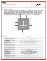
3 NTIM and OBM
1. Overview 2. Programming Sequence. 3. NTIM and OBM - Marvell
1. Overview 2. Programming Sequence. 3. NTIM and OBM - Marvell

You also want an ePaper? Increase the reach of your titles
YUMPU automatically turns print PDFs into web optimized ePapers that Google loves.
,<br />
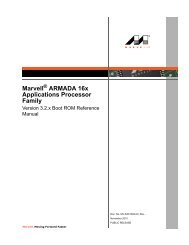
APPLICATION NOTE<br />
ARMADA 16X Memory Controller Configuration <strong>and</strong> Tuning<br />
1. Overview<br />
The ARMADA 16x Memory Controller Unit (MCU) supports LPDDR1, DDR2, <strong>and</strong> LVDDR2. It does not support LPDDR2. It is<br />
critical that the MCU be programmed correctly to ensure system stability.<br />
2. Programming Sequence.<br />
The ARMADA 16x Applications Processor Family Software Manual (MV-S301544-00) lists the order in which the MCU registers<br />
must be programmed. The Marvell OEM Boot Module (<strong>OBM</strong>) contains sample code that sets up the MCU.<br />
3. <strong>NTIM</strong> <strong>and</strong> <strong>OBM</strong><br />
On bootup, the Boot ROM loads the <strong>OBM</strong> from storage memory to internal SRAM <strong>and</strong> h<strong>and</strong>s control to it. The <strong>OBM</strong> reads<br />
content of the Non-Trusted Image Module (<strong>NTIM</strong>) <strong>and</strong> searches for a DDR configuration package. If one exists, the <strong>OBM</strong> uses<br />
the information in the <strong>NTIM</strong> to configure the MCU. The <strong>NTIM</strong> can be customized for specific DDR devices by changing the<br />
register values. The sequence in which these registers are arranged in the <strong>NTIM</strong> description file is the same sequence in which<br />
these registers are programmed by <strong>OBM</strong>. The following is an example section of the <strong>NTIM</strong> Descriptor file that relates to DDR<br />
configuration.<br />
http://www.marvell.com<br />
Copyright © 2011 Marvell Doc. No. MV-S301989-00 Rev. A<br />
January 2011, PUBLIC RELEASE Page 1
ARMADA 16X Memory Controller Configuration <strong>and</strong> Tuning<br />
Figure 1: Section of <strong>NTIM</strong> Description File Concerning DDR<br />
DDR Custom:<br />
ASPEN_SDRCTLREG13_ID: 0x0000000F<br />
ASPEN_ADRMAPREG0_ID: 0x000C0001<br />
ASPEN_SDRCFGREG0_ID: 0x00042430<br />
ASPEN_SDRTMGREG1_ID: 0x511D00C8<br />
ASPEN_SDRTMGREG2_ID: 0x74780442<br />
ASPEN_SDRTMGREG3_ID: 0x20C84A53<br />
ASPEN_SDRTMGREG4_ID: 0x36E8D8D6<br />
ASPEN_SDRTMGREG5_ID: 0x00160131<br />
ASPEN_SDRCTLREG1_ID: 0x00000000<br />
ASPEN_SDRCTLREG2_ID: 0x00080000<br />
ASPEN_SDRCTLREG3_ID: 0xc0000000<br />
ASPEN_SDRCTLREG4_ID: 0x2081C004<br />
ASPEN_SDRCTLREG6_ID: 0x00000001<br />
ASPEN_SDRCTLREG7_ID: 0x02000001<br />
Configuration<br />
Timing<br />
SDRAM Control<br />
ASPEN_PHYCTLREG11_ID: 0x00000000<br />
ASPEN_PHYCTLREG14_ID: 0x80000000<br />
ASPEN_PHYCTLREG7_ID: 0x177C2779<br />
ASPEN_PHYCTLREG8_ID: 0x07700770<br />
ASPEN_PHYCTLREG9_ID: 0x00000011<br />
…<br />
ASPEN_USRCMDREG0_ID: 0x00000001<br />
ASPEN_OPREAD_ID: 0x00000000<br />
ASPEN_OPREAD_ID: 0x00000004<br />
…<br />
ASPEN_OPREAD_ID: 0x000000fc<br />
CMCC_CONFIG_ENA_ID: 0x00000000<br />
CMCC_MEMTEST_ENA_ID: 0x00000000<br />
CMCC_CONSUMER_ID: 0x4F424D49<br />
Phy Control<br />
Start the DRAM Initialization<br />
Dummy reads to allow PLL to Update properly<br />
Memory Controller Configuration for BootRom only<br />
Config_ENA enables/disables memory configuration by bootRom<br />
MEMTEST_ENA enables/disables memory test in the bootRom<br />
CONSUMER_ID 0x4F424D49 is ASCII for <strong>OBM</strong>I<br />
An <strong>NTIM</strong> binary can be generated from the <strong>NTIM</strong> description file using the latest WTPTP release package available on the<br />
Marvell extranet at:<br />
My Products/Cellular & H<strong>and</strong>held Solutions/Applications Processors/ARMADA 16x (ARMADA 16x - 88AP16X)/<br />
Software > WTPTP<br />
Specifically, the WTPTP NTTBBV4.exe tool is used to generate the <strong>NTIM</strong> binary (see Figure 2).<br />
Figure 2:<br />
Generating the <strong>NTIM</strong> binary<br />
<strong>NTIM</strong>.txt<br />
NTTBBV4.exe<br />
<strong>NTIM</strong>.bin<br />
Alternatively, an existing <strong>NTIM</strong> binary can be modified using a hex editor. Figure 3: "Example DDR Package within the <strong>NTIM</strong><br />
Binary File" shows the DDR information in the <strong>NTIM</strong> binary. Starting at address 0x110 (in Figure 3) is a list of ID/value MCU<br />
register pairs. For convenience, the registers IDs are shown on the right side of Figure 3.<br />
Ensure the file size is not altered if editing the binary <strong>NTIM</strong> file..<br />
Doc. No. MV-S301989-00 Rev. A Copyright © 2011 Marvell<br />
Page 2 January 2011 PUBLIC RELEASE
ARMADA 16X Memory Controller Configuration <strong>and</strong> Tuning<br />
Figure 3:<br />
Example DDR Package within the <strong>NTIM</strong> Binary File<br />
<strong>NTIM</strong> <strong>and</strong> <strong>OBM</strong> are OS-agnostic. <strong>OBM</strong> can be compiled on a Windows XP machine or on a Linux machine. To compile <strong>OBM</strong>,<br />
the Software Development Suite (SDT) is needed <strong>and</strong> is available here:<br />
My Products/Cellular & H<strong>and</strong>held Solutions/Development Tools/General/C++ SDT<br />
The following sections explain how to arrive at the register values.<br />
Copyright © 2011 Marvell Doc. No. MV-S301989-00 Rev. A<br />
January 2011, PUBLIC RELEASE Page 3
ARMADA 16X Memory Controller Configuration <strong>and</strong> Tuning<br />
4. Configuration Registers<br />
SDRAM_CNTRL_13<br />
MEMORY_ADDRESS_MAP_REG0<br />
SDRAM_CONFIG_0<br />
These registers configure the size of the DDR device (that is, 128MB, 256MB), number of banks, number of rows <strong>and</strong> columns<br />
as well as drive strength <strong>and</strong> on-die termination. Partial self-refresh for LPDDR1 can also be configured.<br />
The Excel spreadsheet that complements this app note can be used to calculate registers SDRAM_CONFIG_0 <strong>and</strong><br />
MEMORY_ADDRESS_MAP_REG0.<br />
The specification sheet of a DDR device contains the necessary information to configure these registers.<br />
5. Timing Registers<br />
SDRAM_TIMING_1/2/3/4/5<br />
The specification sheet of a DDR device contains the timing values needed for proper operation. These values typically are<br />
listed in nanoseconds (ns) or number of data clock cycles (tCK). The ARMADA 16x MCU accepts those timings in number of<br />
data clocks only, so conversion is necessary if specified in fractions of a second.<br />
Example:<br />
At 200 MHz clock, one data clock cycle = 5 ns<br />
At 400 MHz clock, one data clock cycle = 2.5 ns<br />
So if the spec requires tRTP to be a minimum of 7.5 ns, then<br />
At 200 MHz clock, program the SDRAM_Config0[tRTP] with 2<br />
At 400 MHz clock, program the SDRAM_Config0[tRTP] with 3<br />
The Excel spreadsheet that complements this app note can be used to calculate the values for all the timing registers. The<br />
following three diagrams show the meaning of the timing fields used by the MCU in the ARMADA 16X Applications Processor.<br />
Doc. No. MV-S301989-00 Rev. A Copyright © 2011 Marvell<br />
Page 4 January 2011 PUBLIC RELEASE
ARMADA 16X Memory Controller Configuration <strong>and</strong> Tuning<br />
Figure 4: Timing Diagram 1<br />
BL<br />
tCCD_ccs_ext_dly<br />
trwd_ext_dly<br />
Data<br />
DR0<br />
DR1 DR2 DW0<br />
tCCD + tCCD_ccs_ext_dly<br />
tRP tRCD tCCD tRTP<br />
tCCD + trwd_ext_dly + 1<br />
CMD<br />
BA<br />
PRE ACT RD RD PRE RD WR ACT<br />
a a a a a b<br />
b a<br />
CSn0<br />
CSn1<br />
tRC<br />
Figure 5: Timing Diagram 2<br />
tCCD_ccs_wr _ext_dly<br />
tWTR<br />
Data<br />
DW0<br />
DW1<br />
DW2<br />
tRRD<br />
tCCD<br />
tCCD + tCCD_ccs_wr_ext_dly<br />
CMD<br />
BA<br />
ACT ACT WR ACT WR ACT WR<br />
RD<br />
a b a c b d c<br />
d<br />
CSn0<br />
CSn1<br />
Copyright © 2011 Marvell Doc. No. MV-S301989-00 Rev. A<br />
January 2011, PUBLIC RELEASE Page 5
ARMADA 16X Memory Controller Configuration <strong>and</strong> Tuning<br />
Figure 6: Timing Diagram 3<br />
tWR<br />
Data<br />
tRFC<br />
tRC<br />
DW0<br />
DW1<br />
DW2<br />
DW3<br />
CMD<br />
RE F ACT ACT ACT WR ACT WR WR PRE<br />
WR<br />
ACT<br />
ACT<br />
WR<br />
BA<br />
a<br />
b<br />
c<br />
a<br />
d<br />
b<br />
c<br />
a<br />
d<br />
a<br />
e<br />
e<br />
tFAW<br />
6. Control Registers<br />
SDRAM_CNTRL_1/2/3/4/5/6/7<br />
These registers control automatic power saving, automatic clock stopping (LPDDR1 only), DLL resetting (DDR2 only), SDRAM<br />
line boundary (set to line_64), auto-precharging, Powerdown mode (DDR2 only), refresh posting enabling, fast <strong>and</strong> early write<br />
enabling, data width on the DDR device, SDRAM type (DDR1 or DDR2), CAS latency, burst length, fast/normal bank<br />
addressing, arbiter master weights for the four masters, pad termination mode for Reads, <strong>and</strong> On-die termination for Read <strong>and</strong><br />
Write operations.<br />
Refer to the ARMADA 16x Applications Processor Hardware Manual (MV-S301545-00) for details.<br />
The Excel spreadsheet that complements this app note can be used to determine the register values for the SDRAM_CNTRL_4<br />
<strong>and</strong> SDRAM_CNTRL_7.<br />
7. PHY Registers <strong>and</strong> Tuning<br />
PHY_CNTRL_3/7/8/9/10/11/12/13/14<br />
The ARMADA 16x DDR PHY is a universal PHY (U-PHY). Adjust the driver strength <strong>and</strong> termination for DQ/DQS (data <strong>and</strong><br />
data strobe), ADCM (Address <strong>and</strong> comm<strong>and</strong>), <strong>and</strong> CK (clock) to obtain optimal functionality. Tune the DDR PHY for either signal<br />
integrity (recommended) or for low power.<br />
7.1 Optimal Signal Integrity Tuning<br />
This approach adjusts for optimal <strong>and</strong> quantifiable signal integrity using an oscilloscope.<br />
The goal is to have as steep as possible signal rise <strong>and</strong> fall times on the ARMADA 16x side with no under- or overswing on the<br />
signal. This procedure must be verified with a high-speed capable (active or passive) scope probe.<br />
In the simplest case, connect a 50-ohm coax cable to the scope with 50-ohm termination. On the other end, connect the cable<br />
to the signal of interest via a 500- or 1000-ohm resistor. The ARMADA 16x drive strength is set up in a similar fashion but with<br />
the scope probe on the memory side of the signal. The signal strength is increased until under- <strong>and</strong> over-swing is observed.<br />
Each of the signals to the DDR memory can be adjusted to match the impedance of the transmission lines or traces to the DDR<br />
memory. To compensate for voltage <strong>and</strong> temperature, an external resistor is used to calibrate the driver impedance.<br />
Each input signal from the DDR to the PHY can be terminated internally within the PHY. The impedance of the termination is<br />
adjustable to match the source impedance of the DDR.<br />
Doc. No. MV-S301989-00 Rev. A Copyright © 2011 Marvell<br />
Page 6 January 2011 PUBLIC RELEASE
ARMADA 16X Memory Controller Configuration <strong>and</strong> Tuning<br />
Note<br />
Since the DQ <strong>and</strong> the DQS lines provide on-die termination (ODT), no external series or parallel termination is required<br />
on those lines for point-to-point connections. This condition would apply to systems that use only one DDR memory<br />
chip. The CK, CK#, <strong>and</strong> address <strong>and</strong> control lines require parallel termination on the DDR memory side (75 ohm<br />
typically).<br />
7.2 Low Power Tuning<br />
The goal here is to use minimal drive strength <strong>and</strong> thus power consumption at the possible expense of signal integrity, which<br />
can be performed without a scope. Start with a known working drive setting on the ARMADA 16x <strong>and</strong> memory side. After writing<br />
a pattern to memory, the DDR Controller is re-initialized with lower memory drive strength <strong>and</strong> the data is read back <strong>and</strong><br />
checked for errors. If no errors occur, the drive strength can be reduced further. This procedure is repeated until Read failure<br />
occurs. When this level of drive has been reached on the memory side, the drive strength must be increased to the next higher<br />
level.<br />
Starting again from a known working drive-strength setting on the ARMADA 16x <strong>and</strong> memory side, the drive strength on the<br />
ARMADA 16x side is reduced one step at a time. Next, a pattern is written to memory <strong>and</strong> read back to check for errors. The<br />
drive strength is reduced until errors occur. At this point, the drive strength must be increased by one step. The signal margin<br />
obtained by this tuning approach is harder to quantify than using the scope-tuning approach.<br />
7.3 Read DLL<br />
The DLL <strong>and</strong> the associated delay chain are used to delay the input data strobe (DQS) so that it aligns at the center of the data<br />
(DQ), resulting in a maximally balanced setup <strong>and</strong> hold time. Ninety-degrees phase shift is recommended but values between<br />
45 to 135 degrees can be used.<br />
Figure 7:<br />
Phase Shifting DQS by 90 Degrees<br />
To calibrate the DLLs, it is essential that the preferred DDR clock speed be set <strong>and</strong> stabilized before the calibration is enabled.<br />
The master DLL is continuously calibrating itself to determine the proper delay value for a 90-degree phase shift. The result of<br />
the master DLL calibration is provided in PHY_CNTRL_14[15:8]. If PHY_CNTRL_13[Dll_auto_manual_update_en] is set then<br />
the master DLL auto calibration delay value is used, along with the preferred phase values in PHY_CNTRL_13 <strong>and</strong><br />
Copyright © 2011 Marvell Doc. No. MV-S301989-00 Rev. A<br />
January 2011, PUBLIC RELEASE Page 7
ARMADA 16X Memory Controller Configuration <strong>and</strong> Tuning<br />
PHY_DLL_CNTRL_1, to control/update the two slave DQS DLLs (DQ[7:0] <strong>and</strong> DQ[15:0]). This update occurs only when the<br />
Memory Controller has been idle for 512 cycles (see Figure 8). This is the safest “auto” method, but periodic updates are not<br />
guaranteed, especially during heavy traffic.<br />
Figure 8:<br />
DLL Control Diagram<br />
7.4 Drive Strength <strong>and</strong> Pad Termination Control on ARMADA 16x Devices<br />
LPDDR1 devices typically provide drive strengths of normal, half, quarter, <strong>and</strong> eight. DDR2 devices provide drive strengths of<br />
full or reduced. This drive strength is set up in SDRAM_CONFIG_0[ODS] <strong>and</strong> communicated to the memory device during<br />
initialization of the DDR Memory Controller (see latest DDR setup example code).<br />
ZPDRV <strong>and</strong> ZNDRV control the PMOS <strong>and</strong> NMOS coarse drive strength, <strong>and</strong> are used when the output enable (OE) is enabled,<br />
which means the PHY is driving this signal. During this time, only one side (either PMOS or NMOS) is driving at any given time.<br />
There are eight total mini-drivers (fingers) on each side. Bit 0 enables four fingers, Bit 1 enables two, <strong>and</strong> Bits 3 <strong>and</strong> 2 both<br />
enable one each. Thus, drive strength does not increase linearly with ZPDRV <strong>and</strong> ZNDRV.<br />
Doc. No. MV-S301989-00 Rev. A Copyright © 2011 Marvell<br />
Page 8 January 2011 PUBLIC RELEASE
ARMADA 16X Memory Controller Configuration <strong>and</strong> Tuning<br />
Figure 9:<br />
Pad Termination <strong>and</strong> Drive Control<br />
SDRAM_CNTRL_7[pad_term_switch_mode] controls whether pad termination is on or off. When on, ZPTRM <strong>and</strong> ZNTRM in<br />
PHY_CNTRL_7 <strong>and</strong> PHY_CNTRL_8 control the pad termination strength. When the output enable (OE) is disabled, the drivers<br />
on both sides (ARMADA 16x <strong>and</strong> DDR device) are turned on according to ZPTRM <strong>and</strong> ZNTRM, resulting in a parallel<br />
termination. The finger control scheme is similar to ZPDRV <strong>and</strong> ZNDRV.<br />
ZPR <strong>and</strong> ZNR are fine-tuning drivers. The higher the value, the lower the resistance of each finger (stronger drive strength). ZD<br />
is added on top of ZPR <strong>and</strong> ZNR, resulting in a range of 0 (equivalent to three-state, ZD=0 <strong>and</strong> ZPR/ZNR=0) to 16 (maximum<br />
per-finger strength, ZD=1 <strong>and</strong> ZPR/ZNR=15). Higher values are recommended for higher loads.<br />
Data <strong>and</strong> data strobe (DQ/DQS), address/comm<strong>and</strong> (ADCM), <strong>and</strong> clock (CK) all have separate controls. CK <strong>and</strong> ADCM share<br />
the same Z*DRV <strong>and</strong> Z*TRM values. Table 1 maps the signal controls to the correct PHY registers.<br />
Table 1:<br />
Mapping Signal Drive <strong>and</strong> Termination Strength to PHY Registers<br />
Z*DRV Z*TRM ZPR ZNR ZD<br />
PHY_CNTRL_7 DQ/DQS DQ/DQS DQ/DQS DQ/DQS DQ/DQS<br />
PHY_CNTRL_8 ADCM/CK ADCM/CK ADCM ADCM ADCM<br />
PHY_CNTRL_9 -- -- CK CK CK<br />
Table 2:<br />
Example Drive Strengths<br />
DDR Type ZPDRV ZNDRV ZPTRM ZNTRM<br />
Impedance Match (~50 ohms driving, no termination) 0011 0011 0 0<br />
DDR1 (~30 ohms driving, termination on PCB) 1111 1111 0 0<br />
DDR2 (~35 ohms driving, on-die 150 ohms<br />
termination to VDDQ <strong>and</strong> GND)<br />
0111 0111 1100 10<br />
Copyright © 2011 Marvell Doc. No. MV-S301989-00 Rev. A<br />
January 2011, PUBLIC RELEASE Page 9
ARMADA 16X Memory Controller Configuration <strong>and</strong> Tuning<br />
7.5 On-Die Termination<br />
On-Die Termination (ODT) is used with DDR2 <strong>and</strong> not with LPDDR1. For LPDDR1, the ARMADA 16x ODT must be switched<br />
off.<br />
For LPDDR1, ODT must be off:<br />
SDRAM_CONFIG_0[RTT] = 0,<br />
SDRAM_CNTRL_7[ODT0_switch_mode] = 0 (for Chip Select 0)<br />
SDRAM_CNTRL_7[ODT1_switch_mode] = 0 (for Chip Select 1)<br />
For DDR2, ODT must be on:<br />
SDRAM_CONFIG_0[RTT] = see Spec sheet for specific DDR2 device<br />
SDRAM_CNTRL_7[ODT0_switch_mode] = 0x1 or 0x2 (for Chip Select 0)<br />
SDRAM_CNTRL_7[ODT1_switch_mode] = 0x1 or 0x2 (for Chip Select 1)<br />
The RTT value is communicated to the DDR device during initialization.<br />
An ODT0_switch_mode = 0x1 means ODT is enabled for all Reads <strong>and</strong> Writes (recommended).<br />
An ODT0_switch_mode = 0x2 means ODT is by SDRAM_CNTRL_6[ODT0_write_en] <strong>and</strong> SDRAM_CNTRL_6[ODT0_read_en].<br />
This mode typically is used in a multi-chip-select system.<br />
7.6 Receiver Type <strong>and</strong> Voltage Reference<br />
This reference applies only to DQ <strong>and</strong> DQS lines, since the clock, the address <strong>and</strong> comm<strong>and</strong>, <strong>and</strong> mode pins are outputs only.<br />
Three options exist: internal reference, external reference, <strong>and</strong> DQSb. The external reference voltage is a good default choice.<br />
For receiver type, the CMOS receiver can be used as default for both DQS <strong>and</strong> DQ. However, the differential provides the best<br />
signal integrity at high speed. When using the differential receiver, the external reference voltage should be used for DQ <strong>and</strong><br />
DQS# as reference voltage for DQS.<br />
8. Entering <strong>and</strong> Exiting Self-Refresh Mode<br />
Entering Self-Refresh mode:<br />
1. Set PMUA_MC_SW_SLP_TYPE[MC_SW_SLP_TYPE] = 0 to select Self-Refresh as the sleep type of the Memory<br />
Controller.<br />
2. Set PMUA_MC_SLP_REQ[MC_SLP_REQ_MOH] = 1 to request entering Self-Refresh mode.<br />
3. Poll PMUA_MC_SLP_REQ[MC_SLP_REQ_ACK] until this bit is set. This confirms the Memory Controller is in Self-<br />
Refresh mode.<br />
Exiting Self-Refresh mode:<br />
1. Set PHY_CNTRL_14[Phy_sync_en].<br />
2. (DDR2 only) set SDRAM_CNTRL_1[DLL_reset] to reset DRAM DLL (requires mode-register update).<br />
3. (DDR2 only) set USER_INITIATED_COMMAND[user_Imr0_req] to send MRS comm<strong>and</strong>.<br />
4. (DDR2 only) Clear SDRAM_CNTRL_1[DLL_reset].<br />
5. Set PHY_CNTRL_13[dll_reset_timer] = 0x8 (2048 cycles).<br />
6. PHY_CNTRL_14[Phy_DLL_RST] to reset the PHY DLL. This blocks access to the controller for 2048 cycles.<br />
7. Set PHY_CNTRL_14[update_en_static] <strong>and</strong> wait at least 512 DCLK cycles. This forces an update to the DQS slave DLLs.<br />
8. Set PHY_CNTRL_14[update_en_static] again (this is a 1-to-toggle bit).<br />
9. Set PMUA_MC_SW_SLP_TYPE[MC_SW_SLP_TYPE] = 0 to select Self-Refresh as the sleep type of the Memory<br />
Controller.<br />
10. Set PMUA_MC_SLP_REQ[MC_SLP_REQ_MOH] = 0 to request exist from Self-Refresh mode.<br />
Doc. No. MV-S301989-00 Rev. A Copyright © 2011 Marvell<br />
Page 10 January 2011 PUBLIC RELEASE
ARMADA 16X Memory Controller Configuration <strong>and</strong> Tuning<br />
11. Poll PMUA_MC_SLP_REQ[MC_SLP_REQ_ACK] until this bit is cleared. This confirms the Memory Controller is out of lowpower<br />
mode.<br />
9. DDR Testing<br />
The <strong>OBM</strong> does not contain test code. Marvell suggests developing code that tests for the following:<br />
• Connectivity<br />
• Memory retention<br />
• Stress<br />
• Performance<br />
Disclaimer<br />
No part of this document may be reproduced or transmitted in any form or by any means, electronic or mechanical, including photocopying <strong>and</strong> recording, for any purpose, without the express<br />
written permission of Marvell. Marvell retains the right to make changes to this document at any time, without notice. Marvell makes no warranty of any kind, expressed or implied, with regard<br />
to any information contained in this document, including, but not limited to, the implied warranties of merchantability or fitness for any particular purpose. Further, Marvell does not warrant the<br />
accuracy or completeness of the information, text, graphics, or other items contained within this document.<br />
Marvell products are not designed for use in life-support equipment or applications that would cause a life-threatening situation if any such products failed. Do not use Marvell products in these<br />
types of equipment or applications.<br />
With respect to the products described herein, the user or recipient, in the absence of appropriate U.S. government authorization, agrees:<br />
1) Not to re-export or release any such information consisting of technology, software or source code controlled for national security reasons by the U.S. Export Control Regulations ("EAR"), to<br />
a national of EAR Country Groups D:1 or E:2;<br />
2) Not to export the direct product of such technology or such software, to EAR Country Groups D:1 or E:2, if such technology or software <strong>and</strong> direct products thereof are controlled for national<br />
security reasons by the EAR; <strong>and</strong>,<br />
3) In the case of technology controlled for national security reasons under the EAR where the direct product of the technology is a complete plant or component of a plant, not to export to EAR<br />
Country Groups D:1 or E:2 the direct product of the plant or major component thereof, if such direct product is controlled for national security reasons by the EAR, or is subject to controls under<br />
the U.S. Munitions List ("USML").<br />
At all times hereunder, the recipient of any such information agrees that they shall be deemed to have manually signed this document in connection with their receipt of any such information.<br />
Copyright © 2011. Marvell International Ltd. All rights reserved. Marvell, the Marvell logo, Moving Forward Faster, Alaska, Fastwriter, Datacom Systems on Silicon, Libertas, Link Street, NetGX,<br />
PHYAdvantage, Prestera, Raising The Technology Bar, The Technology Within, Virtual Cable Tester, <strong>and</strong> Yukon are registered trademarks of Marvell. Ants, AnyVoltage, Discovery, DSP<br />
Switcher, Feroceon, GalNet, GalTis, Horizon, Marvell Makes It All Possible, RADLAN, UniMAC, <strong>and</strong> VCT are trademarks of Marvell. All other trademarks are the property of their respective<br />
owners.<br />
Marvell Semiconductor, Inc.<br />
5488 Marvell Lane<br />
Santa Clara, CA 95054, USA<br />
Tel: 1.408.222.2500<br />
Fax: 1.408.752.9028<br />
Email: commsales@marvell.com<br />
www.marvell.com<br />
Copyright © 2011 Marvell Doc. No. MV-S301989-00 Rev. A<br />
January 2011, PUBLIC RELEASE Page 11