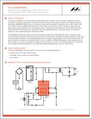
Marvell ARMADA 16x Applications Processor Family
Marvell ARMADA 16x Applications Processor Family
Marvell ARMADA 16x Applications Processor Family

Create successful ePaper yourself
Turn your PDF publications into a flip-book with our unique Google optimized e-Paper software.
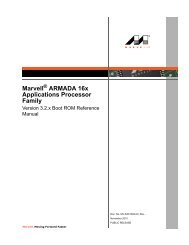
<strong>Marvell</strong> ® <strong>ARMADA</strong> <strong>16x</strong> <strong>Applications</strong> <strong>Processor</strong> <strong>Family</strong> Hardware Manual<br />
Table 7:<br />
Voltage, Temperature, and Frequency Electrical Specifications (Continued)<br />
Symbol Description Min Typical Max Units Notes<br />
NOTE:<br />
1. Minimum/maximum junction temperature depends on SKU<br />
2. The case temperature spec for <strong>Marvell</strong> ® <strong>ARMADA</strong> <strong>16x</strong> <strong>Applications</strong> <strong>Processor</strong> <strong>Family</strong> is a function of the Ψjt value<br />
that varies pending OEM system configuration. Ψjt value should be modeled and/or tested for each system<br />
configuration.<br />
3. Allowable case temperature should be calculated using following formula. Maximum Ψjt can be used for maximum<br />
allowable case temperature calculation where testing or modeling resources are nor available or system can absorb the<br />
extra guard band introduced using max Ψjt values<br />
4. Tcase (max) = Tj (max) - Ψjt * P (max)<br />
5. Tcase (max) = Maximum allowable case temperature (°C).<br />
6. Tj (max) = Maximum allowable junction temperature (°C)<br />
7. P (max) = Maximum Sustainable <strong>ARMADA</strong> Power (W)<br />
8. System design must ensure that the device case temperature is maintained within the specified limits. In some system<br />
applications it may be necessary to use external thermal management (for example, a package-mounted heat<br />
spreader) or configure the device to limit power consumption and maintain acceptable case temperatures.<br />
9. The voltage ranges specified for VDD_CORE are the targeted voltage ranges for the product. These ranges may<br />
extend or narrow depending on actual product performance and product SKUs. <strong>Marvell</strong> recommends that extended<br />
voltage and current capabilities be designed into the power management IC to accommodate future changes to this<br />
specification without requiring changes to the power management IC.<br />
10. Maximum allowable operating voltage on VDD_CORE.<br />
11. Maximum allowable voltage on VDD_CORE to meet maximum 1.4 W Pmax<br />
12. Mode 0 is PCLK = 156 MHz and DCLK = 156 MHz<br />
13. Mode 1 is PCLK = 400 MHz and DCLK = 200 MHz<br />
14. Mode 2 is PCLK = 624 MHz and DCLK = 312 MHz<br />
15. Mode 2.3 is PCLK = 624 MHz and DCLK = 156 MHz<br />
16. Mode 3 is PCLK = 800 MHz and DCLK = 400 MHz<br />
17. Mode 3.1 is PCLK = 800 MHz and DCLK = 200 MHz<br />
18. Mode 4 is PCLK = 1.066 GHz and DCLK = 533 MHz<br />
19. Mode 4.1 is PCLK = 1.066 GHz and DCLK = 355 MHz<br />
20. Maximum VDD_CORE power (Pmax) is 1.5W<br />
21. Maximum full chip power (Pmax_fullchip) is 2.0W<br />
22. Maximum full chip power (Pmax_fullchip) is 1.9W.<br />
Doc. No. MV-S301545-00 Rev. - Copyright © 2010 <strong>Marvell</strong><br />
Page 32<br />
November 2010 PUBLIC RELEASE