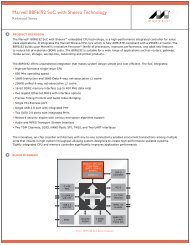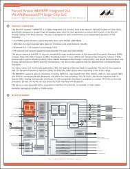
Marvell ARMADA 16x Applications Processor Family
Marvell ARMADA 16x Applications Processor Family
Marvell ARMADA 16x Applications Processor Family

Create successful ePaper yourself
Turn your PDF publications into a flip-book with our unique Google optimized e-Paper software.
<strong>Marvell</strong> ® <strong>ARMADA</strong> <strong>16x</strong> <strong>Applications</strong> <strong>Processor</strong> <strong>Family</strong> Hardware Manual<br />
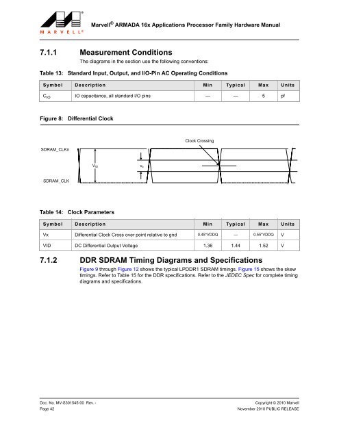
7.1.1 Measurement Conditions<br />
Table 13:<br />
The diagrams in the section use the following conventions:<br />
Standard Input, Output, and I/O-Pin AC Operating Conditions<br />
Symbol Description Min Typical Max Units<br />
C IO IO capacitance, all standard I/O pins — — 5 pf<br />
Figure 8:<br />
SDRAM_CLKn<br />
SDRAM_CLK<br />
Table 14:<br />
Differential Clock<br />
Clock Parameters<br />
V ID v x<br />
Clock Crossing<br />
Symbol Description Min Typical Max Units<br />
Vx Differential Clock Cross over point relative to gnd 0.45*VDDQ — 0.55*VDDQ V<br />
VID DC Differential Output Voltage 1.36 1.44 1.52 V<br />
7.1.2 DDR SDRAM Timing Diagrams and Specifications<br />
Figure 9 through Figure 12 shows the typical LPDDR1 SDRAM timings. Figure 15 shows the skew<br />
timings. Refer to Table 15 for the DDR specifications. Refer to the JEDEC Spec for complete timing<br />
diagrams and specifications.<br />
1<br />
2<br />
3<br />
4<br />
5<br />
6<br />
7<br />
8<br />
9<br />
10<br />
11<br />
12<br />
13<br />
14<br />
15<br />
16<br />
17<br />
18<br />
19<br />
20<br />
21<br />
22<br />
23<br />
24<br />
25<br />
26<br />
27<br />
28<br />
29<br />
30<br />
31<br />
32<br />
33<br />
34<br />
35<br />
36<br />
37<br />
38<br />
39<br />
40<br />
41<br />
42<br />
43<br />
44<br />
45<br />
46<br />
47<br />
48<br />
49<br />
50<br />
51<br />
52<br />
53<br />
54<br />
55<br />
56<br />
57<br />
58<br />
Doc. No. MV-S301545-00 Rev. -<br />
Page 42<br />
Copyright © 2010 <strong>Marvell</strong><br />
November 2010 PUBLIC RELEASE