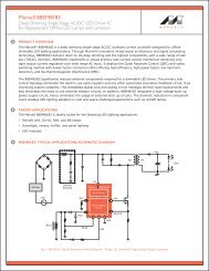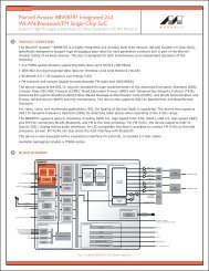
Marvell ARMADA 16x Applications Processor Family
Marvell ARMADA 16x Applications Processor Family
Marvell ARMADA 16x Applications Processor Family

You also want an ePaper? Increase the reach of your titles
YUMPU automatically turns print PDFs into web optimized ePapers that Google loves.
<strong>Marvell</strong> ® <strong>ARMADA</strong> <strong>16x</strong> <strong>Applications</strong> <strong>Processor</strong> <strong>Family</strong> Hardware Manual<br />
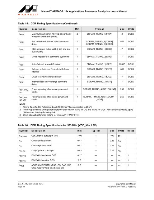
Table 15:<br />
t FAW<br />
t XSR<br />
t CKE<br />
Maximum number of ACTIVE or per-bank<br />
refreshes within this period.<br />
Self refresh exit to next valid command<br />
delay<br />
CKE minimum pulse width (High and low<br />
pulse width)<br />
2 SDRAM_TIMING_5[tFAW] 2 DCLK<br />
1 SDRAM_TIMING_3[tXSNR]<br />
SDRAM_TIMING_3[tXSRD]<br />
511 DCLK<br />
1 SDRAM_TIMING_4[tCKE] 7 DCLK<br />
t MRD Mode Register Set command cycle time 1 SDRAM_TIMING_2[tMRD] 7 DCLK<br />
t REFI Auto-Refresh Interval Counter 1 SDRAM_TIMING_1[tREFI] 65535 FCLK<br />
t RFC<br />
Refresh to Active or Refresh to Refresh<br />
internal<br />
1 SDRAM_TIMING_2[tRFC] 511 DCLK<br />
t CCD CAS# to CAS# command delay 1 SDRAM_TIMING_1[tCCD] 7 DCLK<br />
t RTP<br />
t INIT_COU<br />
NT<br />
t INIT_COU<br />
NT_NOP<br />
DDR Timing Specifications (Continued)<br />
Symbol Description Min Typical Max Units<br />
Internal Read to Precharge command<br />
delay<br />
Power up delay after stable power and<br />
clocks<br />
Power up delay after stable power and<br />
clocks<br />
1 SDRAM_TIMING_1[tRTP] 7 DCLK<br />
1 SDRAM_TIMING_4[INIT_COUNT] 255 DCLK<br />
1 SDRAM_TIMING_4[INIT_COUNT<br />
_NOP]<br />
255 DCLK<br />
NOTE:<br />
1. Timing Specified to Reference Load (50 Ohms T line connected to 20pF)<br />
2. The setup and hold timing is for reference slew rate of 1V/ns for DQ and 1V/ns for DQS. For slower slew rates, apply<br />
100ps extra derating for setup/hold.<br />
3. Drive Strength reference setting for timing ZPR=ZNR=0111<br />
Table 16:<br />
DDR Timing Specifications for 533 MHz (VDD_M = 1.8V)<br />
Symbol Description Min Typical Max Units Notes<br />
t CK(Jitter) CLK Jitter at output pin (c-c) -100 — 100 ps<br />
t CL Clock low level width 0.47 — 0.53 t CK<br />
t CH Clock high level width 0.47 — 0.53 t CK<br />
t CK_DC Duty Cycle at output pin 0.42 — 0.53 t CK<br />
t DQTVB DQ Valid time before DQS 0.27 — — ns 1<br />
t DQTVA DQ Valid time after DQS 0.3 — — ns 1<br />
t ATVB<br />
ADDR/CMD/CNTRL (RAS, CS, CAS, WE,<br />
CKE, ADDR) Valid time before CK<br />
0.6 — — ns 1<br />
1<br />
2<br />
3<br />
4<br />
5<br />
6<br />
7<br />
8<br />
9<br />
10<br />
11<br />
12<br />
13<br />
14<br />
15<br />
16<br />
17<br />
18<br />
19<br />
20<br />
21<br />
22<br />
23<br />
24<br />
25<br />
26<br />
27<br />
28<br />
29<br />
30<br />
31<br />
32<br />
33<br />
34<br />
35<br />
36<br />
37<br />
38<br />
39<br />
40<br />
41<br />
42<br />
43<br />
44<br />
45<br />
46<br />
47<br />
48<br />
49<br />
50<br />
51<br />
52<br />
53<br />
54<br />
55<br />
56<br />
57<br />
58<br />
Doc. No. MV-S301545-00 Rev. -<br />
Page 48<br />
Copyright © 2010 <strong>Marvell</strong><br />
November 2010 PUBLIC RELEASE