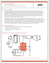
Marvell ARMADA 16x Applications Processor Family
Marvell ARMADA 16x Applications Processor Family
Marvell ARMADA 16x Applications Processor Family

You also want an ePaper? Increase the reach of your titles
YUMPU automatically turns print PDFs into web optimized ePapers that Google loves.
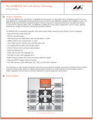
<strong>Marvell</strong> ® <strong>ARMADA</strong> <strong>16x</strong> <strong>Applications</strong> <strong>Processor</strong> <strong>Family</strong> Hardware Manual<br />
Figure 28: NAND Flash Program Timing Diagram.............................................................................................64<br />
Figure 29: NAND Flash Erase Timing Diagram .................................................................................................65<br />
Figure 30: NAND Flash Small Block Read Timing Diagram ..............................................................................65<br />
Figure 31: NAND Flash Large Block Read Timing Diagram..............................................................................66<br />
Figure 32: NAND Flash Status Read Timing Diagram.......................................................................................66<br />
Figure 33: NAND Flash ID Read Timing Diagram .............................................................................................67<br />
Figure 34: NAND Flash Reset Timing Diagram .................................................................................................67<br />
Figure 35: MultiMedia Card Timing Diagrams....................................................................................................69<br />
Figure 36: Smart Panel Interface 8-bit 8080-Series Parallel Mode Read Interface Protocol.............................71<br />
Figure 37: Smart Panel Interface 8-bit 8080-Series Parallel Mode Write Interface Protocol .............................71<br />
Figure 38: Smart Panel Interface 8-bit 6800-Series Parallel Mode Read Interface Protocol.............................72<br />
Figure 39: Smart Panel Interface 8-bit 6800-Series Parallel Mode Write Interface Protocol .............................72<br />
Figure 40: SPI Write/Read Protocol...................................................................................................................73<br />
Figure 41: Dumb LCD Panel Horizontal Timing.................................................................................................74<br />
Figure 42: Dumb LCD Panel Vertical Timing .....................................................................................................74<br />
Figure 43: Parallel Timing Diagram ...................................................................................................................76<br />
Figure 44: SSP Master Mode Timing Diagram ..................................................................................................77<br />
Figure 45: SSP Slave Mode Timing Definitions .................................................................................................78<br />
Figure 46: TWSI Output Delay AC Timing Diagram...........................................................................................79<br />
Figure 47: TWSI Output Delay AC Timing Diagram...........................................................................................79<br />
Figure 48: TWSI Test Circuit..............................................................................................................................81<br />
Figure 49: AC’97 CODEC Timing Diagram........................................................................................................82<br />
Figure 50: JTAG Interface Output Delay AC Timing Diagram ...........................................................................83<br />
Figure 51: JTAG Interface Input AC Timing Diagram ........................................................................................83<br />
Figure 52: JTAG Interface Test Circuit ..............................................................................................................84<br />
Figure 53: Low/Full Speed Data Signal Rise and Fall Time ..............................................................................85<br />
Figure 54: High Speed TX Eye Diagram Pattern Template ...............................................................................85<br />
Figure 55: High Speed RX Eye Diagram Pattern Template...............................................................................86<br />
Figure 56: MII Tx Mode Interface Timing Diagrams...........................................................................................90<br />
Figure 57: MII Rx Model Interface Timing Diagrams..........................................................................................91<br />
Figure 58: MII Management Interface Timing Diagrams....................................................................................91<br />
Figure 59: Power-Up Reset Timing....................................................................................................................94<br />
Figure 60: Powerdown Timing ...........................................................................................................................96<br />
8 Design Guidelines and Checklist ................................................................................................... 97<br />
Figure 61: Panel Power Sequence ..................................................................................................................100<br />
Figure 62: DPOT Programming Sequence ......................................................................................................101<br />
Figure 63: Source Driver Connections.............................................................................................................102<br />
Figure 64: Source Driver Timing ......................................................................................................................103<br />
Figure 65: Gate Driver Connections ................................................................................................................104<br />
Figure 66: Gate Driver Output Enable Timing..................................................................................................104<br />
Doc. No. MV-S301545-00 Rev. - Copyright © 2010 <strong>Marvell</strong><br />
Page 8<br />
November 2010 PUBLIC RELEASE