Hams in Space!
Hams in Space! - Free and Open Source Software
Hams in Space! - Free and Open Source Software
- No tags were found...

Create successful ePaper yourself
Turn your PDF publications into a flip-book with our unique Google optimized e-Paper software.
I<br />
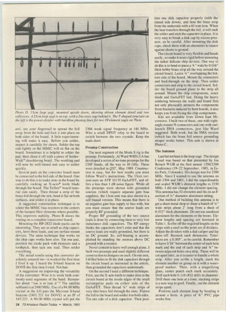
Photo D. Hem loop JW:i, mounted upside down, show<strong>in</strong>g d riven element detail and two<br />
reflectors. A 23('171 loop vagi is on top , with a 2m cross yogi beh<strong>in</strong>d it. The t -snoped structure on<br />
the left is Ihe P0\l'('T divider with hardl<strong>in</strong>e phas<strong>in</strong>g l<strong>in</strong>esfor IWO 19 element yogis on JOon.<br />
awl. use your f<strong>in</strong>gernail to spread the foil<br />
away fro m the hole and lock it <strong>in</strong>to place on<br />
both sides o f the board . A little expe riment<strong>in</strong>g<br />
will make it easy. Before you solde r,<br />
<strong>in</strong>spect it carefully for sbons, Solder the top<br />
side lightly so the MM IC will sit flat on the<br />
board. Sometimes it is hel pful to solder the<br />
pad , the n clean it o ff with a piece of Solde r<br />
wick" desolder<strong>in</strong>g braid . The result <strong>in</strong>g pad<br />
wi ll now be we ll-t<strong>in</strong>ned and easy to solde r<br />
quickly .<br />
Several pads on the conve ner board must<br />
be connected to the fo il side of the board. O ne<br />
way to do th is is to make slots <strong>in</strong> the board by<br />
carefully rock<strong>in</strong>g an X -ac to~ knife blade<br />
th rough the board . Th e Teflon" board material<br />
cuts easily . Th en thread a strip of the<br />
brass foil through the slot , bend it flat on both<br />
surfaces. and solder it <strong>in</strong> place.<br />
A suggested construction technique is to<br />
solder the MM IC bias resisto rs to the centers<br />
of the hai rpi n filter clements where possible.<br />
This improves stability . Photo B shows the<br />
rout<strong>in</strong>g on a comp lete rransverter board .<br />
Mount<strong>in</strong>g the HP-2822 d iode packs can be<br />
<strong>in</strong>terest<strong>in</strong>g . They are as sma ll as chip capacito<br />
rs, have three lead s, and are surface mount<br />
devices. Th e same technique that works on<br />
the chip caps works here also. T <strong>in</strong> one pad,<br />
position the diode pack with tweezers and a<br />
toothpick. then tack one lead . Then solder<br />
everyth<strong>in</strong>g.<br />
The <strong>in</strong>itial results us<strong>in</strong>g this convener absolutely<br />
amazed me- il worked the first time<br />
I fired it up . I heard the Scband beacon on<br />
DOVE the first time I tried. Not bad .<br />
A suggestion on improv<strong>in</strong>g the versatility<br />
of the convener: W ire it to work both commonly-used<br />
segments o f the ba nd. Reme m<br />
be r abou t " use il o r lose it"? The satellite<br />
subband is at 2400 MHz . Usc of a 94.00 MHz<br />
crystal <strong>in</strong> the LO puts the M icrosat Scband<br />
beacons (2401.221 for DO VE) at an IF of<br />
145 ,22 1. A 90.00 MH7. crystal w ill put the<br />
26 73Amateur RadioToday . March,1 991<br />
2304 weak signal freque ncy at 144 MHz.<br />
Wire a small DPDT re lay to the boa rd to<br />
switch between the IWO crystals . Keep the<br />
leads short .<br />
Preamp Consiructton<br />
The next segment of the Mode S rig is the<br />
preamp. Fortunately, AIWard WB5LUA has<br />
developed a series of no-tune preamps for the<br />
UHF bands, all the way to 10 GHz . These<br />
were detailed <strong>in</strong> QST, May 1989. Construction<br />
is easy, but for best results you must<br />
foll ow Ward' s <strong>in</strong>structions. The 13cm version<br />
uses an ATF 10135 GaAsFET, and offers<br />
a less than I dB noise figu re . While all<br />
the preamps were shown with grounded<br />
sources (w hich require sepa rate gate bias<br />
supplies), the 13cm unit was also shown <strong>in</strong> a<br />
self-biased version. This means that there is<br />
no negative gate bias supply to fuss with, but<br />
you must ensure that the sou rce leads are<br />
properly RF grou nded.<br />
Proper RF ground<strong>in</strong>g of the two sou rce<br />
leads is done by connect<strong>in</strong>g them to very low<br />
<strong>in</strong>ductance d isk capacitors. The RF energy<br />
th<strong>in</strong>ks the capacitors don' t exist and that the<br />
source leads are really grounded, but there is<br />
no DC ground . So, self-bi as<strong>in</strong>g is accomplished<br />
by stand<strong>in</strong>g the sources above DC<br />
ground with a resistor .<br />
Never content to leave well enough alone. I<br />
bu ilt two prea mps and used slightly d ifferent<br />
construction techniques on each. On one unit,<br />
I drilled holes to fit the disk capacitors through<br />
the circu it board as <strong>in</strong>structed <strong>in</strong> the art icle,<br />
then grounded the capacitors underneath .<br />
On the second I used a d iffere nt technique .<br />
First, use the Xcactc knife to male slots <strong>in</strong> the<br />
circuit board at the <strong>in</strong>side edges of the small<br />
recta ngular pad s on e ither side o f th e<br />
GaAsFET. Then thread 1.4 N wide strips of<br />
very th<strong>in</strong> brass foil th rou gh the slots. Flatten<br />
the foil to the board and solder it 10 bot h sides.<br />
T<strong>in</strong> one side of a di sk capacitor. Then position<br />
one disk capacitor properly (with the<br />
t<strong>in</strong>ned side down), and heat the brass strip<br />
from the underside with a40 wan iron. When<br />
the heal transfers through the foil, it will melt<br />
the solde r and stick the capacitor <strong>in</strong> place. It is<br />
very easy to break a disk cap by excess pressure<br />
, so be careful. After mount<strong>in</strong>g the disk<br />
caps, check them with an ohmmeter to <strong>in</strong>sure<br />
aga<strong>in</strong>st shorts to grou nd .<br />
The circuit board is very flexib le and be nds<br />
easily , so make it more rigid before mount<strong>in</strong>g<br />
the rather delicate chip devices. One way to<br />
do this is to bend or piece a :j,i N wide by 0.016"<br />
thick hobby brass strip allthe way around the<br />
circuit board . Leave 1J. N overlapp<strong>in</strong>g the bottom<br />
side of the board . Mount the connectors<br />
and feed -through on the strip. Then solder<br />
connectors and strip to the circuit board. Solde<br />
r the board ground plane to the strip all<br />
arou nd . Mount the chip components, zener<br />
diode and GaAsFET last. Do<strong>in</strong>g the heavy<br />
solder<strong>in</strong>g between the walls and board first<br />
nor only physically protects the components<br />
from fractures <strong>in</strong>duced by bent boards, it also<br />
keeps you from fry <strong>in</strong>g the chip components.<br />
Kits are ava ilable from Dow n East Microwave.<br />
I built two of these , one with right <br />
angle-mount N-connectors and one with endlaunch<br />
SMA connectors, just like Ward<br />
suggested. Both work, but the SMA ve rsion<br />
(which has the brass foil source ground<strong>in</strong>g<br />
straps) wo rks better. This un it is shown <strong>in</strong><br />
Photo C,<br />
The Antenna<br />
Last bn noc least istheloop yagi. The desi gn<br />
I used was based on that presented by Joe<br />
Reisen W IJ R at the first annual 1296/2304<br />
Conference (19- 22 September, 1985. <strong>in</strong> Esres<br />
Park , Colorado). Hi s design was for 2304<br />
MHz. S<strong>in</strong>ce I wanted to use the antenna on<br />
both 2304 and 240 1, I did the unpardonable<br />
and scaled WIJR's elem ent length s to 2350<br />
MH z . I d id not change the clement spac<strong>in</strong>g.<br />
This antenna has 52 ele ments and fits on an 8'<br />
section of Ifz · diameter alum<strong>in</strong>um tub<strong>in</strong>g.<br />
One method of buildi ng this antenna is to<br />
get a sheet metal shop to shear a bu nch of 1,4.<br />
wide strips about 2' long from a sheet of<br />
0.032- thick alum<strong>in</strong>um. Do not use anodized<br />
alum<strong>in</strong>um for the elements o r the boom. Eleme<br />
nt lengths and spac<strong>in</strong>g are itemized <strong>in</strong><br />
Table I . Scribe off the required length s on the<br />
strips with a steel scribe poi nt set ofdividers.<br />
Adjust the d ividers with a dial caliper and lay<br />
them off. Recneck each dimension . Tolerances<br />
arc ± O.OO5" , so be careful. Remember<br />
to leav e 3/ 16" between the center ofeach hole<br />
mark and the end of each strip and between<br />
adjacent holes on a strip. These will be<br />
*N<br />
cut apart later, as it is eas ier to handle a whole<br />
strip . After you scribe a length, mark the<br />
element number or groop on it with a waterproof<br />
marker. Then, wi th a magnify<strong>in</strong>g<br />
gla...s, center punch each mark accurately.<br />
Drill each hole 0 .116 (#32 drill) <strong>in</strong> diameter.<br />
Drill them o ne hole at a time; stack<strong>in</strong>g strips<br />
is a sure way to goof. F<strong>in</strong>ally, cut the clement<br />
strips apan .<br />
Preform each element loop by bendi ng it<br />
around a form . A piece of -\Ii n<br />
works f<strong>in</strong>e .<br />
PVC pipe