Powering Freight & Transportation - Power Systems Design
Powering Freight & Transportation - Power Systems Design
Powering Freight & Transportation - Power Systems Design

You also want an ePaper? Increase the reach of your titles
YUMPU automatically turns print PDFs into web optimized ePapers that Google loves.
38<br />
Solar <strong>Power</strong><br />
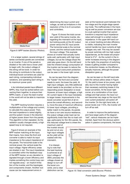
Figure 9: MPP tracker (Source: Photon).<br />
• In a larger system, several strings of<br />
series-connected panels are connected<br />
to an inverter. If one of the panels is<br />
shaded or the cells have a lower yield<br />
to begin with, the output voltage of<br />
this string will be lower. In order for<br />
this string to contribute to the output,<br />
individual boost converters are used for<br />
each string, compensating individual<br />
variations, and operating each string in<br />
its maximum power point.<br />
• As individual panels have different<br />
MPPs, they must be sorted before connecting<br />
them together, to ensure their<br />
MPPs match, or even the best inverter<br />
in the world will not be able to maximize<br />
the yield.<br />
The MPP tracking function requires a<br />
multiplication of the voltage and current,<br />
to calculate the output power. Then,<br />
the load impedance is varied slightly,<br />
and the system moves in the direction<br />
of higher power drawn from the panels.<br />
This algorithm is then repeated. As the<br />
radiation usually changes slowly, a high<br />
speed loop is not required.<br />
Figure 9 shows an example of the<br />
MPP tracker matching at the input,<br />
that means, how close the front end<br />
converter is able to match its input<br />
impedance to the output impedance of<br />
the panels. The horizontal scale is the<br />
nominal power; the vertical scale the<br />
input voltage. Higher efficiency areas<br />
are shaded in red. The input impedance<br />
is controlled within the feedback loop<br />
of the MPP tracker, so any deviation is<br />
signaled through a lower efficiency and<br />
implies something this control loop cannot<br />
regulate away – an implicit limitation<br />
of the inverter, and the topologies<br />
and components chosen. Another root<br />
cause can be measurement errors in<br />
determining the input current and<br />
voltage, as well as limitations in the<br />
resolution of the A-to-D converters<br />
and controllers.<br />
Figure 10 shows the total conversion<br />
yield of the same inverter, disregarding<br />
the mismatch at the input,<br />
but looking purely at the AC output<br />
power versus the DC input power.<br />
The horizontal scale is the nominal<br />
power, and the vertical scale shows<br />
the input voltage. This example<br />
shows an inverter that actually works<br />
quite well, particularly with high input<br />
voltages, but as the voltage drops the<br />
yield also goes down. On the left hand<br />
side the inherent energy consumption of<br />
the inverter can be seen to reduce the<br />
yield. The input overcurrent protection<br />
can be seen in the lower right corner.<br />
As can be seen from the diagram,<br />
the “harder” the front end converter<br />
needs to work, the lower the yield. At<br />
high input voltages, very little additional<br />
boost needs to be provided, so the corresponding<br />
power dissipation is lower.<br />
However, at lower input voltages, a high<br />
AC current ripple in the input translates<br />
to larger losses. Improvements in the<br />
boost converter would first of all improve<br />
the overall efficiency, and secondly,<br />
move the area of maximum efficiency<br />
to lower input voltages, providing a<br />
better match to the panels. As panels<br />
do have a non-zero source resistance,<br />
the output voltage under load can be<br />
significantly lower than the no-load voltage,<br />
particularly for thin-film panels. So,<br />
this reduced voltage level is where the<br />
maximum yield of<br />
the inverter should<br />
be and not at very<br />
high input voltages<br />
as the yield will be<br />
wasted with this<br />
mismatch.<br />
It is interesting<br />
to note that<br />
the best tracking<br />
is achieved at an<br />
input voltage of<br />
390V, precisely the<br />
voltage chosen at<br />
design to turn-off<br />
the boost converter,<br />
and a clear<br />
distinction can be<br />
seen at the handover point between the<br />
two-stage and the single-stage operating<br />
mode. The inefficiencies in the tracking<br />
as well as power conversion are due<br />
to a sub-optimal inverter that cannot<br />
transform a required input impedance<br />
value well enough to a certain output<br />
impedance. In the upper left hand corner,<br />
a lower tracking and also efficiency<br />
is visible, indicating the main inverter<br />
cannot handle low input currents at high<br />
voltages very well. This may be caused<br />
by power switches with too high output<br />
capacitances, as the losses are proportional<br />
to C*U 2 . As the current in the inverter<br />
increases (moving in the diagram<br />
to the right), the proportion of switching<br />
losses is getting smaller compared to<br />
the conduction losses, so the efficiency<br />
actually improves, although the power<br />
dissipation goes up.<br />
As can be seen on the left hand side<br />
with the vertical yellow areas in Figure<br />
10, the yield is lower at low power, probably<br />
due to this inverter having higher<br />
than necessary switching losses in the<br />
boost converters. At the lower right<br />
corner, at a combination of low input<br />
voltage and high power, the input current<br />
becomes very large so the input DC<br />
over current protection will switch off<br />
the inverter. On the right hand side, at<br />
power levels over 115%, the inverter will<br />
turn off as well.<br />
In order to improve the performance,<br />
and have larger parts of the diagram<br />
“red”, various measures can be implemented.<br />
Apart from the obvious optimization<br />
in passive components, the boost<br />
Figure 10: Total conversion yield (Source: Photon).<br />
<strong>Power</strong> <strong>Systems</strong> <strong>Design</strong> October 2008<br />
Figure 11: The correct gate drive of the power switches is crucial in many respects.<br />
diodes need to be carefully selected<br />
for low switching losses (improving the<br />
performance at low input power, the left<br />
side of the diagram), and for low forward<br />
voltage drop (to improve the yield at<br />
high input currents, the lower part of<br />
the diagram). The StealthTM II diodes<br />
from Fairchild Semiconductor or silicon<br />
carbide diodes can provide this optimization.<br />
The power switches in the boost<br />
converter, usually MOSFETs, also need<br />
to be carefully chosen. At low input voltages,<br />
the current through the switches<br />
is causing conduction losses due to<br />
the high duty cycle, so low RDSON is<br />
important – in fact, it is not uncommon<br />
to see several large MOSFETs in TO-247<br />
packages connected in parallel.<br />
Further improvements can be gained<br />
with a careful choice of operating<br />
mode of the boost converter. Continuous<br />
mode conversion is chosen,<br />
to minimize AC losses, and the lower<br />
ripple currents allow for reduction of<br />
unwanted overhead in the system.<br />
However, this is a hard-switching<br />
system, so power MOSFETs with a<br />
low output capacitance should be<br />
chosen. This however contradicts<br />
somewhat with the requirement for low<br />
conduction losses in the switch, to be<br />
obtained with a larger device. Here,<br />
a good compromise can be found in<br />
Fairchild’s SuperFET devices that<br />
can at the same time provide a “fast”<br />
body diode at no RDSON penalty.<br />
This also helps at the lower right hand<br />
corner of the diagram, as at low input<br />
voltage and high power the duty cycle<br />
of the converter is quite long, with high<br />
www.powersystemsdesign.com<br />
currents in the switch.<br />
The value of Rgate plays a significant<br />
role in the performance of the system.<br />
The lower this resistor becomes, the<br />
faster the MOSFET will be switching<br />
(provided the gate driver has sufficiently<br />
low output impedance). Faster switching<br />
corresponds to higher dI/dt and dv/dt,<br />
increased electromagnetic emission<br />
(EMI), and can lead to breakdown of<br />
the components, reducing reliability. If<br />
the gate resistor value is increased, the<br />
switching speed is reduced, but this<br />
means the overlap between current in<br />
the device, and voltage across the device,<br />
is increased, and so are the switching<br />
losses. In other words, the switch<br />
behaves less and less as a switch, but<br />
spends more and more time in the linear<br />
region, causing power dissipation. In<br />
conclusion, the gate resistance values<br />
need to be finely tuned for lowest power<br />
dissipation and EMI.<br />
To improve performance even further,<br />
resonant or quasi-resonant topologies<br />
can be used, although they can be challenging<br />
to implement for a wide input<br />
voltage range and still operate at ZVS<br />
(“zero voltage switching”) or ZCS (“zero<br />
current switching”). Another topology to<br />
improve performance is the interleaved<br />
boost converter. Here, multiple converters<br />
are working in parallel, out-of-phase<br />
with each other, and it can be shown<br />
that the ripple current in the output can<br />
be reduced. And, if the input voltage is<br />
high enough, the boost converter can be<br />
turned off completely and bridged e.g.,<br />
with a relay, to further reduce losses.<br />
Solar <strong>Power</strong><br />
The inverter or DC-to-AC section of<br />
the inverter can be built with many different<br />
topologies, quite a few of them<br />
proprietary to some of the companies<br />
building inverters. One of the “classical”<br />
topologies consists of using a<br />
full bridge, driving output inductors to<br />
reduce EMI. Here, some of the devices<br />
can be switched at line frequency<br />
whereas others are switched with the<br />
conversion frequency – if done cleverly,<br />
the first devices can be chosen<br />
for lowest conduction losses, like the<br />
Non Punch Through(NPT) Fieldstop(FS)<br />
IGBTs from Fairchild Semiconductor,<br />
whereas the latter should be chosen for<br />
lowest switching losses, e.g. the new<br />
NPT Field Stop Trench devices from<br />
Fairchild Semiconductor. Here, a combination<br />
of different IGBTs or even IGBTs<br />
and MOSFETs can help to improve the<br />
overall yield. And to properly drive the<br />
power switches, optically isolated gate<br />
drivers like Fairchild’s FOD3180 can be<br />
used, improving the system reliability<br />
where high dv/dt can suddenly occur,<br />
e.g., in the case of a grid fault.<br />
In applications such as solar inverters,<br />
where the key performance parameter<br />
is the conversion efficiency, improvements<br />
in switching device performance,<br />
through the use of IGBTs, MOSFETs<br />
and diodes are very important. Here,<br />
the voltage drops and switching energy<br />
losses can still be improved, although in<br />
order to realize the potential gains, more<br />
brainpower has to go into how to drive<br />
the switches properly, to avoid parasitic<br />
oscillations and overvoltages: the two<br />
biggest enemies of high efficiency and<br />
robustness. Here, integration of subsystems<br />
into intelligent power modules can<br />
really help! Due to the close proximity<br />
and ideal matching of driver and power<br />
switch, the best possible switching<br />
behavior can be realized repeatedly.<br />
Fairchild Semiconductor is driving the<br />
state-of- the-art in both power switch<br />
technologies as well as module integration<br />
to support further performance<br />
improvements in these green high-tech<br />
applications.<br />
www.fairchildsemi.com<br />
39