Powering Freight & Transportation - Power Systems Design
Powering Freight & Transportation - Power Systems Design
Powering Freight & Transportation - Power Systems Design

Create successful ePaper yourself
Turn your PDF publications into a flip-book with our unique Google optimized e-Paper software.
48<br />
<strong><strong>Power</strong>ing</strong> <strong>Freight</strong> & <strong>Transportation</strong><br />
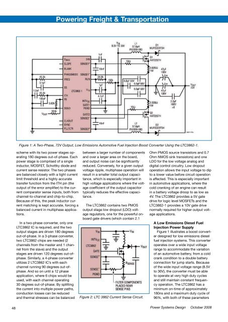
Figure 1: A Two-Phase, 72V Output, Low Emissions Automotive Fuel Injection Boost Converter Using the LTC3862-1.<br />
scheme with its two power stages operating<br />
180 degrees out-of-phase. Each<br />
power stage is comprised of a single<br />
inductor, MOSFET, Schottky diode and<br />
current sense resistor. The two phases<br />
are balanced closely with a tight current<br />
limit threshold and a highly accurate<br />
transfer function from the ITH pin (the<br />
output of the error amplifier) to the current<br />
comparator sense inputs, both from<br />
channel-to-channel and chip-to-chip.<br />
Because of this, the peak inductor current<br />
matching is kept accurate, forcing a<br />
balanced current in multiphase applications.<br />
In a two-phase converter, only one<br />
LTC3862 IC is required, and the two<br />
output stages are driven 180 degrees<br />
out-of-phase. In a 3-phase converter,<br />
two LTC3862 chips are needed (2<br />
channels from the master and 1 channel<br />
from the slave) and the output<br />
stages are driven 120 degrees out-ofphase.<br />
Similarly, a 4-phase converter<br />
utilizes 2 LTC3862 IC’s with each<br />
channel running 90 degrees out-ofphase.<br />
And so on until a 12 phase<br />
application, where 6 chips would be<br />
used, with each channel operating<br />
30 degrees out-of-phase. By splitting<br />
the current into multiple power paths,<br />
conduction losses can be reduced<br />
and thermal stresses can be balanced<br />
between a larger number of components<br />
and over a larger area on the board,<br />
and output noise can be significantly<br />
reduced. Conversely, for a given output<br />
voltage ripple, multiphase operation will<br />
result in a smaller total output capacitance,<br />
which is especially important in<br />
high voltage applications where the voltage<br />
coefficient of the output capacitor<br />
typically reduces the effective capacitance.<br />
The LTC3862 contains two PMOS<br />
output stage low dropout (LDO) voltage<br />
regulators, one for the powerful onboard<br />
gate drivers (which contain 2.1<br />
Figure 2: LTC 3862 Current Sense Circuit.<br />
Ohm PMOS source transistors and 0.7<br />
Ohm NMOS sink transistors) and one<br />
LDO for the low voltage analog and<br />
digital control circuitry. Low dropout<br />
operation allows the input voltage to dip<br />
to a lower value before circuit operation<br />
is affected. This is especially important<br />
in automotive applications, where the<br />
cold cranking of an engine can result<br />
in a battery voltage droop to as low as<br />
4V. The LTC3862 provides a 5V gate<br />
drive for logic level MOSFETs and the<br />
LTC3862-1 provides a 10V gate drive<br />
normally required for higher output voltage<br />
applications.<br />
A Low Emissions Diesel Fuel<br />
Injection <strong>Power</strong> Supply<br />
Figure 1 illustrates a boost converter<br />
designed for low emissions diesel<br />
fuel injection systems. This converter<br />
operates over a wide input voltage<br />
range to accommodate the variation<br />
of an automotive battery, from a cold<br />
crank condition to a double battery<br />
connection for jump starts. Because<br />
of the wide input voltage range (8.5V<br />
to 36V), the converter must be able<br />
to operate at very high duty cycles<br />
and still maintain constant frequency<br />
operation. The LTC3862 has a<br />
minimum on-time of approximately<br />
180ns and a maximum duty cycle of<br />
96%, with both of these parameters<br />
<strong>Power</strong> <strong>Systems</strong> <strong>Design</strong> October 2008<br />
being user programmable. The operating<br />
frequency can be programmed from<br />
75kHz to 500kHz using a single resistor,<br />
and a phase lock loop can be used<br />
to synchronize the operating frequency<br />
to an external clock source. For the<br />
example, the power MOSFETs used in<br />
Figure 1 are the HAT2267H from Renesas,<br />
a 57μH inductor with a saturation<br />
current rating of 5A, and a total output<br />
capacitance of only 107μF is necessary.<br />
The output capacitance consists of two<br />
47μF aluminum electrolytic bulk capacitors<br />
connected in parallel with six low<br />
ESR 2.2μF ceramic capacitors, in order<br />
to meet the output voltage ripple and<br />
RMS current requirements. This con-<br />
www.powersystemsdesign.com<br />
<strong><strong>Power</strong>ing</strong> <strong>Freight</strong> & <strong>Transportation</strong><br />
figuration also limits the output voltage<br />
ripple to only 500mV.<br />
This circuit operates with a peak efficiency<br />
of 96% at an input voltage of<br />
32V. Because a single-ended boost converter<br />
regulates the current in the source<br />
of the low-side switch, the maximum<br />
current that can be delivered to the<br />
load is a function of the input voltage.<br />
As a result, this converter is capable of<br />
delivering 0.5A to the load at an input of<br />
8.5V, 1.5A at an input of 24V, and 2A at<br />
an input of 32V to 36V.<br />
The LTC3862 features two pins, CLK-<br />
OUT and PHASEMODE that allow mul-<br />
Figure 3: A 12V Input, 24V/5A Output 2-Phase Car<br />
Audio <strong>Power</strong> Supply Using the LTC3862, and Its<br />
Associated Efficiency Curve.<br />
tiple ICs to be daisy-chained together<br />
for higher current multiphase applications.<br />
For a 3- or 4-phase design, the<br />
CLKOUT signal of the master controller<br />
is connected to the SYNC input of the<br />
slave controller in order to synchronize<br />
additional power stages for a single high<br />
current output. The PHASEMODE pin<br />
is used to adjust the phase relationship<br />
between channel 1 and CLKOUT, as<br />
summarized in Table 1. The phases are<br />
calculated relative to the zero degrees,<br />
defined as the rising edge of the GATE1<br />
output. In a 6-phase application, the<br />
CLKOUT pin of the master controller<br />
connects to the SYNC input of the 2nd<br />
controller and the CLKOUT pin of the<br />
49