

tidu271

You also want an ePaper? Increase the reach of your titles
YUMPU automatically turns print PDFs into web optimized ePapers that Google loves.
www.ti.com<br />
F<br />
F<br />
CM _ 1<br />
CM _ 2<br />
1<br />
<br />
2 RS1<br />
C<br />
1<br />
<br />
CM1<br />
2 RS2<br />
CCM2<br />
Theory of Operation<br />
(6)<br />
F F <br />
CM _ 1 CM _ 2 3.2 KHz<br />
(7)<br />
5.1.6 PGA Gain and Common Mode Voltage<br />
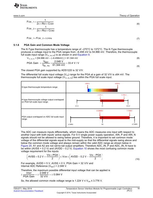
The K-Type thermocouple has a temperature range of –270°C to 1372°C. The K-Type thermocouple<br />
produces a voltage input to the PGA ranges from –6.458 mV to 54.886 mV. Therefore, the thermocouple<br />
full scale input range (V TC_IN_FS ) is as shown in and Equation 9.<br />
V TC_IN_FS = [54.886 mV – (–6.458mV) ] = 61.344 mV (8)<br />
VREF<br />
2.048 V<br />
PGA Gain 33.4 V / V<br />
VIN_FS<br />
61.344 mV<br />
(9)<br />
The closest PGA gain supported by ADS1220 is 32 V/V.<br />
The differential full scale input voltage (V FS ) range for the PGA at a gain of 32 V/V is ±64 mV. The<br />
thermocouple full scale input voltage (V TC_IN_FS ) lies within the PGA full scale input.<br />
K-type thermocouple temperature range:<br />
K-type thermocouple voltage output overlapped<br />
on PGA full scale input range:<br />
PGA output overlapped on ADC full scale input<br />
range:<br />
The ADC can measure inputs differentially, which means the ADC measures one input with respect to<br />
another input with both inputs' active signals. For 5-V single power supply operation, AIN_P and AIN_N<br />
signals should not be allowed to swing below ground. Therefore, it is important to set common mode<br />
voltage of the differential signals equal to the mid-supply so that the differential signals swing above and<br />
below the common mode voltage and always remain within the valid ADC range as shown below in<br />
Figure 20. A1 and A2 are not rail-to-rail output amplifiers. Therefore ADC_IN_P and ADC_IN_N have to<br />
be within (AVSS + 0.2 V) and (AVDD – 0.2 V). Equation 10 shows the most confusing common mode<br />
voltage requirement for the inputs:<br />
VIN<br />
PGA VIN<br />
PGA<br />
CM<br />
<br />
AVSS 0.2 V V AVDD 0.2 V <br />
2<br />
<br />
2<br />
<br />
<br />
For example, AVDD = 5 V, AVSS = 0 V, PGA Gain = 32 V/V and<br />
Internal ADC Reference (V REF ) = 2.048 V.<br />
Therefore, the maximum possible differential input voltage that can be applied is<br />
VREF<br />
2.048 V<br />
0.064 V<br />
PGA Gain<br />
32 V/V<br />
<br />
So, the allowed common mode voltage range is 1.224 V ≤ V CM ≤ 3.776 V.<br />
(10)<br />
TIDU271–May 2014<br />
Submit Documentation Feedback<br />
Temperature Sensor Interface Module for Programmable Logic Controllers<br />
(PLC)<br />
Copyright © 2014, Texas Instruments Incorporated<br />
19