Design Flow
Design Flow
Design Flow

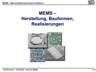
Create successful ePaper yourself
Turn your PDF publications into a flip-book with our unique Google optimized e-Paper software.
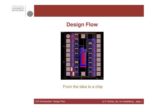
CCS Introduction: <strong>Design</strong> <strong>Flow</strong><br />
<strong>Design</strong> <strong>Flow</strong><br />
From the idea to a chip<br />
© P. Fischer, ziti, Uni Heidelberg page 1
VLSI <strong>Design</strong><br />
This lecture<br />
Levels of Abstraction<br />
System<br />
Chip<br />
Modul<br />
Gatter<br />
Schaltung<br />
Bauelement<br />
Technologie<br />
Physik<br />
CCS Introduction: <strong>Design</strong> <strong>Flow</strong><br />
Grafik<br />
CPU RAM<br />
Control<br />
ALU<br />
Register<br />
File<br />
© P. Fischer, ziti, Uni Heidelberg page 2
<strong>Design</strong> Hierarchy<br />
� Each block is divided into smaller blocks<br />
� Description via schematic or a hardware description<br />
language HDL (for digital stuff) (Verilog…)<br />
CCS Introduction: <strong>Design</strong> <strong>Flow</strong><br />
'Core'<br />
© P. Fischer, ziti, Uni Heidelberg page 3
A real design hierarchy (P6)<br />
� Many levels…<br />
� In our designs<br />
Example: Simple Digital Analog Converter<br />
Chip<br />
Core<br />
Serial Interface<br />
x-y-Decoder<br />
Current<br />
reference<br />
FFs Gatter<br />
Gatter<br />
Current sources<br />
IO Pads (CMOS in, CMOS out, Power, Analogpads)<br />
CCS Introduction: <strong>Design</strong> <strong>Flow</strong><br />
source switch<br />
Output stage<br />
© P. Fischer, ziti, Uni Heidelberg page 5
Top-Down, Bottom-Up<br />
� I think both ‚strict‘ methods are bad<br />
� Try to come from both sides, jump back & forth!<br />
• Deciding on a ‚top‘ concept which is hard to implement at the<br />
‚bottom‘ is bad<br />
• Starting at the bottom without ‘global view’ can lead to inefficient<br />
designs (eg.: does an amplifier have to have low offset?)<br />
CCS Introduction: <strong>Design</strong> <strong>Flow</strong><br />
© P. Fischer, ziti, Uni Heidelberg page 6
Schematic & Symbol<br />
� Schematic describes circuit at component (‚transistor‘) level<br />
� A Symbol with pin can be used to reference the block<br />
� Schematic and Symbol have same pins (names / types)<br />
CCS Introduction: <strong>Design</strong> <strong>Flow</strong><br />
© P. Fischer, ziti, Uni Heidelberg page 7
Analogue Simulation<br />
� Calculate (in the simples case) time evolution of currents<br />
and voltages<br />
� Requires models for the components (from vendor!)<br />
� Must define stimuli = control signals for circuit<br />
� Verify function<br />
�� Optimize circuit<br />
CCS Introduction: <strong>Design</strong> <strong>Flow</strong><br />
© P. Fischer, ziti, Uni Heidelberg page 8
Later: Layout & <strong>Design</strong> Rule Check<br />
� Layout of analogue circuit often on transistor level<br />
• Mostly by hand<br />
� Then automatic check of vendor ‚design rules‘ (trace width..)<br />
• Requires data in ‘technology rule file’<br />
CCS Introduction: <strong>Design</strong> <strong>Flow</strong><br />
Labels<br />
© P. Fischer, ziti, Uni Heidelberg page 9
Standard Cells<br />
� This are cells with standardized geometry for simple digital<br />
functions (AND, OR,..)<br />
� Are later arranged in rows<br />
CCS Introduction: <strong>Design</strong> <strong>Flow</strong><br />
© P. Fischer, ziti, Uni Heidelberg page 10
Efficient Layouts : Bit-Slice<br />
� Repetitive Structures should be made such that groups<br />
automatically ‘fit’ together<br />
� Smaller layout, faster operation, low power!<br />
Example Full adder:<br />
Symbol for 1 bit:<br />
Geometry for 1 Bit:<br />
4 Bit Adder:<br />
CI<br />
A0<br />
S0<br />
FA<br />
B0<br />
A1<br />
S1<br />
FA<br />
B1<br />
A<br />
B<br />
CI<br />
A2<br />
S2<br />
FA<br />
CI<br />
B2<br />
CCS Introduction: <strong>Design</strong> <strong>Flow</strong><br />
FA<br />
S<br />
FA<br />
A B<br />
S3<br />
A3<br />
FA<br />
B3<br />
CO<br />
CO<br />
S<br />
CO<br />
One Bit of a DAC<br />
© P. Fischer, ziti, Uni Heidelberg page 11
Full Chip<br />
� Standard cells + full custom digital blocks (here: RAMs) +<br />
analogue Blocks (here: delays) + pads ('frame')<br />
CCS Introduction: <strong>Design</strong> <strong>Flow</strong><br />
© P. Fischer, ziti, Uni Heidelberg page 12
<strong>Design</strong> <strong>Flow</strong><br />
CCS Introduction: <strong>Design</strong> <strong>Flow</strong><br />
© P. Fischer, ziti, Uni Heidelberg page 13