Annual report 2000 - Europractice
Annual report 2000 - Europractice
Annual report 2000 - Europractice

You also want an ePaper? Increase the reach of your titles
YUMPU automatically turns print PDFs into web optimized ePapers that Google loves.
EUROPRACTICE<br />
offers deep submicron layout service<br />
Deep submicron layout generation<br />
is a difficult task. Lots of effects are<br />
to be considered and can cause serious<br />
problems for your circuits:<br />
clock-skew, latency of interacting<br />
clocks, IR-drop on power-distribution,<br />
electro-migration problems,<br />
delays caused by the interconnect,<br />
handling 5 or more layers of metal<br />
in the back-end.<br />
EUROPRACTICE IC Service is<br />
providing a deep submicron layout<br />
service, starting from gate-level<br />
netlist. The service includes clocktree<br />
synthesis, and provides information<br />
allowing the circuit designers<br />
to verify accurate post-layout<br />
timing using timing simulation or<br />
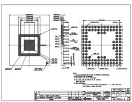
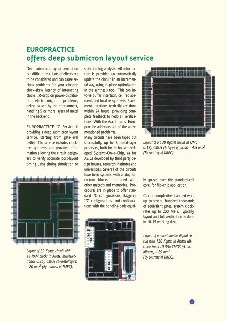
Layout of 29 Kgates circuit with<br />
11 RAM blocks in Alcatel Microelectronics<br />
0.35µ CMOS (5-metallayers)<br />
- 20 mm 2 (By courtesy of IMEC).<br />
static-timing analysis. All information<br />
is provided to automatically<br />
update the circuit in an incremental<br />
way, using in-place optimisation<br />
in the synthesis tool. This can involve<br />
buffer insertion, cell replacement,<br />
and local re-synthesis. Placement-iterations<br />
typically are done<br />
within 24 hours, providing complete<br />
feedback to redo all verifications.<br />
With the Avant! tools, <strong>Europractice</strong><br />
addresses all of the above<br />
mentioned problems.<br />
Many circuits have been taped out<br />
successfully, up to 6 metal-layer<br />
processes, both for in-house developed<br />
Systems-On-a-Chip, as for<br />
ASICs developed by third party design<br />
houses, research institutes and<br />
universities. Several of the circuits<br />
have been systems with analog full<br />
custom blocks, combined with<br />
other macro’s and memories. Procedures<br />
are in place to offer standard<br />
I/O configurations, staggered<br />
I/O configurations, and configurations<br />
with the bonding-pads equal-<br />
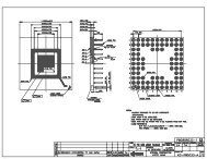
Layout of a 130 Kgates circuit in UMC<br />
0.18µ CMOS (6 layers of metal) - 4.5 mm 2<br />
(By courtesy of IMEC).<br />
ly spread over the standard-cell<br />
core, for flip-chip application.<br />
Circuit complexities handled were<br />
up to several hundred thousands<br />
of equivalent gates, system clockrates<br />
up to 200 MHz. Typically,<br />
layout and full verification is done<br />
in 10-15 working days.<br />
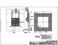
Layout of a mixed analog-digital circuit<br />
with 130 Kgates in Alcatel Microelectronics<br />
0.35µ CMOS (5-metallayers)<br />
- 29 mm 2<br />
(By courtesy of IMEC).<br />
7