X-Ray Photoelectron Spectroscopy (XPS/ESCA) - Philips Research
X-Ray Photoelectron Spectroscopy (XPS/ESCA) - Philips Research
X-Ray Photoelectron Spectroscopy (XPS/ESCA) - Philips Research

You also want an ePaper? Increase the reach of your titles
YUMPU automatically turns print PDFs into web optimized ePapers that Google loves.
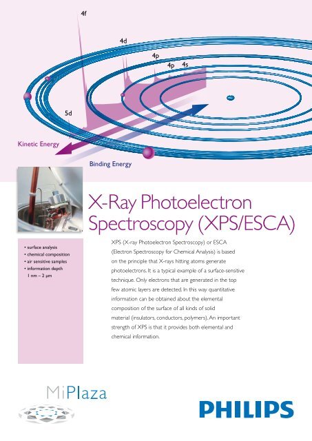
Kinetic Energy<br />
5d<br />
• surface analysis<br />
• chemical composition<br />
• air sensitive samples<br />
• information depth<br />
1 nm – 2 µm<br />
4f<br />
4d<br />
Binding Energy<br />
4p<br />
4p 4s<br />
X-<strong>Ray</strong> <strong>Photoelectron</strong><br />
<strong>Spectroscopy</strong> (<strong>XPS</strong>/<strong>ESCA</strong>)<br />
<strong>XPS</strong> (X-ray <strong>Photoelectron</strong> <strong>Spectroscopy</strong>) or <strong>ESCA</strong><br />
(Electron <strong>Spectroscopy</strong> for Chemical Analysis) is based<br />
on the principle that X-rays hitting atoms generate<br />
photoelectrons. It is a typical example of a surface-sensitive<br />
technique. Only electrons that are generated in the top<br />
few atomic layers are detected. In this way quantitative<br />
information can be obtained about the elemental<br />
composition of the surface of all kinds of solid<br />
material (insulators, conductors, polymers). An important<br />
strength of <strong>XPS</strong> is that it provides both elemental and<br />
chemical information.
CPS<br />
x 104<br />
6<br />
5<br />
4<br />
3<br />
2<br />
1<br />
0<br />
700<br />
Au 4p1<br />
Au 4p3<br />
O 1s<br />
600<br />
Basic principle<br />
Bombarding a sample in vacuum with X-rays<br />
gives rise to the emission of electrons. If<br />
monochromatic X-rays are used with a<br />
photon energy hν, the kinetic energy of the<br />
emitted electrons Ke is given by:<br />
K<br />
e<br />
= hν<br />
− Be<br />
− φ<br />
where Be is the binding energy of the<br />
atomic orbital from which the electron<br />
originates and φ is the work function. The<br />
work function is the minimum amount<br />
of energy an individual electron needs to<br />
escape from the surface.<br />
Each element produces a unique set<br />
of electrons with specific energies. By<br />
measuring the number of these electrons<br />
as a function of kinetic (or binding) energy,<br />
an <strong>XPS</strong> spectrum is obtained. All elements<br />
can be detected, except H and He. Figure 1<br />
shows an example of a survey spectrum of<br />
a SAM layer (self-assembled monolayer) on<br />
gold. <strong>XPS</strong> peaks of C, O, Au, N and S can<br />
be observed.<br />
N 1s<br />
Au 4d3<br />
Au 4d5<br />
C 1s<br />
500 400 300<br />
Binding Energy (eV)<br />
HS NH O<br />
Fig. 2: Molecular structure of biotinylated alkyl thiol (BAT).<br />
O<br />
S 2s<br />
S 2p<br />
200<br />
Au 4f<br />
100<br />
O 2s<br />
Chemical state<br />
Binding energies of photoelectrons depend<br />
on the chemical environment of the atoms.<br />
Accurate measurement of the exact peak<br />
position of the elements present gives<br />
information on the chemical state of these<br />
elements. Figure 3 shows a more detailed<br />
<strong>XPS</strong> spectrum of the sulphur peak of<br />
the SAM layer. A good fit of the signal is<br />
obtained using two double peaks indicating<br />
two different chemical environments of the<br />
sulphur atoms.<br />
Depth profiling<br />
To obtain information at larger depths<br />
(1 – 2 µm at most), concentration profiles<br />
can be recorded by alternating sputtering<br />
with Ar+-ions and spectrum collection.<br />
Typical sputter rates are 5 - 10 nm/min.<br />
A disadvantage of sputtering is that the<br />
chemical state of the elements present<br />
may change due to the ion bombardment.<br />
In addition, the elemental composition may<br />
be influenced by preferential sputtering.<br />
O<br />
O NH<br />
Fig. 3: <strong>XPS</strong> spectrum of S in BAT on gold (see figure 2). Two doublets<br />
(high and low) can be fitted to the signal indicating two different<br />
chemical states of sulphur. The S 2p-low doublet at 161.9 eV<br />
corresponds to the sulphur as Au-thiolate, the S 2p-high doublet at<br />
163.9 eV corresponds to sulphur in the unbound thiophene groups.<br />
O<br />
0<br />
Fig. 1: <strong>XPS</strong> spectrum of a self-assembled monolayer (SAM-layer) of<br />
biotinylated alkyl thiol (see figure 2) on gold. <strong>XPS</strong> peaks of C, N, O, S<br />
and Au, can be observed. The appendix to the element symbol, e.g. 1s<br />
or 2p. denotes the atomic orbital from which the electrons originate.<br />
S<br />
CPS<br />
H<br />
N<br />
226<br />
224<br />
222<br />
220<br />
218<br />
216<br />
214<br />
212<br />
210<br />
208<br />
O<br />
NH<br />
Inert atmosphere<br />
It is also possible to analyze samples that<br />
are sensitive to oxygen, nitrogen and/or<br />
water. These samples can be prepared in<br />
an argon atmosphere and transported to<br />
the <strong>XPS</strong> instrument without exposure to<br />
ambient air.<br />
Micro <strong>XPS</strong><br />
With the aid of a focused X-ray beam it is<br />
possible to obtain data from areas as small<br />
as 10 µm in diameter. Scanning the beam<br />
over the sample allows the acquisition of a<br />
two-dimensional element map as shown in<br />
figure 4. This map makes accurate<br />
positioning of the X-ray beam possible<br />
enabling spatially resolved studies.<br />
S 2p1-high<br />
S 2p3-high<br />
S 2p<br />
S 2p1-low<br />
S 2p3-low<br />
170 168 166 164 162 160 158<br />
Binding Energy (eV)
Quantitative analyses<br />
The number of detected electrons is a<br />
measure for the elemental concentration.<br />
In order to obtain quantitative results, peak<br />
areas are divided by standard sensitivity<br />
factors and normalized to 100% to obtain<br />
atomic concentrations. In this way, for<br />
bulk materials the surface composition can<br />
be determined with a 20% inaccuracy in<br />
concentration. However, most materials<br />
do not have a homogeneous chemical<br />
composition in the upper few nanometers,<br />
but rather a composition that varies as<br />
a function of depth. In the case of a real<br />
multi-layer system the signal of an element<br />
in a lower layer will be attenuated more<br />
strongly than the signal from an element<br />
in the top layer. To obtain quantitative<br />
information for non-homogeneous samples,<br />
either angle-resolved measurements or<br />
model calculations can be performed.<br />
Fig. 5: Schematic of a self-assembled alkane-thiol layer on gold. SAM<br />
layers play an important role in the development of biosensors. The<br />
strong chemical interaction between the thiol (SH) and the gold<br />
surface plus the chain-to-chain interaction of the molecules (e.g. van<br />
der Waals forces) forces the molecules to align parallel to each other<br />
on the gold surface.<br />
S<br />
Au<br />
R<br />
S<br />
R<br />
S<br />
R<br />
S<br />
R<br />
S<br />
Au Au Au Au<br />
Gold Substrate<br />
R<br />
S<br />
Au<br />
Angle-resolved measurements<br />
A way to get more insight into the<br />
composition of a non-homogeneous<br />
sample is to measure a number of spectra<br />
at different measuring angles. Variation of<br />
the emission angle causes changes in the<br />
effective information depth of analysis. At<br />
glancing incidence (small angles) only the<br />
upper layers of the sample are examined;<br />
at high measuring angles deeper layers<br />
are detected. With respect to SAM<br />
layers angle-resolved measurements give<br />
qualitative information about the position<br />
of the sulphur in the layer. In figure 6 ratios<br />
are shown of the relative concentrations<br />
of different elements in a SAM layer,<br />
measured at different angles. The lower the<br />
concentration ratio the deeper the element<br />
is positioned in the sample. Obviously, the<br />
sulphur is closest to the Au substrate<br />
(see figure 5).<br />
R<br />
concentration ratio<br />
4<br />
3.5<br />
3<br />
2.5<br />
2<br />
1.5<br />
1<br />
0.5<br />
0<br />
Fig. 4: At the left a photograph of a pattern of gold<br />
lines in a biosensor is shown. These gold lines are<br />
present at different depths within the device. At<br />
the right the Au X-ray image of the same sensor<br />
is shown. Only the gold line on the upper surface<br />
shows up. This area is covered by a SAM layer.<br />
Model calculation<br />
For the analysis of multilayer systems,<br />
a model calculation method has been<br />
developed. With the model only one<br />
measurement at one measuring angle<br />
is needed to determine thickness and<br />
composition of each layer on the substrate.<br />
SAM layers on gold can be seen<br />
as multilayer systems due to their ordered<br />
structures. For such layers the model gives<br />
insight into the layer composition and allows<br />
the coverage of the gold with sulphur to be<br />
calculated (figure 7).<br />
Fig. 6: Concentrations measured at 25 and 45 degrees divided by the<br />
concentrations measured at 90 degrees for a SAM layer based on CH3 – O -<br />
(CH2 – CH2 – O) 3 – (CH2) 6 – SH on gold. The ratios (especially at 25 degrees)<br />
give a good idea about the position of the different elements in the sample. C<br />
and O are present in the top layer with O at the outer surface. S is closest to<br />
the Au substrate.<br />
20 40 60 80<br />
measuring angle (degrees)<br />
Au<br />
C<br />
O<br />
S
“CO”, O, N, S S-high (thiophene)<br />
“CH 2”<br />
Au substrate<br />
S-low (Au-thiolate)<br />
Remote analysis<br />
The available <strong>XPS</strong>-instruments are part<br />
of the Virtual Laboratory of MiPlaza<br />
Materials Analysis. The Virtual Lab allows<br />
customers to collaborate real-time with the<br />
<strong>XPS</strong>-operator during the analysis of their<br />
samples.<br />
The remote customer only needs a PC with<br />
Internet-browser and obtains access via a<br />
fully protected, encrypted connection. To<br />
setup the connection the remote customer<br />
only needs a session ID; the session ID is<br />
supplied by the operator and is valid for one<br />
session only.<br />
More information to be found at<br />
http://s2s.hightechcampus.nl<br />
©2008 Koninklijke <strong>Philips</strong> Electronics N.V.<br />
All rights reserved.<br />
SAM layer<br />
4.8 nm thick<br />
S coverage: 3.9 10 14 at/cm 2<br />
80 atom % C<br />
9.2 atom % O<br />
7.3 atom % N<br />
1.6 atom % S-low<br />
1.4 atom % S-high<br />
Fig. 7: Multilayer model of BAT on gold (see figure 5). This SAM layer can be seen as two organic layers on top<br />
of the gold substrate: a lower layer containing the –(CH2 ) x – part of the molecules and a top layer containing<br />
predominantly CO groups and N, O and S of the thiophene group. The S of the thiol group is present at the<br />
gold surface only. One single measurement results in the ‘raw’ concentration. A subsequent model calculation<br />
provides the real layer composition, as shown next to the figure.<br />
Applications<br />
• Characterization of thin layers (< 10 nm)<br />
Determination of composition and<br />
effective layer thickness of multilayer<br />
systems (high-k oxide layers on Si, selfassembled<br />
monolayers on a gold substrate,<br />
monolayers of biological materials such as<br />
proteins, antibodies and DNA)<br />
• Characterization of thick layers by<br />
sputtering<br />
Determination of the composition of<br />
layered-structures like ITO-Cr-SiN<br />
systems and of additional (oxide) interface<br />
layers herein<br />
• Contamination<br />
of surfaces of wires, glass, leadframes,<br />
ribbons, inner surface of lamp bulbs<br />
• Effect of specific treatments<br />
like cleaning, heating, oxidation or gas<br />
treatments on the surface composition<br />
• Cause of bad adherence<br />
of e.g. crystals on leadframes, glass-metal<br />
interfaces<br />
• Chemical information<br />
Identification of the chemical state<br />
in which elements are present, i.e.<br />
determination whether a metal is oxidized,<br />
if a salt is present, valence of specific<br />
elements in glasses<br />
MiPlaza Materials Analysis<br />
offers a full range of analytical methods<br />
and expertise to support both research<br />
and manufacturing, serving customers<br />
by taking an integral, solution-oriented<br />
approach.<br />
World-class expertise –<br />
working for you<br />
For more information:<br />
Tel./fax: +31 -40-2748044/42944<br />
E-mail: materials@miplaza.com<br />
www.miplaza.com/materials<br />
Technical Note 3<br />
August 2008<br />
Characteristics<br />
Sample type<br />
• solid materials (bulk, powders,<br />
multi-layers)<br />
Sample sizes<br />
• from a few mm2 up to 70 mm in<br />
diameter; the maximum allowable<br />
thickness of samples is 25 mm<br />
Information depth<br />
• 1 - 10 nm, by sputtering with Ar +-ions<br />
up to approximately 2 µm<br />
Lateral resolution<br />
• ≥ 5 µm for both imaging and<br />
spectroscopy<br />
Detection limit<br />
• 0.01 atom % for heavy elements and<br />
0.1 atom % for light elements<br />
Elemental range<br />
• All elements except H and He