
You also want an ePaper? Increase the reach of your titles
YUMPU automatically turns print PDFs into web optimized ePapers that Google loves.
STR-K880/K900<br />
Ver. 1.1<br />
For Schematic Diagrams.<br />
Note:<br />
• All capacitors are in µF unless otherwise noted. (p: pF)<br />
50 WV or less are not indicated except for electrolytics and<br />
tantalums.<br />
• All resistors are in Ω and 1 /4 W or less unless otherwise<br />
specified.<br />
• % : indicates tolerance.<br />
• f : internal component.<br />
• 2 : nonflammable resistor.<br />
• 5 : fusible resistor.<br />
• C : panel designation.<br />
Note:<br />
The components identified<br />
by mark 0 or dotted<br />
line with mark 0 are<br />
critical for safety.<br />
Replace only with part<br />
number specified.<br />
• A : B+ Line.<br />
• B : B– Line.<br />
• Voltages and waveforms are dc with respect to ground under<br />
no-signal (detuned) conditions.<br />
No mark : FM<br />
• Voltages are taken with a VOM (Input impedance 10 MΩ).<br />
Voltage variations may be noted due to normal production<br />
tolerances.<br />
• Waveforms are taken with a oscilloscope.<br />
• Circled numbers refer to waveforms.<br />
• Signal path.<br />
F : FM<br />
J : ANALOG<br />
c : DIGITAL<br />
I : VIDEO<br />
• Abbreviation<br />
AUS : Australian model.<br />
CND : Canadian model.<br />
E51 : Chilean and Peruvian models.<br />
SP : Singapore model.<br />
SP6 : Singapore and Malaysia models.<br />
14<br />
Note:<br />
Les composants identifiés<br />
par une marque 0 sont critiques<br />
pour la sécurité.<br />
Ne les remplacer que par une<br />
piéce portant le numéro<br />
spécifié.<br />
SECTION 3<br />
DIAGRAMS<br />
THIS NOTE IS COMMON FOR PRINTED WIRING BOARDS AND SCHEMATIC DIAGRAMS.<br />
(In addition to this, the necessary note is printed in each block.)<br />
For Printed Wiring Boards.<br />
Note:<br />
• X : parts extracted from the component side.<br />
• a : Through hole.<br />
• f : internal component.<br />
• : Pattern from the side which enables seeing.<br />
Caution:<br />
Pattern face side: Parts on the pattern face side seen from<br />
(Side B) the pattern face are indicated.<br />
Parts face side: Parts on the parts face side seen from<br />
(Side A) the parts face are indicated.<br />
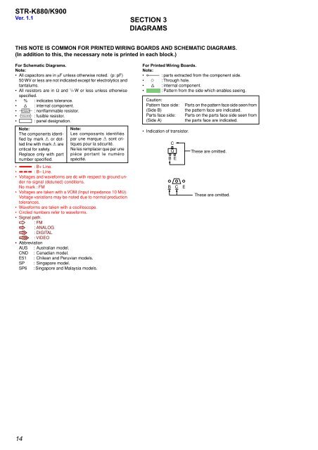
• Indication of transistor.<br />
C<br />
Q<br />
B E<br />
B<br />
C E<br />
These are omitted.<br />
These are omitted.