Near-Infrared Light-Emitting Ambipolar Organic Field-Effect Transistors
Near-Infrared Light-Emitting Ambipolar Organic Field-Effect Transistors
Near-Infrared Light-Emitting Ambipolar Organic Field-Effect Transistors

You also want an ePaper? Increase the reach of your titles
YUMPU automatically turns print PDFs into web optimized ePapers that Google loves.
COMMUNICATION<br />
DOI: 10.1002/adma.200600999<br />
<strong>Near</strong>-<strong>Infrared</strong> <strong>Light</strong>-<strong>Emitting</strong> <strong>Ambipolar</strong> <strong>Organic</strong> <strong>Field</strong>-<strong>Effect</strong><br />
<strong>Transistors</strong>**<br />
By Edsger C. P. Smits, Sepas Setayesh, Thomas D. Anthopoulos, Michael Buechel, Wim Nijssen,<br />
Reinder Coehoorn, Paul W. M. Blom, Bert de Boer, and Dago M. de Leeuw*<br />
Recent years have seen tremendous advances in the area of<br />
organic-based optoelectronic devices and several applications<br />
previously envisioned are now reaching the stage of commercial<br />
exploitation. [1] <strong>Organic</strong> field-effect transistors (OFETs)<br />
are among these devices and can be arguably viewed as a possible<br />
alternative to their inorganic counterparts in a range of<br />
low-cost high-volume applications. [2] Traditionally, OFETs<br />
have been used as pixel switches in active matrix displays and<br />
as the building blocks of integrated circuits where mechanical<br />
flexibility and low-cost fabrication are two prerequisites. [1]<br />
Recently, novel bifunctional OFETs have also made their<br />
debut where, in addition to their classical current-modulating<br />
function, light-emission from within the electroactive channel<br />
has been reported. [3] Such electro-optical transistors are interesting<br />
for two reasons: First, the ability of combining optoelectronic<br />
functionalities in a single device will increase the<br />
number of potential applications, like integrated circuits for<br />
signal-processing that involve both optical and electrical<br />
signals. Secondly, it will provide an ideal experimental platform<br />
for the study of various fundamental physical processes<br />
(optical and electronic) characteristic in organic semiconductors.<br />
– [*] Dr. D. M. de Leeuw, E. C. P. Smits, Dr. S. Setayesh,<br />
Dr. M. Buechel, W. Nijssen, Prof. R. Coehoorn<br />
Philips Research Laboratories<br />
High Tech Campus 4 (WAG 11)<br />
5656 AE Eindhoven (The Netherlands)<br />
E-mail: dago.de.leeuw@philips.com<br />
E. C. P. Smits, Prof. P. W. M. Blom, Dr. B. de Boer<br />
Molecular Electronics, Material Science Centreplus<br />
University of Groningen<br />
Nijenborgh 4, 9747 AG Groningen (The Netherlands)<br />
E. C. P. Smits<br />
Dutch Polymer Institute<br />
Nijenborgh 4, 9747 AG Groningen (The Netherlands)<br />
Dr. T. D. Anthopoulos<br />
Department of Physics, Blackett Laboratory<br />
Imperial College London<br />
London SW7 2BW (UK)<br />
[**] The work of E.C.P.S. forms part of the research program of the<br />
Dutch Polymer Institute (DPI) project No: 516. T.D.A. is grateful to<br />
EC (HPRN-CT-2002-00327) and EPSRC for financial support. T.D.A.<br />
is an EPSRC Advanced Research Fellow. D.M.D.L. and R.C. gratefully<br />
acknowledge the support of the EU projects NAIMO (NMP4-CT-<br />
2004-500355) and RADSAS (NMP3-CT-2004-001561). We are grateful<br />
to Piet Rommers, Inge Vorstenbosch, and Otto Muskens for<br />
their help with performing the CV, PL, and EL measurements and to<br />
Eduard Meijer for his useful discussions.<br />
To date several types of light-emitting OFETs (LEOFETs)<br />
have been demonstrated. The majority of these devices are<br />
“unipolar” in nature (capable of transporting a single chargecarrier<br />
type, i.e., holes or electrons). As a consequence light<br />
emission occurs only at the interface between the semiconductor<br />
and the minority-carrier injecting electrode. [3–8] Only<br />
recently light emission from within the transistor channel was<br />
demonstrated in ambipolar OFETs (i.e., capable of transporting<br />
both holes and electrons). [9–14] In an ambipolar LEOFET<br />
when the gate is biased in between the source and drain<br />
potentials, holes and electrons are injected simultaneously at<br />
the opposite ends of the channel. At the point where the local<br />
potential within the channel equals the gate potential a<br />
pn-junction is formed at which opposite carriers can recombine<br />
to form excitons. When these excitons undergo radiative<br />
decay, the device emits light. The position of the so-called<br />
“recombination zone” can in principle be tuned along the<br />
channel by simply adjusting the gate potential, Vg, and drain<br />
potential, Vd. This has been indeed demonstrated in the<br />
recent works by Zaumseil et al. [12] and Swensen et al. [13] In<br />
both studies, LEOFETs were fabricated using dissimilar<br />
source and drain contact materials to facilitate injection and<br />
transport of both holes and electrons. The use of dissimilar<br />
contacts in combination with suitable gate dielectrics [15] has<br />
been the most suitable method shown so far for fabricating<br />
truly ambipolar LEOFETs.<br />
In this paper, we demonstrate an alternative approach towards<br />
ambipolar LEOFETs based on a solution-processable<br />
small-bandgap squarylium dye. Simultaneous injection of<br />
holes and electrons can be obtained leading to ambipolar<br />
transistor operation because of the low energy gap of the dye<br />
and its favorable position relative to the Fermi level of both<br />
gold source and drain electrodes. Under appropriate bias conditions<br />
holes and electrons recombine within the channel and<br />
the transistor emits light in the near-infrared region of the<br />
electromagnetic spectrum. By invoking an ambipolar-transistor<br />
model we are able to estimate the position of the recombination<br />
zone, at all biasing regimes. Based on these calculations,<br />
the measured change in quantum efficiency as a<br />
function of recombination position within the channel can be<br />
explained. The quantum efficiency of the device is found to<br />
depend only weakly on the position of the recombination<br />
zone along the channel, as long as the recombination zone is<br />
not close to the source or drain contact.<br />
The 2,4-di-3-guaiazulenyl-1,3-dihydroxycyclobutenediyliumdixydroxide-bis<br />
inner salt (SQ1) employed here was pur-<br />
734 © 2007 WILEY-VCH Verlag GmbH & Co. KGaA, Weinheim Adv. Mater. 2007, 19, 734–738
chased from Aldrich Chem. Co. and used directly for device<br />
fabrication without further purification. The molecular structure<br />
of SQ1 is shown in the inset of Figure 1. The material<br />
was found to be highly soluble in a variety of common organic<br />
solvents. The UV-vis absorption spectrum in the solid-state<br />
Figure 1. UV-vis absorption, photoluminescence (PL), and electroluminescence<br />
(EL) spectra for an SQ1 film. The inset shows the molecular<br />
structure of SQ1.<br />
(thin film) is shown in Figure 1. A single peak at approximately<br />
911 nm is observed. From the absorption onset of the<br />
spectrum, the energy gap between the highest molecular<br />
orbital (HOMO) and lowest unoccupied molecular orbital<br />
(LUMO) is calculated to be 1–1.2 eV. In the solid state, the<br />
HOMO–LUMO gap was determined using an electrochemical<br />
technique with the dye deposited on a glassy carbon electrode<br />
employing dichloromethane as the solvent. From the<br />
onset of the redox peaks a bandgap of ca. 1.2 eV was determined<br />
with HOMO and LUMO levels respectively at –5.0 eV<br />
and –3.8 eV with respect to the vacuum level. Photoluminescence<br />
(PL) measurements were also performed on annealed<br />
films of SQ1 using a 633 nm excitation wavelength from a<br />
diode laser. The obtained spectrum is shown in Figure 1<br />
where a narrow emission peak can be observed at 945 nm.<br />
Radiative recombination was confirmed by using electroluminescence<br />
(EL) measurements. The EL spectrum obtained for<br />
an ITO/SQ1/Ba(Al) diode was similar to the PL spectrum, as<br />
shown in Figure 1.<br />
Bottom-contact field-effect transistors were fabricated by<br />
solution-processing SQ1 on the top of prepatterned substrates.<br />
[16] Details of the fabrication process are given in the<br />
Experimental section. Figure 2a (symbols) shows the ambipolar<br />
transfer characteristics of a SQ1-based transistor at different<br />
biasing regimes. The solid lines represent the simulated<br />
curves using the ambipolar transport model discussed later. [16]<br />
The maximum hole and electron mobilities derived from the<br />
transfer curves of Figure 2a are approximately equal and in<br />
the order of 10 –4 cm 2 V – s –1 . We note, however, that mobility<br />
values were strongly dependent on the film morphology because<br />
of the crystallization occurring upon annealing, which<br />
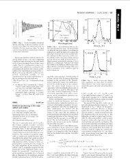
(a)<br />
(b)<br />
(c)<br />
Figure 2. a) Transfer characteristics of an ambipolar transistor (channel<br />
length L= 2.5 lm, and width W = 50 cm) based on SQ1 at different biasing<br />
regimes. Symbols represent the experimental results and solid lines<br />
the theoretical fits using the ambipolar model as described by Smits<br />
et al. [16] The fitting parameters employed are summarized in the text.<br />
The inset shows the schematic of the bottom-contact transistor architecture<br />
employed. b) The light intensity measured with a photodiode (Ip)<br />
positioned above the transistor as a function of drain and gate biases.<br />
c) The ratio of the measured photodiode current over drain current (I p/I ds)<br />
versus gate bias (V g) at different drain voltages. The shadowed area<br />
represents the estimated error caused by the photodiodes dark current.<br />
led to a significant parameter spread between samples. For our<br />
best transistors hole mobilities as high as 1 × 10 –3 cm 2 V – s –1<br />
were measured.<br />
Under appropriate bias conditions we observed infraredlight<br />
emission from within the electroactive transistor channel.<br />
Figure 2b shows the photodiode current (Ip) as a function<br />
of positive and negative Vg and Vd voltages. For each biasing<br />
Adv. Mater. 2007, 19, 734–738 © 2007 WILEY-VCH Verlag GmbH & Co. KGaA, Weinheim www.advmat.de 735<br />
COMMUNICATION
COMMUNICATION<br />
regime the photodiode current showed two maxima, the position<br />
of which depended on the Vd voltage. We observed that<br />
when the source–drain current is at a minimum, which was<br />
the case when V g – V t ≈ V d/2 for similar hole and electron mobilities,<br />
the photodiode current was also at a minimum. This<br />
was, however, the position where the recombination was calculated<br />
to be located in the middle of the channel. As Ip is<br />
proportional to the number of emitted photons from within<br />
the channel of the ambipolar OFET, and the source–drain<br />
current (Ids) is expected to be proportional to the number of<br />
injected carriers (holes and electrons), we plotted the ratio of<br />
I p/I ds (∝ external quantum efficiency) versus V g at different<br />
Vd voltages. These results are displayed in Figure 2c. The<br />
shadowed areas represent the error margins for each<br />
measured point, which were introduced by the dark current<br />
in the photodiode (0.1–0.5 pA). This dark current, although<br />
very low, was comparable to Ids for Vg, where Ids was at a<br />
minimum (see Fig. 2a) and responsible for the I p/I ds uncertainty<br />
in this V g region. Overall, a slight increase in I p/I ds with<br />
increasing current was observed, the origin of which is not<br />
understood at present. It is evident from this figure that the<br />
trace resembles a single broad peak/plateau with a small substructure<br />
(at each biasing regime). These are in agreement<br />
with results previously published. [12] This broad peak emission<br />
occurs when the device is operated in a pn-junction regime<br />
(⏐V d⏐ > ⏐V g – V t⏐ > 0, where V t is the threshold voltage).<br />
The reduction of emitted light at higher and lower V g has<br />
also been observed previously for LEOFETs driven in constant-current<br />
mode. Zaumseil et al. [12] have argued that there<br />
are two possible mechanisms responsible for this observation:<br />
one is the metal-induced EL quenching occurring near the<br />
metal electrodes, and the second is the direct transport of<br />
electrons and/or holes to the metal electrode without recombining.<br />
For the latter mechanism to occur, the recombination<br />
zone has to be in very close proximity to the metal electrode,<br />
which would mean that the transistor would start to operate<br />
in unipolar mode. To elucidate the origin of this effect in our<br />
devices we employed a microscopic transport model developed<br />
recently for ambipolar organic transistors. [16] This model<br />
is based on the variable-range hopping theory in an exponential<br />
density of states (DOS) [17] and has been shown to give a<br />
fair description of OFETs based on disordered semiconductors.<br />
[18] We assume that in the ambipolar transistor complete<br />
charge recombination occurs in a planar zone perpendicular<br />
to the channel, with a width that is much smaller than the<br />
source–drain distance. Under these circumstances we may approximate<br />
the device to consist of two spatially separated<br />
transistors, an n-type and a p-type, connected in series. The<br />
length of each transistor (L e for electrons and L h for holes<br />
with L= L e + L h) depends on the drain and gate voltages. This<br />
implies that at each electrode the current is carried only by<br />
one type of charge carrier, hence the current in the electron<br />
channel can be written as<br />
I ds;e…x < x 0†ˆ W<br />
x 0<br />
T<br />
ce 2T0;e T<br />
2T 0;e T V g V t<br />
2T 0;e<br />
T …1†<br />
with<br />
c e ˆ r 0;e<br />
q<br />
0<br />
B<br />
@<br />
×<br />
T 0;e<br />
T<br />
4<br />
sin p T<br />
T 0;e<br />
… 2ae† 3 BC 1<br />
2kBT0;eeSe0 1<br />
C<br />
A<br />
T0;e T<br />
T0;e T<br />
1<br />
C<br />
2T0;e T<br />
and the hole current can be expressed as<br />
I ds;h…x 0 < x < L† ˆ<br />
with<br />
c h ˆ r 0;h<br />
q<br />
W<br />
L x0 0<br />
B<br />
@<br />
×<br />
T<br />
ch 2T0;h T 0;h<br />
T<br />
T<br />
2T 0;h T V d V g ‡ V t<br />
4<br />
sin p T<br />
T 0;h<br />
… 2ah† 3 BC 1<br />
2kBT0;heSe0 1<br />
C<br />
A<br />
T0;h T<br />
T0;h T<br />
1<br />
C<br />
i<br />
2T0;h T<br />
i<br />
1<br />
1<br />
…2†<br />
2T 0;h<br />
T …3†<br />
where x is the position in channel parallel to the source drain,<br />
x0 the position in the channel of recombination plane, W and<br />
L are the width and channel length of the transistor, respectively,<br />
T is the temperature, T 0,e and T 0,h are the characteristic<br />
temperatures that indicate the widths of the exponential DOS<br />
for the electrons and holes, respectively, Vt is the threshold<br />
voltage, [16,17] q is the elementary charge, kB is the Boltzmann<br />
constant, BC is a critical number for the onset of percolation<br />
(= 2.8 for a 3D amorphous system [17] ), Ci is the geometric<br />
capacitance of the gate dielectric per unit area (17 nF cm –2 ), e 0<br />
is the relative permittivity of a vacuum, e s (ca. 3) is the dielectric<br />
constant of the semiconductor, r 0,e and r 0,h are the conductivity<br />
pre-factors for the electrons and holes respectively,<br />
and finally ah –1 and ae –1 are the wave-function localization<br />
length for the holes and electrons, respectively.<br />
From the condition of current conservation (Ids,e(x < x0)=<br />
Ids,h(x0 < x)), the following expression for the position of the<br />
recombination zone within the channel, x 0, can be derived<br />
x0 ˆ<br />
A Vd where<br />
A ˆ 2T 0;e<br />
2T 0;h<br />
V g<br />
V g ‡ V t<br />
T<br />
T<br />
T0;e ch T0; h ce V t<br />
2T 0;h<br />
2T0;e T<br />
T ‡ V g V t<br />
2T0;e T<br />
…4†<br />
L …5†<br />
736 www.advmat.de © 2007 WILEY-VCH Verlag GmbH & Co. KGaA, Weinheim Adv. Mater. 2007, 19, 734–738<br />
…6†
Finally, substituting Equation 5 for x0 into Equation 1 yields:<br />
Ids ˆ W<br />
L ce T<br />
2T 0;e<br />
T<br />
‡ch 2T0;h T<br />
2T 0;e T V g V t<br />
2T0;e T<br />
T<br />
2T 0;h T V d V g ‡ V t<br />
2T 0;h<br />
T † …7†<br />
Using Equation 7 we were able to fit the experimental curves<br />
of Figure 2a (symbols) employing two set of parameters, one<br />
for the holes and one for the electrons. From the fits, the characteristic<br />
temperature of the width of the exponential DOS<br />
for both carriers was obtained yielding T 0,h = 585 K and<br />
T0,e = 514 K. Furthermore, we obtained ch = 2.0 × 10 –15 and<br />
ce = 1.0 × 10 –14 . The values of a –1 and r0 for holes and electrons<br />
can be determined from temperature-dependent measurements.<br />
However, that is out of the scope of this Communication.<br />
Vt, was found to be –2 V for a measurement sweep going<br />
from negative to positive gate bias (positive V d) and 2 V for a<br />
sweep going from a positive to a negative gate bias (negative<br />
Vd). The observed shift in Vt was attributed to electrical stressing<br />
of the device, a well-documented process. [19] The parameter<br />
values T0 and c obtained for SQ1 are comparable with<br />
values reported in the literature for several other organic<br />
semiconductors. [16,18] Theoretical curves are represented as<br />
the solid lines in Figure 2a. From this figure it is evident that<br />
for V g – V t biases close to V d/2, a discrepancy between measured<br />
and simulated data was observed. We attribute this to<br />
parasitic contact effects, [20,21] which were not taken into account<br />
in the model. Despite this discrepancy, however, a good<br />
description of the experimental data can be obtained in both<br />
operating regimes, that is, in hole and electron accumulation.<br />
By substituting the fit parameters into Equation 5 we were<br />
able to calculate the position of the recombination zone as a<br />
function of V g at positive V d voltages. This plot is shown in<br />
Figure 3a. As can be seen, the recombination zone could be<br />
shifted throughout the channel by tuning the Vg and Vd potential,<br />
in agreement with previous experimental observations.<br />
[12,13] In order to study the effects of the position of the<br />
recombination zone along the channel on Ip/Ids, we have combined<br />
the experimental data of Figure 2b with the theoretical<br />
predictions of Equation 5. The resulting plot is shown in Figure<br />
3b, where I p/I ds is plotted versus the calculated position of<br />
the recombination zone. From this analysis we found that near<br />
the metal contacts a drastic lowering of Ip/Ids occurred. At distances<br />
beyond a few hundred nanometers from the contacts,<br />
the external efficiency of the device was only weakly dependent<br />
on the position of the recombination zone along the<br />
channel, if one takes the experimental error (shadowed area)<br />
introduced by the dark current in the photodiode current into<br />
account. This observation is consistent with the assumption<br />
that full recombination takes place in a relatively narrow<br />
zone, and provides, thus, further experimental evidence for<br />
the validity of the model. From studies performed on organic<br />
light-emitting diodes (OLEDs) it is known that the distance<br />
(a)<br />
(b)<br />
Figure 3. a) The calculated position (source to drain) of the recombination<br />
zone (using Eq. 4) versus Vg at different Vd (DVd = 5 V). b) Measured<br />
Ip/Ids versus calculated position of the recombination zone at different<br />
Vd. Shadowed areas represent the estimated error caused by the<br />
photodiodes dark current. The grayed areas represent the position of the<br />
source and drain electrodes in space.<br />
of around a hundred nanometers is too large for metalinduced<br />
EL quenching to occur. [22] However, a direct comparison<br />
between OLEDs and LEOFETs would be inappropriate<br />
because of the different device geometry. Another possible<br />
explanation for the decay of I p/I ds near the contacts would be<br />
that the recombination zone itself has a width of the order of<br />
a hundred nanometers. Such a zone would still be narrow<br />
compared to the channel length so that the basic assumption<br />
that led to Equation 5 would still remain valid. [16]<br />
In summary, operation of a near-infrared light-emitting<br />
ambipolar organic transistor has been demonstrated. The advantage<br />
of this device is twofold: i) it employs similar source<br />
and drain contacts of gold, and ii) it relies on a single, solution-processable<br />
organic semiconductor. Such a device configuration,<br />
in combination with the theoretical model presented<br />
here, provides a powerful tool towards a better understanding<br />
of the various electronic processes within organic materials<br />
under different conditions.<br />
Experimental<br />
Device Fabrication: <strong>Ambipolar</strong> field-effect transistors were fabricated<br />
using heavily doped p-type Si wafers as the common gate elec-<br />
Adv. Mater. 2007, 19, 734–738 © 2007 WILEY-VCH Verlag GmbH & Co. KGaA, Weinheim www.advmat.de 737<br />
COMMUNICATION
COMMUNICATION<br />
trode with a 200 nm thermally oxidized SiO2 layer as the gate dielectric.<br />
Using conventional photolithography, gold source and drain electrodes<br />
were defined in a bottom contact device configuration (Fig. 2a,<br />
inset) with channel width (W) and length (L) of 50 cm and 2.5 lm, respectively.<br />
A 10 nm layer of Ti was used, acting as an adhesion layer<br />
for the Au on SiO2. The SiO2 layer was treated with the primer hexamethyldisilazane<br />
prior to semiconductor deposition in order to passivate<br />
its surface. Films were spun from a 10 mg mL –1 solution of SQ1<br />
in chloroform at 800 rpm for half a minute. Freshly prepared devices<br />
were annealed in vacuum of 10 –6 mbar (1 bar = 100 000 Pa) at 115 °C<br />
for one hour. All electrical and optical measurements were performed<br />
in high vacuum (10 –6 mbar) at room temperature using an HP 4155C<br />
semiconductor parameter analyzer. <strong>Light</strong> emission was measured<br />
using a Si pin-diode (Siemens BPX61) placed in close proximity<br />
above the transistors.<br />
Absorption, Electroluminescence, and Photoluminescence Measurements:<br />
For UV-vis absorption measurements SQ1 was spin-coated on<br />
a glass substrate from a chloroform solution and subsequently annealed<br />
at 115 °C. The absorption spectrum was recorded with a Perkin<br />
Elmer Labda 950 spectrometer. PL measurements on SQ1 films were<br />
performed on the same sample used for the transistor devices fabricated<br />
side by side. The film was excited with a 633 nm HeNe laser and<br />
the PL spectrum was recorder using a Horiba Jobin Yvon Labram<br />
spectrograph equipped with a deep-depletion nitrogen-cooled CCD<br />
camera (400–1050 nm). The EL spectrum from the diode structures<br />
was measured with an Andor Shamrock SR 303i-A spectrometer<br />
equipped with an Andor Idus CCD camera. Cyclic-voltammogram<br />
(CV) measurements were performed using a 757 VA Computrace system<br />
from Metrohm. The CVs were recorded under an Ar atmosphere<br />
in acetonitride/Tetrabutylammoniumhexafluorophosphate on a glassy<br />
carbon working electrode. The redox potential was calibrated against<br />
the internal reference Fc/Fc + couple.<br />
Received: May 8, 2006<br />
Revised: November 6, 2006<br />
Published online: January 25, 2007<br />
–<br />
[1] G. H. Gelinck, H. E. A. Huitema, E. Van Veenendaal, E. Cantatore,<br />
L. Schrijnemakers, J. B. P. H. van der Putten, T. C. T. Geuns,<br />
M. Beenhakkers, J. B. Giesbers, B. Huisman, E. J. Meijer, E. Mena<br />
Benito, F. J. Touwslager, A. W. Marsman, B. J. E. van Rens, D. M.<br />
de Leeuw, Nat. Mater. 2004, 3, 106.<br />
[2] A. Knobloch, A. Manuelli, A. Bernds, W. Clemens, J. Appl. Phys.<br />
2004, 96, 2286.<br />
______________________<br />
[3] A. Hepp, H. Heil, W. Weise, M. Ahles, R. Schmechel, H. von Seggern,<br />
Phys. Rev. Lett. 2003, 91, 157 406.<br />
[4] C. Santato, R. Capelli, M. A. Loi, M. Murgia, F. Cicoira, V. A. L.<br />
Roy, P. Stallinga, R. Zamboni, C. Rost, S. F. Karg, M. Muccini,<br />
Synth. Met. 2004, 146, 329.<br />
[5] T. Oyamada, H. Sasabe, C. Adachi, S. Okuyama, N. Shimoji, K. Matsushige,<br />
Appl. Phys. Lett. 2005, 86, 93 505.<br />
[6] C. Santato, I. Manunza, A. Bonfiglio, F. Cicoira, P. Cosseddu,<br />
R. Zamboni, M. Muccini, Appl. Phys. Lett. 2005, 86, 141 106.<br />
[7] F. Cicoira, C. Santato, M. Melucci, L. Favaretto, M. Gazzano,<br />
M. Muccini, G. Barbarella, Adv. Mater. 2006, 18, 169.<br />
[8] M. Ahles, A. Hepp, R. Schmechel, H. Von Seggern, Appl. Phys. Lett.<br />
2004, 84, 428.<br />
[9] C. Rost, S. Karg, W. Riess, M. A. Loi, M. Murgia, M. Muccini, Synth.<br />
Met. 2004, 146, 237.<br />
[10] C. Rost, S. Karg, W. Riess, M. A. Loi, M. Murgia, M. Muccini, Appl.<br />
Phys. Lett. 2004, 85, 1613.<br />
[11] J. Reynaert, D. Cheyns, D. Janssen, R. Muller, V. I. Arkhipov,<br />
J. Genoe, G. Borghs, P. Heremans, J. Appl. Phys. 2005, 97, 114 501.<br />
[12] J. Zaumzeil, R. H. Friend, H. Sirringhaus, Nat. Mater. 2006, 5, 69.<br />
[13] J. S. Swensen, C. Soci, A. J. Heeger, Appl. Phys. Lett. 2005, 87,<br />
253 511.<br />
[14] M. A. Loi, C. Rost-Bietsch, M. Murgia, S. Karg, W. Riess, M. Muccini,<br />
Adv. Funct. Mater. 2006, 16, 41.<br />
[15] L. Chua, J. Zaumseil, J. Chang, E. C.-W. Ou, P. K.-H. Ho, H. Serringhaus,<br />
R. H. Friend, Nature 2005, 434, 194.<br />
[16] E. C. P. Smits, T. D. Anthopoulos, S. Setayesh, E. van Veenendaal,<br />
R. Coehoorn, P. W. M. Blom, B. de Boer, D. M. de Leeuw, Phys.<br />
Rev. B: Condens. Matter 2006, 73, 205 316.<br />
[17] M. C. J. M. Vissenberg, M. Matters, Phys. Rev. B: Condens. Matter<br />
1998, 57, 12 964.<br />
[18] E. J. Meijer, C. Tanase, P. W. M. Blom, E. van Veenendaal, B.-H.<br />
Huisman, D. M. de Leeuw, T. M. Klapwijk, Appl. Phys. Lett. 2002,<br />
80, 3838.<br />
[19] A. Salleo, R. A. Street, J. Appl. Phys. 2003, 94, 471.<br />
[20] T. D. Anthopoulos, D. M. de Leeuw, E. Cantatore, S. Setayesh, E. J.<br />
Meijer, C. Tanase, J. C. Hummelen, P. W. M. Blom, Appl. Phys. Lett.<br />
2004, 85, 4205.<br />
[21] T. D. Anthopoulos, C. Tanase, S. Setayesh, E. J. Meijer, J. C. Hummelen,<br />
P. W. M. Blom, D. M. Leeuw. Adv. Mater. 2004, 16, 2174.<br />
[22] a) D. E. Markov, P. W. M. Blom, Appl. Phys. Lett. 2005, 87, 233 511.<br />
b) D. E. Markov, P. W. M. Blom, Phys. Rev. B: Condens. Matter<br />
2005, 72, 161 401.<br />
738 www.advmat.de © 2007 WILEY-VCH Verlag GmbH & Co. KGaA, Weinheim Adv. Mater. 2007, 19, 734–738