UWB-MIMO ANTENNA WITH NOVEL STUB STRUCTURE A ... - PIER
UWB-MIMO ANTENNA WITH NOVEL STUB STRUCTURE A ... - PIER
UWB-MIMO ANTENNA WITH NOVEL STUB STRUCTURE A ... - PIER

Create successful ePaper yourself
Turn your PDF publications into a flip-book with our unique Google optimized e-Paper software.
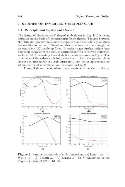
248 Najam, Duroc, and Tedjni<br />
3. STUDIES ON INVERTED-Y SHAPED <strong>STUB</strong><br />
3.1. Principle and Equivalent Circuit<br />
The design of the inverted-Y shaped stub shown in Fig. 1(b) is being<br />
initiated on the basis of the microstrip filters theory. The gap between<br />
the stub and ground plane acts as capacitor and the side legs of stubs<br />
behave like inductors. Therefore, this structure can be thought of<br />
an equivalent LC bandstop filter. In order to get further insight into<br />
bandstop behavior of the stub, it is printed on FR4 substrate connected<br />
with two 50 Ω microstrip lines at its both ends as shown in Fig. 2. The<br />
other side of the substrate is fully metalized to form the ground plane<br />
except the area under the stub structure to get better approximation<br />
where the metal is scratched out as shown in Fig. 2.<br />
Figure 3 shows the simulated S-parameters of the stub. Initially,<br />
(a) (b)<br />
(c)<br />
Figure 2. Parametric analysis of stub dimensions. (a) Length L5. (b)<br />
Width W3. (c) Length L6. (d) Length L7, for S-parameters in the<br />
frequency range of 3.2–10.6 GHz.<br />
(d)