Application Compendium - Agilent Technologies
Application Compendium - Agilent Technologies
Application Compendium - Agilent Technologies

You also want an ePaper? Increase the reach of your titles
YUMPU automatically turns print PDFs into web optimized ePapers that Google loves.
A<br />
B<br />
C<br />
D<br />
Abs. at 3692 cm -1<br />
Abs. Range 1180-1060 cm -1<br />
Abs. at 3265 cm -1<br />
Abs. at 1370 cm -1<br />
Layer 1<br />
Layer 2<br />
Layer 3<br />
Layer 4<br />
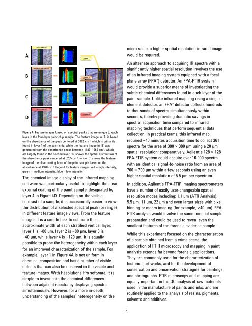
Figure 4. Feature images based on spectral peaks that are unique to each<br />
layer in the four-layer paint chip sample. The feature image in „A‟ is based<br />
on the absorbance of the peak centered at 3692 cm -1 , which is primarily<br />
found in layer 1 of the paint chip; while the feature image in „B‟ was<br />
generated from the absorbance peaks between 1180–1060 cm -1 , which<br />
are largely found in the second layer; „C‟ shows the spatial distribution of<br />
the absorbance peak centered at 3265 cm -1 ; while „D‟ shows the feature<br />
image of the clear coating layer of the paint sample based on the<br />
absorbance at 1370 cm -1 . Legend for feature images: red = high intensity,<br />
green = medium intensity, blue = low intensity.<br />
The chemical image display of the infrared mapping<br />
software was particularly useful to highlight the clear<br />
external coating of the paint sample, designated by<br />
layer 4 in Figure 4D. Depending on the visible<br />
contrast of a sample, it is occasionally easier to view<br />
the distribution of a selected spectral peak (or range)<br />
in different feature image views. From the feature<br />
images it is a simple task to estimate the<br />
approximate width of each stratified vertical layer;<br />
layer 1 is ~80 µm, layer 2 is ~80 µm, layer 3 is<br />
~40 µm, while layer 4 is ~120 µm. It is equally<br />
possible to probe the heterogeneity within each layer<br />
for an improved characterization of the sample. For<br />
example, layer 1 in Figure 4A is not uniform in<br />
chemical composition and has a number of visible<br />
defects that can also be observed in the visible and<br />
feature images. With Resolutions Pro software, it is<br />
simple to investigate the chemical differences<br />
between adjacent spectra by displaying spectra<br />
simultaneously. However, for a more in-depth<br />
understanding of the samples‟ heterogeneity on the<br />
micro-scale, a higher spatial resolution infrared image<br />
would be required.<br />
An alternate approach to acquiring IR spectra with a<br />
significantly higher spatial resolution involves the use<br />
of an infrared imaging system equipped with a focal<br />
plane array (FPA*) detector. An FPA-FTIR system<br />
would provide a superior means of investigating the<br />
subtle chemical differences found in each layer of the<br />
paint sample. Unlike infrared mapping using a singleelement<br />
detector, an FPA* detector collects hundreds<br />
to thousands of spectra simultaneously within<br />
seconds, thereby providing dramatic savings in<br />
spectral acquisition time compared to infrared<br />
mapping techniques that perform sequential data<br />
collection. In practical terms, this infrared map<br />
required ~40 minutes acquisition time to collect 361<br />
spectra for the area of 380 × 380 µm using a 20 µm<br />
spatial resolution; comparatively, <strong>Agilent</strong>‟s 128 × 128<br />
FPA-FTIR system could acquire over 16,000 spectra<br />
with an identical signal-to-noise ratio from an area of<br />
700 × 700 µm within a few seconds using an even<br />
higher spatial resolution of 5.5 µm per spectrum.<br />
In addition, <strong>Agilent</strong>‟s FPA-FTIR imaging spectrometers<br />
have a number of easily user-changeable spatial<br />
resolution modes including: 1.1 µm (ATR Analysis),<br />
5.5 µm, 11 µm, 22 µm and even larger sizes with pixel<br />
binning or macro imaging (for example, >40 µm). FPA-<br />
FTIR analysis would involve the same minimal sample<br />
preparation and could be used to reveal even the<br />
smallest features of the forensic evidence sample.<br />
While this experiment focused on the characterization<br />
of a sample obtained from a crime scene, the<br />
application of FTIR microscopy and mapping in paint<br />
analysis extends far beyond forensic applications.<br />
They are commonly used for the characterization of<br />
historical art works, and for the development of<br />
conservation and preservation strategies for paintings<br />
and photographs. FTIR microscopy and mapping are<br />
equally important in the QC analysis of raw materials<br />
used in the manufacture of paints and inks, and are<br />
routinely applied to the analysis of resins, pigments,<br />
solvents and additives.<br />
5