AR-B1047 SOLID STATE DISK CARD User¡¦s Guide - Acrosser
AR-B1047 SOLID STATE DISK CARD User¡¦s Guide - Acrosser
AR-B1047 SOLID STATE DISK CARD User¡¦s Guide - Acrosser

Create successful ePaper yourself
Turn your PDF publications into a flip-book with our unique Google optimized e-Paper software.
<strong>AR</strong>-<strong>B1047</strong><br />
<strong>SOLID</strong> <strong>STATE</strong> <strong>DISK</strong> C<strong>AR</strong>D<br />
User¡ƒs <strong>Guide</strong><br />
Edition: 1.4<br />
Book Number: <strong>AR</strong>-<strong>B1047</strong>-98.A04
Table of Contents<br />
<strong>AR</strong>-<strong>B1047</strong> User¡ƒs <strong>Guide</strong><br />
0. PREFACE....................................................................................................................................................... 0-2<br />
0.1 COPYRIGHT NOTICE AND DISCLAIMER ................................................................................................................................0-2<br />
0.2 WELCOME TO THE <strong>AR</strong>-<strong>B1047</strong> ROM C<strong>AR</strong>D.............................................................................................................................0-2<br />
0.3 BEFORE YOU USE THIS GUIDE...............................................................................................................................................0-2<br />
0.4 RETURNING YOUR BO<strong>AR</strong>D FOR SERVICE............................................................................................................................0-2<br />
0.5 TECHNICAL SUPPORT AND USER COMMENTS...................................................................................................................0-2<br />
0.6 ORGANIZATION..........................................................................................................................................................................0-3<br />
0.7 STATIC ELECTRICITY PRECAUTIONS....................................................................................................................................0-3<br />
1. OVERVIEW..................................................................................................................................................... 1-1<br />
1.1 INTRODUCTION .........................................................................................................................................................................1-1<br />
1.2 PACKING LIST ............................................................................................................................................................................1-2<br />
1.3 FEATURES..................................................................................................................................................................................1-2<br />
2. SETTING UP THE SYSTEM............................................................................................................................ 2-1<br />
2.1 OVERVIEW..................................................................................................................................................................................2-1<br />
2.2 SYSTEM SETTING .....................................................................................................................................................................2-2<br />
2.2.1 Battery Setting .....................................................................................................................................................................2-2<br />
2.2.2 PC/104 Connector...............................................................................................................................................................2-3<br />
2.3 DIP SWITCH SETTING (SW1) ...................................................................................................................................................2-4<br />
2.3.1 I/O Port Address Select (SW1-1)........................................................................................................................................2-4<br />
2.3.2 SSD & DiskOnChip Firmware Address Select (SW1-2, SW1-7 & SW1-8)...................................................................................2-4<br />
2.3.3 SSD Drive Number (SW1-3 & SW1-4) ...............................................................................................................................2-5<br />
2.3.4 ROM Type Select (SW1-5 & SW1-6)..................................................................................................................................2-6<br />
2.4 MEMORY TYPE SETTING (M1, M2 & M3)................................................................................................................................2-7<br />
3. INSTALLATION .............................................................................................................................................. 3-1<br />
3.1 OVERVIEW..................................................................................................................................................................................3-1<br />
3.2 ROM <strong>DISK</strong> INSTALLATION........................................................................................................................................................3-1<br />
3.2.1 UV EPROM (27Cxxx)..........................................................................................................................................................3-5<br />
3.2.2 12V or Large Page 5V FLASH Disk....................................................................................................................................3-6<br />
3.2.3 Small Page 5V FLASH ROM Disk......................................................................................................................................3-8<br />
3.2.4 RAM Disk.............................................................................................................................................................................3-9<br />
3.2.5 Combination of ROM and RAM Disk ................................................................................................................................3-10<br />
3.3 USING THE WRITE PROTECT FUNCTION............................................................................................................................3-11<br />
3.4 MEMORY DEVICE SUPPORTED ............................................................................................................................................3-12<br />
3.5 HOW TO USE THE D.O.C. .......................................................................................................................................................3-12<br />
4. HOW TO USE THE MEMORY BANKS ................................................................................................................... 4-1<br />
5. SPECIFICATIONS & SSD TYPE SUPPORTED ............................................................................................... 5-1<br />
5.1 SPECIFICATIONS.......................................................................................................................................................................5-1<br />
5.2 SSD TYPE SUPPORTED ...........................................................................................................................................................5-1<br />
6. PLACEMENT & DIMENSIONS........................................................................................................................ 6-1<br />
6.1 PLACEMENT ...............................................................................................................................................................................6-1<br />
6.2 DIMENSIONS ..............................................................................................................................................................................6-2<br />
7. INDEX............................................................................................................................................................. 7-1<br />
0-1
<strong>AR</strong>-<strong>B1047</strong> User¡ƒs <strong>Guide</strong><br />
0.1 COPYRIGHT NOTICE AND DISCLAIMER<br />
0-2<br />
0. PREFACE<br />
August 1998<br />
<strong>Acrosser</strong> Technology makes no representations or warranties with respect to the contents hereof and specifically<br />
disclaims any implied warranties of merchantability or fitness for any particular purpose. Furthermore, <strong>Acrosser</strong><br />
Technology reserves the right to revise this publication and to make changes from time to time in the contents<br />
hereof without obligation of <strong>Acrosser</strong> Technology to notify any person of such revisions or changes.<br />
Possession, use, or copying of the software described in this publication is authorized only pursuant to a valid<br />
written license from <strong>Acrosser</strong> or an authorized sublicensor.<br />
(C) Copyright <strong>Acrosser</strong> Technology Co., Ltd., 1998. All rights Reserved.<br />
No part of this publication may be reproduced, transmitted, transcribed, stored in a retrieval system, or translated<br />
into any language or computer language, in any form or any means, electronic, mechanical, magnetic, optical,<br />
chemical, manual or otherwise, without the prior written consent of <strong>Acrosser</strong> Technology.<br />
<strong>Acrosser</strong>, IBM PC/AT, MS-DOS, PC-DOS, DR-DOS, X-DOS, …are registered trademarks.<br />
All other trademarks and registered trademarks are the property of their respective holders.<br />
This document was produced with Adobe Acrobat 3.01.<br />
0.2 WELCOME TO THE <strong>AR</strong>-<strong>B1047</strong> ROM C<strong>AR</strong>D<br />
This guide introduces the <strong>Acrosser</strong> <strong>AR</strong>-<strong>B1047</strong> ROM Card.<br />
Use the information describes this card’ s functions, features, and how to start, set up and operate your <strong>AR</strong>-<br />
<strong>B1047</strong>. You also could find general system information here.<br />
0.3 BEFORE YOU USE THIS GUIDE<br />
If you have not already installed this <strong>AR</strong>-<strong>B1047</strong>, refer to the Chapter 2, “ Setting Up the System” in this guide.<br />
Check the packing list, make sure the accessories in the package.<br />
The <strong>AR</strong>-<strong>B1047</strong> diskette provides the newest information about the card. Please refer to the README.DOC file<br />
of the enclosed utility diskette. It contains the modification and hardware & software information, and adding<br />
the description or modification of product function after manual published.<br />
0.4 RETURNING YOUR BO<strong>AR</strong>D FOR SERVICE<br />
If your board requires servicing, contact the dealer from whom you purchased the product for service information.<br />
If you need to ship your board to us for service, be sure it is packed in a protective carton. We recommend that<br />
you keep the original shipping container for this purpose.<br />
You can help assure efficient servicing of your product by following these guidelines:<br />
1. Include your name, address, telephone and facsimile number where you may be reached during the day.<br />
2. A description of the system configuration and/or software at the time is malfunction.<br />
3. A brief description is in the symptoms.<br />
0.5 TECHNICAL SUPPORT AND USER COMMENTS<br />
User’ s comments are always welcome as they assist us in improving the usefulness of our products and the<br />
understanding of our publications. They form a very important part of the input used for product enhancement<br />
and revision.<br />
We may use and distribute any of the information you supply in any way we believe appropriate without incurring<br />
any obligation. You may, of course, continue to use the information you supply.<br />
If you have suggestions for improving particular sections or if you find any errors, please indicate the manual title<br />
and book number.<br />
Please send your comments to <strong>Acrosser</strong> Technology Co., Ltd. or your local sales representative.<br />
Internet electronic mail to: webmaster@acrosser.com
0.6 ORGANIZATION<br />
<strong>AR</strong>-<strong>B1047</strong> User¡ƒs <strong>Guide</strong><br />
This information for users covers the following topics (see the Table of Contents for a detailed listing):<br />
� Chapter 1, “Overview” , provides an overview of the system features and packing list.<br />
� Chapter 2, “ Setting Up the System”, describes how to adjust the jumpers and the connectors setting.<br />
� Chapter 3, “Installation”, describes setup procedures including information on the utility diskette.<br />
� Chapter 4, “ How to Use the Memory Banks” , providing the information about how to access the memory<br />
on <strong>AR</strong>-<strong>B1047</strong>.<br />
� Chapter 5, Specifications & SSD Type Supported<br />
� Chapter 6, Placement & Dimensions<br />
� Chapter 7, Index<br />
0.7 STATIC ELECTRICITY PRECAUTIONS<br />
Before removing the board from its anti-static bag, read this section about static electricity precautions.<br />
Static electricity is a constant danger to computer systems. The charge that can build up in your body may be<br />
more than sufficient to damage integrated circuits on any PC board. It is, therefore, important to observe basic<br />
precautions whenever you use or handle computer components. Although areas with humid climates are much<br />
less prone to static build-up, it is always best to safeguard against accidents may result in expensive repairs. The<br />
following measures should generally be sufficient to protect your equipment from static discharge:<br />
• Touch a grounded metal object to discharge the static electricity in your body (or ideally, wear a grounded<br />
wrist strap).<br />
• When unpacking and handling the board or other system component, place all materials on an antic static<br />
surface.<br />
• Be careful not to touch the components on the board, especially the “ golden finger” connectors on the bottom<br />
of every board.<br />
0-3
1. OVERVIEW<br />
<strong>AR</strong>-<strong>B1047</strong> User¡ƒs <strong>Guide</strong><br />
This chapter provides an overview of your system features and capabilities. The following topics are covered:<br />
� Introduction<br />
� Packing List<br />
� Features<br />
1.1 INTRODUCTION<br />
This card is a byte wide memory card that plugs into any free slot of your system. Five 32-pin JEDEC DIP sockets<br />
may be populated with up to 5MB of EPROM, 2.5MB of FLASH/SRAM or combinations of these chips. Especially<br />
<strong>AR</strong>-<strong>B1047</strong> supports up to 72MB DiskOnChip.<br />
The <strong>AR</strong>-<strong>B1047</strong> supports 12V and 5V FLASHs. This enables you to program FLASHs on board directly. If small<br />
page (less or equal to 512 bytes per page) 5V FLASHs are used, you can format the FLASH disk and copy files<br />
onto the FLASH disk just like a normal disk. If you want to use the 12V FLASH, please use the external 12V<br />
voltage, the <strong>AR</strong>-<strong>B1047</strong> does not support the 12V voltage. This feature will extend the life of your FLASH chips by<br />
only reprogramming a small area. You could use all of the related DOS command (such as COPY, DEL, … etc.) to<br />
update files on the 5V FLASH disk.<br />
The data retention of SRAM is ensured by an on-board Lithium battery or an external battery packed that may be<br />
connected to the <strong>AR</strong>-<strong>B1047</strong>. A write protect function allows you to prevent data on SRAM disk or FLASH disk from<br />
accidental deletion or overwrite.<br />
The <strong>AR</strong>-<strong>B1047</strong> solid state disk card is extremely easy to install and use. However, it is advised that you read this<br />
manual before you begin installation.<br />
The <strong>AR</strong>-<strong>B1047</strong> is a solid state disk card that can be used as the system disk or as a replacement for mechanical<br />
disk drives in any IBM PC/XT/AT or compatible computer. It is ideal for, but not limited to, the following<br />
applications:<br />
� Diskless PC workstations<br />
� High reliability and/or high speed access applications<br />
� Heavy duty disk access requirements<br />
� PC controller for industrial or line test instruments.<br />
� Environments hostile to standard floppy disks & drives. (Dust, moisture, vibration, etc.)<br />
MEM 1<br />
MEM 2<br />
MEM 3<br />
MEM 4<br />
MEM 5<br />
M1 M2 M3<br />
DATA<br />
BUFFER<br />
ROM <strong>DISK</strong><br />
BIOS<br />
DOC<br />
FLASH EPROM<br />
VPP GENERATOR<br />
MEMORY<br />
DECODER 1 2 3 4 5 6 7 8<br />
SW1<br />
PC/104 BUS (8 Bit only)<br />
SRAM<br />
BATTERY<br />
BACKUP<br />
CIRCUIT<br />
Figure 1-1 The Functional Block Diagram<br />
I/O DECODER<br />
1-1
<strong>AR</strong>-<strong>B1047</strong> User¡ƒs <strong>Guide</strong><br />
1.2 PACKING LIST<br />
1-2<br />
The accessories are included with the system. Before you begin installing your <strong>AR</strong>-<strong>B1047</strong> board, take a moment<br />
to make sure that the following items have been included inside the <strong>AR</strong>-<strong>B1047</strong> package.<br />
1.3 FEATURES<br />
� The quick setup manual<br />
� 1 <strong>AR</strong>-<strong>B1047</strong> solid state disk card<br />
� 1 Screws bag<br />
� 1 Software utility diskette.<br />
The system provides a number of special features that enhance its reliability, ensure its availability, and improve its<br />
expansion capabilities, as well as its hardware structure.<br />
� PC/104 bus add-on card designed for PC/XT, PC/AT systems<br />
� Fully compatible with standard floppy disk drive<br />
� Five 32-pin JEDEC DIP sockets for SSD; one socket for DOC<br />
� Maximum capacity of 5MB EPROM, 2.5MB FLASH/SRAM or combinations<br />
� Accepts from 128Kx8 to 1Mx8 EPROMs<br />
� Accepts from 64Kx8 to 256Kx8 12V FLASHs<br />
� Accepts from 64Kx8 to 512Kx8 of 5V FLASHs<br />
� Accepts 128Kx8 and 512Kx8 SRAMs<br />
� Supports up to 72MB DiskOnChip<br />
� Software write protect functions<br />
� 400 mAH Lithium battery for SRAM data retention. External battery connector also included<br />
� Supports on-board FLASH programmer and programming utility<br />
� Switch selectable drive unit (8 combinations of A:. B:, C:, or D: )<br />
� Switch selectable I/O and memory address. Occupies only 2 I/O address and 16 KB memory<br />
address
2. SETTING UP THE SYSTEM<br />
This chapter describes pin assignments for the system’ s external connectors and jumper settings.<br />
2.1 OVERVIEW<br />
� Overview<br />
� System Setting<br />
� DIP Switch Setting<br />
� Memory Type Setting<br />
<strong>AR</strong>-<strong>B1047</strong> User¡ƒs <strong>Guide</strong><br />
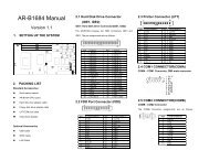
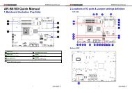
This section provides the <strong>AR</strong>-<strong>B1047</strong> hardware’ s jumpers setting, the connectors’ locations, and the pin<br />
assignment.<br />
J1<br />
2<br />
1<br />
H1<br />
1<br />
2<br />
H3 23<br />
1<br />
CN1<br />
JP1<br />
MEM5<br />
MEM4<br />
MEM3<br />
1<br />
2<br />
A B C A B C A B C<br />
M3<br />
CN2<br />
M2<br />
BAT1<br />
M1<br />
Figure 2-1 External System Location<br />
1<br />
2<br />
3<br />
SW1<br />
U4<br />
MEM2<br />
MEM1<br />
DOC<br />
H4<br />
H2<br />
2-1
<strong>AR</strong>-<strong>B1047</strong> User¡ƒs <strong>Guide</strong><br />
2.2 SYSTEM SETTING<br />
2-2<br />
Jumper pins allow you to set specific system parameters. Set them by changing the pin location of jumper blocks.<br />
(A jumper block is a small plastic-encased conductor [shorting plug] that slips over the pins.) To change a jumper<br />
setting, remove the jumper from its current location with your fingers or small needle-nosed pliers. Place the<br />
jumper over the two pins designated for the desired setting. Press the jumper evenly onto the pins. Be careful not<br />
to bend the pins.<br />
We will show the locations of the <strong>AR</strong>-<strong>B1047</strong> jumper pins, and the factory-default setting.<br />
CAUTION: 1. Do not touch any electronic component unless you are safely grounded. Wear a grounded wrist<br />
strap or touch an exposed metal part of the system unit chassis. The static discharges from your<br />
fingers can permanently damage electronic components.<br />
2. If you want to use the 12V FLASH, please use the external 12V voltage, the <strong>AR</strong>-<strong>B1047</strong> does not<br />
support the 12V voltage.<br />
2.2.1 Battery Setting<br />
(1) Battery Charge Select (JP1-1 & JP1-2)<br />
If the <strong>AR</strong>-<strong>B1047</strong> uses a 3.6V Ni-Cd rechargeable battery for SRAM data retention, the on-board charged circuit can<br />
be enabled to set JP1 jumper. The battery will be charged when the power is on.<br />
1 2 3 4 5 1 2 3 4 5<br />
Non-chargeable Battery<br />
Factory Preset<br />
Re-chargeable Battery<br />
Figure 2-2 JP1-1 & JP1-2: Battery Charge Select<br />
(2) External Battery Header (J1)<br />
J1 allows users to connect an external battery of 3.6 to 6 VDC with the <strong>AR</strong>-<strong>B1047</strong> if the on-board battery is empty.<br />
Only the SRAM disk will draw the battery current. If no SRAM chips will be used, no battery is needed. The<br />
battery charger on <strong>AR</strong>-<strong>B1047</strong> does not source charge current to the external battery connects to J1.<br />
1 Battery+<br />
2 Battery-<br />
Figure 2-3 J1: External Battery Connector
2.2.2 PC/104 Connector<br />
(1) 64 Pin PC/104 Connector Bus A & B (CN1)<br />
2<br />
1<br />
64-Pin PC/104 Connector<br />
Figure 2-4 CN1: 64-Pin PC/104 Connector Bus A & B<br />
N.C. ---<br />
SD7 ---<br />
SD6 ---<br />
SD5 ---<br />
SD4 ---<br />
SD3 ---<br />
SD2 ---<br />
SD1 ---<br />
SD0 ---<br />
N.C.---<br />
AEN ---<br />
SA19 ---<br />
SA18 ---<br />
SA17 ---<br />
SA16 ---<br />
SA15 ---<br />
SA14 ---<br />
SA13 ---<br />
SA12 ---<br />
SA11 ---<br />
SA10 ---<br />
SA9 ---<br />
SA8 ---<br />
SA7 ---<br />
SA6 ---<br />
SA5 ---<br />
SA4 ---<br />
SA3 ---<br />
SA2 ---<br />
SA1 ---<br />
SA0 ---<br />
GND ---<br />
(2) 40 Pin PC/104 Connector Bus C & D (CN2)<br />
A1<br />
A2<br />
A3<br />
A4<br />
A5<br />
A6<br />
A7<br />
A8<br />
A9<br />
A10<br />
A11<br />
A12<br />
A13<br />
A14<br />
A15<br />
A16<br />
A17<br />
A18<br />
A19<br />
A20<br />
A21<br />
A22<br />
A23<br />
A24<br />
A25<br />
A26<br />
A27<br />
A28<br />
A29<br />
A30<br />
A31<br />
A32<br />
CN1<br />
1 2<br />
B1<br />
B2<br />
B3<br />
B4<br />
B5<br />
B6<br />
B7<br />
B8<br />
B9<br />
B10<br />
B11<br />
B12<br />
B13<br />
B14<br />
B15<br />
B16<br />
B17<br />
B18<br />
B19<br />
B20<br />
B21<br />
B22<br />
B23<br />
B24<br />
B25<br />
B26<br />
B27<br />
B28<br />
B29<br />
B30<br />
B31<br />
B32<br />
--- GND<br />
--- RSTDRV<br />
--- +5 VDC<br />
--- N.C.<br />
--- N.C.<br />
--- N.C.<br />
--- N.C.<br />
--- N.C.<br />
--- +12 VDC<br />
--- N.C.<br />
--- -SMEMW<br />
--- -SMEMR<br />
--- -IOW<br />
--- -IOR<br />
--- N.C.<br />
--- N.C.<br />
--- N.C.<br />
--- N.C.<br />
--- N.C.<br />
--- N.C.<br />
--- N.C.<br />
--- N.C.<br />
--- N.C.<br />
--- N.C.<br />
--- N.C.<br />
--- N.C.<br />
--- N.C.<br />
--- N.C.<br />
--- +5 VDC<br />
--- N.C.<br />
--- GND<br />
--- GND<br />
Figure 2-5 CN1: 64-Pin PC/104 Connector Bus A & B<br />
1<br />
2<br />
40 Pin PC/104 Connector<br />
Figure 2-6 CN2: 40-Pin PC/104 Connector Bus C & D<br />
CN2<br />
GND ---<br />
N.C. ---<br />
C1<br />
C2<br />
N.C. --- C3<br />
N.C. --- C4<br />
N.C. ---<br />
N.C. ---<br />
C5<br />
C6<br />
N.C. --- C7<br />
N.C. --- C8<br />
N.C. --- C9<br />
N.C. --- C10<br />
N.C. --- C11<br />
N.C. --- C12<br />
N.C. --- C13<br />
N.C. --- C14<br />
N.C. --- C15<br />
N.C. --- C16<br />
N.C. --- C17<br />
N.C. --- C18<br />
N.C. --- C19<br />
N.C. --- C20<br />
1 2<br />
D1 --- GND<br />
D2 --- N.C.<br />
D3 --- N.C.<br />
D4 --- N.C.<br />
D5 --- N.C.<br />
D6 --- N.C.<br />
D7 --- N.C.<br />
D8 --- N.C.<br />
D9 --- N.C.<br />
D10 --- N.C.<br />
D11 --- N.C.<br />
D12 --- N.C.<br />
D13 --- N.C.<br />
D14 --- N.C.<br />
D15 --- N.C.<br />
D16 --- N.C.<br />
D17 --- +5 VDC<br />
D18 --- N.C.<br />
D19 --- GND<br />
D20 --- GND<br />
Figure 2-7 CN2: 40-Pin PC/104 Connector Bus C & D<br />
39<br />
40<br />
64<br />
63<br />
<strong>AR</strong>-<strong>B1047</strong> User¡ƒs <strong>Guide</strong><br />
2-3
<strong>AR</strong>-<strong>B1047</strong> User¡ƒs <strong>Guide</strong><br />
2.3 DIP SWITCH SETTING (SW1)<br />
2-4<br />
There is 1-DIP Switch located on the <strong>AR</strong>-<strong>B1047</strong>. If you want to use the 12V FLASH, please use the external 12V<br />
voltage, the <strong>AR</strong>-<strong>B1047</strong> does not support the 12V voltage. It performs the following functions:<br />
ON<br />
OFF<br />
1 2 3 4 5 6<br />
Figure 2-8 SW1: Switch Select<br />
SW1-1 Sets the base I/O port address<br />
SW1-2 & SW1-7 Sets the starting memory address<br />
SW1-3 & SW1-4 Sets the drive number of solid state disk<br />
SW1-5 & SW1-6 Sets the used ROM memory chips<br />
SW1-8 Set the DiskOnChip<br />
2.3.1 I/O Port Address Select (SW1-1)<br />
7 8<br />
SW1-1 is provided to select one of the two base port addresses for the solid state disk. The <strong>AR</strong>-<strong>B1047</strong> occupies 2<br />
I/O port addresses. Following state selections of base port address.<br />
SW1<br />
SW1-1 Base Port Solid State Disk<br />
OFF 224h 224h-227h<br />
ON 2A4h 2A4h-2A7h<br />
Table 2-1 I/O Port Address Select<br />
2.3.2 SSD & DiskOnChip Firmware Address Select (SW1-2, SW1-7 & SW1-8)<br />
The <strong>AR</strong>-<strong>B1047</strong>’ s SSD firmware occupies 8KB of memory. SW1-2 and SW1-7 are used to select the memory base<br />
address. You must select an appropriate address so that the <strong>AR</strong>-<strong>B1047</strong> will not conflict with memory installed on<br />
other add-on memory cards. Additionally, be sure not to use shadow RAM area or EMM driver’ s page frame in this<br />
area.<br />
SW1-2 SW1-7 SW1-8 BIOS<br />
Memory<br />
Address<br />
Bank<br />
Memory<br />
Address<br />
D.O.C.<br />
Memory<br />
Address<br />
OFF OFF OFF CC00h CE00h D000h<br />
ON OFF OFF D000h D200h D400h<br />
OFF OFF ON CC00h CE00h --<br />
ON OFF ON D000h D200h --<br />
OFF ON OFF -- CE00h CC00h<br />
ON ON OFF -- D200h D000h<br />
OFF ON ON -- -- --<br />
ON ON ON -- -- --<br />
Table 2-2 SSD Firmware Address Select<br />
If you are not going to use the solid state disk (SSD), you can adjust the SW1-7 to disable the SSD BIOS. The <strong>AR</strong>-<br />
<strong>B1047</strong> will not occupy any memory address if the SSD BIOS disabled.<br />
If you are going to install the EMM386.EXE driver, please use the [X] option to prevent EMM386.EXE from using<br />
the particular range of segment address as an EMS page is used by <strong>AR</strong>-<strong>B1047</strong>. For example, write a statement in<br />
the CONFIG.SYS file as follow: (If the memory configuration of <strong>AR</strong>-<strong>B1047</strong> is CC00:0)<br />
DEVICE=C:\DOS\EMM386.EXE X=CC00-CFFF
2.3.3 SSD Drive Number (SW1-3 & SW1-4)<br />
<strong>AR</strong>-<strong>B1047</strong> User¡ƒs <strong>Guide</strong><br />
The <strong>AR</strong>-<strong>B1047</strong>’ s SSD can simulate one or two disk drives. You can assign the drive letter of the <strong>AR</strong>-<strong>B1047</strong> by<br />
configuring SW1-3 & SW1-4.<br />
You can make the computer to boot from SSD by copying DOS into the SSD. If your SSD does not have DOS, the<br />
computer will boot from your hard disk or floppy disk. In this condition, the SSD BIOS of <strong>AR</strong>-<strong>B1047</strong> will set the<br />
drive letter of the SSD to the desired drive letter automatically.<br />
The SSD BIOS will simulate one disk drive when only (FLASH) EPROM or SRAM (starting from MEM1 socket) is<br />
installed. The drive numbers with respect to the switch setting when the <strong>AR</strong>-<strong>B1047</strong> simulates single disk drives.<br />
SW1-3 SW1-4 Occupies floppy disk number (SSD)<br />
OFF OFF 0 or 1 (Note 1)<br />
ON OFF 0 or 2 (Note 2)<br />
OFF ON 0<br />
ON ON 0<br />
Table 2-3 SSD Drive Number<br />
NOTE: 1. If there is no DOS on this SSD, the disk number will be 1 (B:). If any DOS is found by the <strong>AR</strong>-<strong>B1047</strong><br />
SSD BIOS, the disk number will be 0 (A:) But, you can change the disk number from 0 to 1 by pressing<br />
the key during system bootup.<br />
2. If there is no DOS on this SSD, the disk number will be 2 (C: or D: or …). If any DOS is found by the<br />
<strong>AR</strong>-<strong>B1047</strong> SSD BIOS, the disk number will be 0 (A:). But, you can change the disk number from 0 to 2<br />
by pressing the key during system bootup.<br />
(1) Simulate 2 Disk Drive<br />
When (FLASH) EPROM and SRAM are both used on the <strong>AR</strong>-<strong>B1047</strong>, or you only have installed SRAM that does<br />
not start from MEM1 socket, the <strong>AR</strong>-<strong>B1047</strong> will simulate two disk drives. The drive numbers respect to those<br />
switch settings when <strong>AR</strong>-<strong>B1047</strong> simulates two disk drives.<br />
SW1-3 SW1-4<br />
Occupies floppy disk number<br />
FLASH (EPROM) SRAM<br />
OFF OFF 0 or 1 (Note 1) 2<br />
ON OFF 0 or 2 (Note 2) 3<br />
OFF ON 0 1<br />
ON ON 0 2<br />
Table 2-4 SSD Drive Number for Simulate 2 Disk Drives<br />
NOTE: 1. If there is no DOS on this SSD, the disk number will be 1 (B:). If any DOS is found by the <strong>AR</strong>-<strong>B1047</strong><br />
SSD BIOS, the disk letter will be 0 (A:). But, you can change the disk number from 0 to 1 by pressing<br />
the key during system bootup.<br />
2. If there is no DOS on this SSD, the disk number will be 2 (C: or D: or …). If any DOS is found by the<br />
<strong>AR</strong>-<strong>B1047</strong> SSD BIOS, the disk number will be 0 (A:). But, you can change the disk number from 0 to 2<br />
by pressing the key during system bootup.<br />
2-5
<strong>AR</strong>-<strong>B1047</strong> User¡ƒs <strong>Guide</strong><br />
(2) Disk Drive Name Arrangement<br />
If any logical hard disk drives exist in your system, there will also be a different disk number depending on which<br />
version DOS you are using.<br />
The solid state disk drive number with there respective DOS drive designation are listed in table as follows.<br />
2-6<br />
Condition<br />
Floppy disk No. Logical hard disk<br />
0 1 2 3 1 2 3 4<br />
No Logical hard disk A: B: C: D: -- -- -- --<br />
1 Logical hard disk A: B: C: D: E: -- -- --<br />
2 Logical hard disk A: B: C: D: E: F: -- --<br />
3 Logical hard disk A: B: C: D: E: F: G: --<br />
4 Logical hard disk A: B: C: D: E: F: G: H:<br />
Table 2-5 SSD Drive Number for DOS Version before 5.0<br />
Condition<br />
Floppy disk No. Logical hard disk<br />
0 1 2 3 1 2 3 4<br />
No Logical hard disk A: B: C: D: -- -- -- --<br />
1 Logical hard disk A: B: D: E: C: -- -- --<br />
2 Logical hard disk A: B: E: F: C: D: -- --<br />
3 Logical hard disk A: B: F: G: C: D: E: --<br />
4 Logical hard disk A: B: G: H: C: D: E: F:<br />
Table 2-6 SSD Drive Number for DOS Version 5.0 and Newer<br />
2.3.4 ROM Type Select (SW1-5 & SW1-6)<br />
SW1-5 & SW1-6 are used to select the memory type of ROM disk section. If you want to use the 12V FLASH,<br />
please use the external 12V voltage, the <strong>AR</strong>-<strong>B1047</strong> does not support the 12V voltage.<br />
SW1-5 SW1-6 EPROM Type<br />
OFF OFF UV EPROM (27Cxxx)<br />
ON OFF 5V FLASH 29Fxxx<br />
OFF ON 5V FLASH(29Cxxx & 29EExxx)(*Note)<br />
ON ON 12V FLASH (28Fxxx)<br />
Table 2-7 ROM Type Select<br />
NOTE: It is also supported 28EExxx 5V FLASH, the BIOS message will still show 5V FLASH (29Cxxx or 29EExxx)<br />
disk.
2.4 MEMORY TYPE SETTING (M1, M2 & M3)<br />
<strong>AR</strong>-<strong>B1047</strong> User¡ƒs <strong>Guide</strong><br />
Before installing the memory into memory sockets MEM1 through MEM5, you have to configure the memory type<br />
which will be used (ROM/RAM) on the <strong>AR</strong>-<strong>B1047</strong>. You can configure the <strong>AR</strong>-<strong>B1047</strong> as a EPROM (FLASH) disk<br />
(ROM only), a SRAM disk (SRAM only) or a combination of EPROM (FLASH) and SRAM disk.<br />
It is not necessary to insert memory chips into all of the sockets. The number of SRAM chips required depends on<br />
your RAM disk capacity. The number of EPROM chips required depends on the total size of files that you plan to<br />
copy onto the ROM disk and whether or not it will be bootable.<br />
Insert the first memory chip into MEM1 if you are going to configure it as a ROM or SRAM disk. If you use a<br />
combination of ROM and RAM, then insert the EPROM (FLASH) chip first from MEM1 and insert the SRAM from<br />
the first socket is set as SRAM.<br />
The M1 jumper block is used to configure the memory type of MEM1 and MEM2, M2 is for MEM3 and MEM4, M3<br />
is for MEM5. Please refer to the following chart to select the correct memory type.<br />
� M1:is used to configure the memory type of MEM1 & MEM2<br />
� M2:is used to configure the memory type of MEM3 & MEM4<br />
� M3:is used to configure the memory type of MEM5<br />
CAUTION: When the power is turned off, please note the following precautions.<br />
1. If your data has been stored in the SRAM disk, do not change the jumper position or data will be<br />
lost.<br />
2. Make sure jumpers are set properly. If you mistakenly set the jumpers for SRAM and you have<br />
EPROM or FLASH installed, the EPROM or FLASH will drain the battery’ s power.<br />
3. If you want to use the 12V FLASH, please use the external 12V voltage, the <strong>AR</strong>-<strong>B1047</strong> does not<br />
support the 12V voltage.<br />
1<br />
2<br />
3<br />
M1, M2, & M3<br />
1<br />
2<br />
3<br />
A B C<br />
M1, M2, & M3<br />
1<br />
2<br />
3<br />
A B C<br />
M1, M2, & M3<br />
1<br />
2<br />
3<br />
A B C<br />
A B C<br />
M1, M2, & M3<br />
1 2 3<br />
1 2 3 4 5<br />
EPROM (128KX8, 256KX8 and 512KX8)<br />
5V/12V FLASH (64KX8, 128KX8 and 256KX8)<br />
(Factory Preset)<br />
1 2 3 4 5<br />
5V FLASH (512KX8 Only)<br />
SRAM<br />
JP1<br />
4 5<br />
1MX8 EPROM (Only)<br />
JP1<br />
JP1<br />
JP1<br />
1 2 3<br />
4 5<br />
Figure 2-9 M1~M3 & JP1-3~JP1-5: Memory Type Setting<br />
2-7
3. INSTALLATION<br />
<strong>AR</strong>-<strong>B1047</strong> User¡ƒs <strong>Guide</strong><br />
The chapter describes the various type SSDs’ installation steps as follows. The jumper and switch adjust as SSD’ s<br />
different type to set.<br />
� Overview<br />
� ROM Disk Installation<br />
� Using the Write Protect Function<br />
� Memory Device Supported<br />
� How to Use the D.O.C.<br />
CAUTION: When the power is turned off, please note the following precautions.<br />
1. If your data has been stored in the SRAM disk, do not change the jumper position or data will be<br />
lost.<br />
3.1 OVERVIEW<br />
2. Make sure jumpers are set properly. If you mistakenly set the jumpers for SRAM and you have<br />
EPROM or FLASH installed, the EPROM or FLASH will drain the battery’ s power.<br />
3. If you want to use the 12V FLASH, please use the external 12V voltage, the <strong>AR</strong>-<strong>B1047</strong> does not<br />
support the 12V voltage.<br />
This chapter provides information for you to set up a working system based on the <strong>AR</strong>-<strong>B1047</strong> card. Please read<br />
the details of the card’ s hardware descriptions before installation carefully, especially jumper settings and cable<br />
connections.<br />
Follow steps listed below for proper installation:<br />
Step 1 : Make sure the base I/O address does not conflict with other I/O cards.<br />
Step 2 : Make sure the memory address does not conflict with other memory cards.<br />
Step 3 : Make sure the jumper settings for the memory are all installed properly.<br />
Step 4 : Don’ t use the shadow RAM on the firmware address.<br />
Step 5 : If you have installed an EMS driver, don’ t use the same range of memory address as the <strong>AR</strong>-<strong>B1047</strong>.<br />
Step 6 : If you are using the MS-DOS 6.2 to format SRAM or small page 5V FLASH disk, you might get some bad<br />
sectors in your FLASH/RAM disk. This will reduce the capacity of your FLASH/RAM disk. To solve this<br />
problem, please type:<br />
C:\>FORMAT [FLASH/SRAM disk letter] /S/U/C<br />
or<br />
C:\>FORMAT [FLASH/SRAM disk letter] /U/C<br />
3.2 ROM <strong>DISK</strong> INSTALLATION<br />
To support the <strong>AR</strong>-<strong>B1047</strong> solid state disk’ s operations, the following files has been provided some functions as<br />
follows:<br />
(A) PGM1047.EXE<br />
PGM1047.EXE PGM1047.EXE is used to program the 12V FLASH EPROM after the ROM pattern files are<br />
generated by RFG.EXE. The PGM1047.EXE can also program the correctness of the ROM<br />
pattern files onto 5V FLASH EPROM (start from MEM1) or SRAM for testing the ROM pattern files.<br />
3-1
<strong>AR</strong>-<strong>B1047</strong> User¡ƒs <strong>Guide</strong><br />
3-2<br />
To execute PGM1047.EXE, the main menu will be displayed on your screen. There are 8 options on the main<br />
menu.<br />
Quit to DOS<br />
Quits and exits to the DOS.<br />
OS Shell<br />
Exits from PGM1047 temporarily to the DOS prompt. Type EXIT to return to PGM1047 main menu.<br />
Load ROM File<br />
If this option is used, the PGM1047 will prompt you for the ROM pattern file name. This option is useful if you<br />
have not previously entered a ROM pattern file name or if you wish to use a different ROM pattern file. The<br />
PGM1047 will check and display the ROM file name, ROM file size, (FLASH) memory capacity and the number<br />
of ROM pattern files that will be loaded and copied onto the (FLASH) memory chips.<br />
Verify Memory<br />
If ROM pattern files were loaded without error, this option instructs PGM1047 to verify the contents of (FLASH)<br />
memory chips with the current ROM pattern files.<br />
Program Memory<br />
If there are no mistakes in your ROM pattern file, then this menu option will erase (FLASH) memory, write the<br />
current ROM pattern files onto (FLASH) memory and verify data that was just written to (FLASH) memory, using<br />
the ROM pattern files.<br />
Memory Type/Mfr.<br />
Before you program the (FLASH) memory chips, make sure that the FLASH’ s type and manufactory match the<br />
one shown on the main menu. Otherwise, you can use this option to select the proper type and manufacture<br />
and instruct the program to use a right programming algorithm.<br />
Select PGM Chips<br />
Normally the PGM1047 will program all ROM pattern files onto the FLASH memories with the ROM pattern files<br />
just loaded. But you can use this option to select which memory chips that you want to program and which<br />
memory chips need to be skipped. The PGM1047 will only program the selected chips when writing data to the<br />
FLASH memory. This is very useful when some of the memory chip were verified and programmed previously.<br />
Select FLASH PLSCNTs<br />
If the 12V FLASHs have been programmed several times, please select the FLASH PLSCNT mode<br />
instead of mode. In the or mode, PGM1047.EXE will retry more times to<br />
program data onto the 12V FLASHs correctly.<br />
The default setting is mode.<br />
(B) WP1047.EXE<br />
WP1047.EXE This program demonstrates how to enable and disable software writes protect function. It also<br />
shows the current protect mode of write or read only memory.
<strong>AR</strong>-<strong>B1047</strong> User¡ƒs <strong>Guide</strong><br />
(C) RFG.EXE<br />
RFG.EXE This program is used to generate ROM pattern files in a binary format. Each ROM pattern file has<br />
the same size as the FLASH or EPROM and can be easily programmed on to the FLASH with onboard<br />
programmer or on to EPROM with any EPROM programmer. If you have specified a DOS<br />
drive in the *.PGF file, RFG will generate bootable ROM pattern files for the EPROM or FLASH<br />
disk. The RFG supports the following DOS: MS-DOS, PC-DOS, DR-DOS, and X-DOS.<br />
NOTE: If you want to use <strong>AR</strong>-<strong>B1047</strong> with any DOS which is not supported by RFG, please send your requirement<br />
to <strong>Acrosser</strong> Technology Co., Ltd. or contract with your local sales representative.<br />
The RFG.EXE provided in the utility diskette is a program that converts the files you list in the PGF and convert<br />
them into ROM pattern file. The RFG will determine how many EPROMs are needed and generate the same<br />
number of ROM pattern files. These ROM pattern files are named with the name assigned by the ROM_NAME in<br />
the PGF and the extension names are *.R01, *.R02 …etc. To generate ROM pattern files.<br />
The ROM File Generator main menu will be displayed on the screen. There are 7 options on the main menu. They<br />
serve the following functions:<br />
Quit to DOS<br />
Quits and exits to the DOS<br />
OS Shell<br />
Exits from the RFG temporarily to the DOS prompt. Type to return to the RFG main menu.<br />
Load PFG File<br />
If this option is used, the RFG will prompt you for the PGF file name. This option is useful if you have not<br />
previously entered a PGF name or you wish to use a different PGF file. The RFG will check and display the<br />
PGF filename, ROM pattern file name, EPROM’ s capacity, DOS version and the number of ROM pattern files<br />
that will be generated.<br />
Type Current PGF File<br />
This option instructs the RFG to use the DOS type command to display the contents of the current PGF file.<br />
Generate ROM File(s)<br />
If there is no mistake in your *.PGF file, then this menu option will generate ROM pattern files. The number of<br />
ROM pattern file generated by the RFG will depend on the total capacity needed by your files. For instance, if 3<br />
files are generated, then you will need to use 3 EPROMs (The size depends upon the number stated in your<br />
PGF). The ROM pattern files will have the same file names, but will have different extension names. For<br />
example:<br />
TEST.R01, TEST.R02, TEST.R03 tc.<br />
Display Error in PGF File<br />
This option displays errors that were detected in your PGF.<br />
Help to PGF File<br />
This option gives information on how to write a PGF file and how to generate ROM pattern files. An example<br />
PGF is also included.<br />
Move the reverse video bar to then press [ENTER]. The ROM pattern file is a binary<br />
file. The file size will be the same size as the EPROM that you assigned in the PGF. For example, if you are<br />
using 128KX8 EPROM memory chips, then the size of ROM patterns file will be 131072 bytes. For other chips<br />
the file size will be:<br />
64KX8 EPROM----65536 bytes<br />
256KX8 EPROM¡ X262144 bytes<br />
512KX8 EPROM---524288 bytes<br />
1MX8 EPROM -----1048576 bytes<br />
3-3
<strong>AR</strong>-<strong>B1047</strong> User¡ƒs <strong>Guide</strong><br />
(D) RFGDEMO.PGF<br />
RFGDEMO.PGF This file provides a sample PROGRAM GROUP FILE which illustrates how to create ROM pattern<br />
files correctly.<br />
3-4<br />
The PGF is an ASCII text file that can be created by using any text editor, word processor or DOS <br />
command. The PGF lists what files will be copied and if DOS is going to be copied. This file can have any DOS<br />
filename, but the extension name must be *.PGF. For example, followings are valid filenames.<br />
RFGDEMO.PGF<br />
MYRFG.PGF<br />
MSDOS.PGF<br />
…<br />
An examples of the *.PGF file is as follow.<br />
ROM_NAME=TEST1 ; ROM pattern file name is TEST1<br />
;The output file names will be TEST1.R01,<br />
;TEST1.R02...etc.<br />
DOS_DRIVE=C: ; DOS system drive unit is drive C:<br />
;If user does not want to copy DOS<br />
;system files onto the ROM disk<br />
;write as DOS_DRIVE=NONE<br />
ROM_SIZE=128 ;64 means 64KX8 (28F512) EPROM<br />
;size used<br />
;128 means 128KX8 (27C/28F/29F010)<br />
;EPROM size used<br />
;256 means 512KX8 (27C/28F/29F020)<br />
;EPROM size used<br />
;512 means 512KX8 (27C/29F040)<br />
;EPROM size used<br />
;1024 means 1MX8 (27C080) EPROM<br />
;size used<br />
The following two files are options which depend on whether the ROM disk is to be bootable or not.<br />
CONFIG.SYS<br />
AUTOEXEC.BAT<br />
;Below are user’ s files<br />
A:\USER1.COM ; File USER1.COM on root of drive A:<br />
USER2.EXE ; File USER2.EXE on current directory & drive<br />
C:\TTT\USER3.TXT ; File USER3.TXT on sub-directory TTT of drive C:
3.2.1 UV EPROM (27Cxxx)<br />
(1) Switch and Jumper Setting<br />
Step 1: Use jumper block to set the memory type as ROM (FLASH).<br />
Step 2: Use jumper JP1 to select the correct EPROM type if 1Mx8 (27C080) EPROM is used.<br />
<strong>AR</strong>-<strong>B1047</strong> User¡ƒs <strong>Guide</strong><br />
Step 3: Select the proper I/O base port, firmware address, disk drive number and EPROM type on SW1.<br />
Step 4: Insert programmed EPROM(s) or FLASH(s) chips into sockets starting at MEM1.<br />
Step 5: Line up and insert the <strong>AR</strong>-<strong>B1047</strong> card into any free slot of your computer.<br />
1<br />
2<br />
3<br />
1<br />
2<br />
3<br />
ON<br />
OFF<br />
1 2 3 4 5 6 7 8<br />
Figure 3-1 UV EPROM (27CXXX) Switch Setting<br />
A B C<br />
M1, M2, & M3<br />
A B C<br />
M1, M2, & M3<br />
JP1<br />
1 2 3<br />
1MX8 EPROM (Only)<br />
JP1<br />
1 2 3<br />
4<br />
5<br />
EPROM (128KX8, 256KX8 and 512KX8)<br />
Figure 3-2 M1~M3 & JP1-3~JP1-5: UV EPROM Jumper Setting<br />
(2) Software Programming<br />
Use the UV EPROM, please refer to the follow steps:<br />
Step 1: Turn on power and boot DOS from hard disk drive or floppy disk drive.<br />
Step 2: Making a Program Group File (*.PGF file)<br />
4<br />
Step 3: Using the RFG.EXE to generate ROM pattern files, and counting the ROM numbers as the pattern files.<br />
Step 4: In the DOS prompt type the command as follows.<br />
C:\>RFG [file name of PGF]<br />
Step 5: In the RFG.EXE main menu, choose the item, that is user editing *.PGF file.<br />
5<br />
Step 6: Choose the , the tools program will generate the ROM files, for programming the<br />
EPROMs.<br />
Step 7: Program the EPROMs<br />
Using the instruments of the EPROM writer to load and write the ROM pattern files into the EPROM chips.<br />
Make sure that the EPROMs had been verified by the programming without any error.<br />
3-5
<strong>AR</strong>-<strong>B1047</strong> User¡ƒs <strong>Guide</strong><br />
3-6<br />
Step 8: Install EPROM chips<br />
Be sure to place the programmed EPROMs (R01, R02 …) into socket starting from MEM1 and ensure that<br />
the chips are installed in the sockets in the proper orientation.<br />
3.2.2 12V or Large Page 5V FLASH Disk<br />
If you are using 12V FLASH or large page 5V FLASH as ROM disk, it is the same procedure as step 1 to step 4 of<br />
using the UV EPROM.<br />
CAUTION: If you want to use the 12V FLASH, please use the external 12V voltage, the <strong>AR</strong>-<strong>B1047</strong> does not<br />
support the 12V voltage.<br />
(1) Switch and Jumper Setting<br />
Step 1: Use jumper block to set the memory type as ROM (FLASH).<br />
Step 2: Use jumper JP1 to select the correct EPROM/FLASH type.<br />
Step 3: Select the proper I/O base port, firmware address, disk drive number and EPROM/FLASH type on SW1.<br />
Step 4: Insert programmed EPROM(s) or FLASH(s) chips into sockets starting at MEM1.<br />
Step 5: Line up and insert the <strong>AR</strong>-<strong>B1047</strong> card into any free slot of your computer.<br />
Step 6: If 12V FLASH or large page 5V FLASH is being installed for the first time, use the FLASH programming<br />
utility PGM1047.EXE to program ROM pattern files, which have been generated by RFG.EXE, onto the<br />
FLASH chips.<br />
ON<br />
OFF<br />
1 2 3 4 5 6 7 8<br />
Figure 3-3 5V Large FLASH (29FXXX) Switch Setting<br />
ON<br />
OFF<br />
1 2 3 4 5 6 7 8<br />
Figure 3-4 12V FLASH (28FXXX) Switch Setting
1<br />
2<br />
3<br />
1<br />
2<br />
3<br />
A B C<br />
M1, M2, & M3<br />
A B C<br />
M1, M2, & M3<br />
1 2 3<br />
5V/12V FLASH (64KX8, 128KX8 and 256KX8)<br />
(Factory Preset)<br />
1 2 3<br />
JP1<br />
JP1<br />
4<br />
4<br />
5V FLASH (512KX8 Only)<br />
Figure 3-5 M1~M3 & JP1-3~JP1-5: 12V or Large Page 5V FLASH Jumper Setting<br />
(2) Software Programming<br />
And then, you should create a PGF and generate ROM pattern files by using the RFG.EXE.<br />
Step 1: Making a Program Group File (*.PGF file)<br />
Step 2: Generate ROM pattern files<br />
Step 3:<br />
Step 4:<br />
Turn off your system, and then install FLASH EPROMs into the sockets.<br />
5<br />
5<br />
<strong>AR</strong>-<strong>B1047</strong> User¡ƒs <strong>Guide</strong><br />
NOTE: Place the appropriate number of FLASH EPROM chips (the numbers depends on the ROM pattern<br />
files generated by RFG.EXE) into the socket starting from MEM1 and ensure that the chips are<br />
installed in the sockets in the proper orientation. Line up and insert the <strong>AR</strong>-<strong>B1047</strong> board into any<br />
free slot of your computer.<br />
Turn on your system, and Program FLASH EPROMs.<br />
NOTE: The FLASH EPROM program is built-in the <strong>AR</strong>-<strong>B1047</strong> board. The FLASH EPROMs can be<br />
programmed on the <strong>AR</strong>-<strong>B1047</strong>. Before programming the FLASH EPROMs, please insert at least<br />
the same number of FLASH EPROMs, please insert at least the same number of FLASH EPROMs,<br />
please insert at least the same number of FLASH chips as the ROM pattern files generated.<br />
Step 5: The PGM1047.EXE file is a program that loads and writes the ROM pattern files onto the (FLASH) memory<br />
chips. To program the FLASH EPROM.<br />
Step 6: In the DOS prompt type the command as follows.<br />
C:\>PGM1047 [ROM pattern file name]<br />
Step 7: In the main menu, choose the item, that is the ROM_NAME=[file name] in the *.PGF file.<br />
Step 8:<br />
Step 9:<br />
Choose the item, this item program will program the EPROMs.<br />
NOTE: Move the reverse video bar to the option then press . PGM1047 will write<br />
the ROM pattern files onto the (FLASH) memories. Ensure that data is verified by the PGM1047<br />
correctly.<br />
Reboot the system<br />
NOTE: Reboot your computer by making a software or hardware reset.<br />
3-7
<strong>AR</strong>-<strong>B1047</strong> User¡ƒs <strong>Guide</strong><br />
3.2.3 Small Page 5V FLASH ROM Disk<br />
(1) Switch and Jumper Setting<br />
3-8<br />
Step 1: Use jumper block to set the memory type as ROM (FLASH).<br />
Step 2: Use jumper JP1 to select the correct EPROM type.<br />
Step 3: Select the proper I/O base port, firmware address, disk drive number and EPROM type on SW1.<br />
Step 4: Insert programmed EPROM(s) or FLASH(s) chips into sockets starting at MEM1.<br />
Step 5: Line up and insert the <strong>AR</strong>-<strong>B1047</strong> card into any free slot of your computer.<br />
Step 6: If 5V FLASH (small page) is being used for the first., use the DOS command FORMAT to format the FLASH<br />
disk:<br />
C:\>FORMAT [ROM disk letter] /S /U<br />
or<br />
C:\>FORMAT [ROM disk letter] /U<br />
ON<br />
OFF<br />
1 2 3 4 5 6 7 8<br />
Figure 3-6 5V FLASH (29CXXX & 29EEXXX) Switch Setting<br />
1<br />
2<br />
3<br />
1<br />
A B C<br />
M1, M2, & M3<br />
A B C<br />
1 2 3<br />
JP1<br />
4<br />
5<br />
5V/12V FLASH (64KX8, 128KX8 and 256KX8)<br />
(Factory Preset)<br />
JP1<br />
2<br />
3<br />
1 2 3 4 5<br />
M1, M2, & M3<br />
5V FLASH (512KX8 Only)<br />
Figure 3-7 M1~M3 & JP1-3~JP1-5: 5V FLASH (29CXXX & 29EEXXX) Jumper Setting<br />
(2) Using Tool Program<br />
If small page 5V FLASH EPROMs are used, you can use the same method as 12V FLASH EPROMs, it is the<br />
same procedure as step 1 to step 4 of using the UV EPROM:<br />
Step 1: Making a Program Group File (*.PGF file)<br />
Step 2: Generating ROM pattern files<br />
Step 3: Installing FLASH EPROMs<br />
Step 4: Programming FLASH EPROMs<br />
Step 5: Reboot system
<strong>AR</strong>-<strong>B1047</strong> User¡ƒs <strong>Guide</strong><br />
(3) Typing DOS Command<br />
You can use another way to format and copy files to the 5V FLASH EPROM. This method provides the<br />
convenience of using a RAM disk. You can use the DOS and command to format and copy<br />
files. Follow the steps to format and copy files to the FLASH disk. It is the same procedure as step 1 to step 4 of<br />
using the UV EPROM.<br />
Step 1: Turn on your computer, when the screen shows the SSD BIOS menu, please hit the [F1] key during the<br />
system boot-up, this enables you to enter the FLASH setup program. If the program does not show up,<br />
check the switch setting of SW1.<br />
Step 2: Use , , , and arrow keys to select the correct FLASH memory type<br />
and how many memory chips are going to be used.<br />
Step 3: Press the [F4] key to save the current settings.<br />
Step 4: After the DOS is loaded, use the DOS [FORMAT] command to format the FLASH disk.<br />
To format the disk and copy DOS system files to the disk.<br />
C:\>FORMAT [ROM disk letter] /S /U<br />
To format the disk without copying DOS system files.<br />
C:\>FORMAT [ROM disk letter] /U<br />
Step 5: Copy your program or files to the FLASH disk by using DOS [COPY] command.<br />
CAUTION: It is not recommended that the users format the disk and copy files to the FLASH disk very often.<br />
Since the FLASH EPROMs write cycle life time is about 10,000 or 100,000 times, writing data to the<br />
FLASH too often will reduce the life time of the FLASH EPROM chips, especially the FLASH EPROM<br />
chip in the MEM1 socket.<br />
3.2.4 RAM Disk<br />
(1) Jumper Setting<br />
Step 1: Use jumper block to set the memory type as SRAM.<br />
Step 2: Select the proper I/O base port, firmware address, disk drive number on SW1.<br />
Step 3: Insert programmed SRAM chips into sockets starting at MEM1.<br />
Step 4: Line up and insert the <strong>AR</strong>-<strong>B1047</strong> card into any free slot of your computer.<br />
Step 5: Use the DOS command FORMAT to format the RAM disk. If you are installing SRAM for the first time:<br />
C:\>FORMAT [RAM disk letter] /S /U<br />
or<br />
C:\>FORMAT [RAM disk letter] /U<br />
NOTE: If you use the SRAM, please skip the SW1-5 & SW1-6 setting.<br />
3 2 1<br />
A<br />
B<br />
C<br />
M1, M2, & M3<br />
JP1<br />
1 2 3<br />
SRAM<br />
Figure 3-8 SRAM Jumper Setting<br />
4<br />
5<br />
3-9
<strong>AR</strong>-<strong>B1047</strong> User¡ƒs <strong>Guide</strong><br />
(2) Software Programming<br />
It is very easy to use the RAM disk. The RAM disk operates just like a normal floppy disk. A newly installed RAM<br />
disk needs to be formatted before files can be copied to it. Use the DOS command [FORMAT] to format the RAM<br />
disk.<br />
3-10<br />
Step 1: Use jumper block to select the memory type as SRAM refer.<br />
Step 2: Select the proper I/O base port, firmware address and disk drive number on SW1.<br />
Step 3: Insert SRAM chips into sockets starting from MEM1<br />
Step 4: Turn on power and boot DOS from hard disk drive or floppy disk drive.<br />
Step 5: Use the DOS command [FORMAT] to format the RAM disk. If you are installing SRAM for the first time.<br />
To format the RAM disk and copy DOS system files onto the RAM disk.<br />
C:\>FORMAT [RAM disk letter] /S /U<br />
To format the RAM disk without copying DOS system files into the RAM disk.<br />
C:\>FORMAT [RAM disk letter] /U<br />
Step 6: Use the DOS command [COPY] to copy files onto the RAM disk. For example, if you want to copy file<br />
to the RAM disk from drive C: and the RAM disk is assigned as drive A:.<br />
COPY C:EDIT.EXE A:<br />
NOTE: In addition, you can use any other DOS command to operate the RAM disk.<br />
3.2.5 Combination of ROM and RAM Disk<br />
The <strong>AR</strong>-<strong>B1047</strong> can be configured as a combination of one ROM disk and one RAM disk. Each disk occupies a<br />
drive unit.<br />
Step 1: Use jumper block to select the proper ROM/RAM configuration you are going to use.<br />
Step 2: Insert the first programmed EPROM into the socket MEM1, the second into the socket MEM2, etc.<br />
Step 3: Insert the SRAM chips starting from the first socket assigned as SRAM.<br />
Step 4: Select the proper I/O base port, firmware address and disk drive number on SW1.<br />
Step 5: Turn on power and boot DOS from hard disk drive or floppy disk drive.<br />
Step 6: Use the DOS command [FORMAT] to format the RAM disk.<br />
C:\>FORMAT [RAM disk letter] /U<br />
Step 7: If 5V FLASH (small page) is being used for the first time.<br />
And then use the DOS command [FORMAT] to format the FLASH disk.<br />
Step 8: If 12V FLASH or large page 5V FLASH is being installed for the first time, please use the FLASH<br />
programming utility PGM1047.EXE to program ROM pattern files, which have been generated by RFG.EXE<br />
onto the FLASH chips.<br />
NOTE: Users can only boot DOS from the ROM disk drive if the <strong>AR</strong>-<strong>B1047</strong> is configured as a ROM and a RAM<br />
disk. You don’ t need to copy DOS onto the RAM disk.
3.3 USING THE WRITE PROTECT FUNCTION<br />
<strong>AR</strong>-<strong>B1047</strong> User¡ƒs <strong>Guide</strong><br />
The <strong>AR</strong>-<strong>B1047</strong> provides software write protect functions for small page 5V FLASH disk and only software write<br />
protect function for SRAM disk to prevent your data on 5V FLASH or SRAM disk from accidental deletion or<br />
overwrite. If your FLASH/SRAM disk is write protected, any write operation to the protected FLASH/SRAM disk will<br />
get a write protect error<br />
Write protect error writing drive A<br />
Abort, Retry, Fail?<br />
If you need the write protect function and sometimes you have to write or update data on your FLASH/SRAM disk,<br />
you can use the software write protect instead of hardware write protect. The software write protect function is<br />
enabled or disabled by writing data to an I/O port.<br />
(1) Enable the Software Write Protect<br />
Writes 80H to the base port+0 address<br />
Example 1: (in assembly language)<br />
MOV DX,224H ; If the <strong>AR</strong>-1047’ s base I/O address is 224H<br />
MOV AL,80H ; Enable byte=80H<br />
OUT DX,AL<br />
Example 2: (in BASICA language)<br />
OUT &H224,&H80 : REM If the <strong>AR</strong>-<strong>B1047</strong>’ s base I/O address is 224H<br />
Example 3: (in Turbo C language)<br />
outportb(0x224,0x80) ; /*If the <strong>AR</strong>-<strong>B1047</strong>’ s base I/O address is 224H*/<br />
(2) Disable the Software Write Protect<br />
Writes 0H to the base port+0 address<br />
Example 1: (in assembly language)<br />
MOV DX,224H ; If the <strong>AR</strong>-1047’ s base I/O address is 224H<br />
MOV AL,00H ; Disable byte=00H<br />
OUT DX,AL<br />
Example 2: (in BASICA language)<br />
OUT &H224,&H00 : REM If the <strong>AR</strong>-<strong>B1047</strong>’ s base I/O address is 224H<br />
Example 3: (in Turbo C language)<br />
outportb(0x224,0x00) ; /*If the <strong>AR</strong>-<strong>B1047</strong>’ s base I/O address is 224H*/<br />
3-11
<strong>AR</strong>-<strong>B1047</strong> User¡ƒs <strong>Guide</strong><br />
3.4 MEMORY DEVICE SUPPORTED<br />
3-12<br />
Five 32-pin JEDEC memory sockets on the <strong>AR</strong>-<strong>B1047</strong> can be populated with up to 5MB of EPROM, 2.5MB of<br />
FLASH, 2.5MB of SRAM or combinations the EPROM/SRAM or FLASH/SRAM. Each socket accepts the following<br />
memory chips:<br />
EPROM: 27C080 (1MX8), 27C040 (512KX8), 27C020 (256KX8), and 27C010 (128KX8)<br />
Small Page 5V FLASH: 29C040A (512KX8), 29C040 (512KX8), 29C020 (256KX8), 29C010 (128KX8), 29C512 (64KX8),<br />
28EE010 (128KX8), 28EE011 (128KX8), 29EE010 (128KX8), 29EE011 (128KX8), and 28SF040<br />
(512KX8)<br />
Large Page 5V FLASH: 29F040 (512KX8), 29F020 (256KX8), 29F010 (128KX8), and 29F512 (64KX8)<br />
12V FLASH: 28F020 (256KX8), 28F010 (128KX8), and 28F512 (64KX8)<br />
SRAM: 584000 (512KX8), 581000 (128KX8)<br />
The <strong>AR</strong>-<strong>B1047</strong> uses a 3.6 volts Lithium non-chargeable battery to backup stored data in the SRAM memory when<br />
the power is off. Please use low power SRAM chips for a longer data retention period. (These SRAM chips are<br />
usually designated with a “ L” in the chip model code.)<br />
CAUTION: If you want to use the 12V FLASH, please use the external 12V voltage, the <strong>AR</strong>-<strong>B1047</strong> does not<br />
support the 12V voltage.<br />
3.5 HOW TO USE THE D.O.C.<br />
This section provides the information about how to use the D.O.C. (DiskOnChip).<br />
Step 1: Use SW1-8 set the DiskOnChip to Enable or Disable.<br />
Step 2: Insert programmed DiskOnChip into sockets DOC.<br />
Step 3: Line up and insert the <strong>AR</strong>-<strong>B1047</strong> card into any free slot of your computer.<br />
ON<br />
OFF<br />
1 2 3 4 5 6 7 8<br />
Figure 3-9 D.O.C. Switch Setting
4. HOW TO USE THE MEMORY BANKS<br />
<strong>AR</strong>-<strong>B1047</strong> User¡ƒs <strong>Guide</strong><br />
This section provides the information about how to access the memory on the <strong>AR</strong>-<strong>B1047</strong> without using the <strong>AR</strong>-<br />
<strong>B1047</strong> SSD BIOS. The <strong>AR</strong>-<strong>B1047</strong> hardware cut every 8K bytes of memory into a memory bank. To access the<br />
data in memory, you have to assign the chip number and the bank number. On every chip, the memory bank<br />
number starts from the number zero. The last memory bank number depends on the size of the memory chip used<br />
on the <strong>AR</strong>-<strong>B1047</strong>. For example, if you use the 256K bytes memory chip, the bank number on every chip would be<br />
in the range of 0 to 31. The chip number and the bank number are determined by the bank selected register and<br />
the chip selected register on the <strong>AR</strong>-<strong>B1047</strong>.<br />
The I/O address of these registers is determined by SW1-1. The memory address of the memory bank is located<br />
on the range selected by SW1-2 and SW1-7. Please refer to the how to select the I/O port address and the<br />
memory address of the memory bank.<br />
The I/O port address of the bank select register is base port+0 and the I/O port address of the chip select register<br />
is base port + 2. The following is the format of the bank select register and chip select register.<br />
Register I/O Port D7 D6 D5 D4 D3 D2 D1 D0<br />
Bank Select<br />
Register<br />
Base+0 WPE A6 A5 A4 A3 A2 A1 A0<br />
Chip Select<br />
Register<br />
Base+2 0 0 0 0 0 CS2 CS1 CS0<br />
Table 4-1 The Format of the Memory Bank<br />
Where:<br />
WPE Write protect enable bit (refer to section “ Using the Write<br />
Protect Function” for details)<br />
A6 ¡ V A0 Bank select bits, A0 is the LSB.<br />
CS2 ¡ V CS0 Chip select bits of MEM1 to MEM8, CS0 is the LSB.<br />
For different types of memory, A0 to A6 have different explanations. These bits are used to select the bank<br />
number of specific memory located by CS0 to CS2.<br />
Memory A6 A5 A4 A3 A2 A1 A0<br />
64KB EPROM/FLASH 0 0 1 0 BS2 BS1 BS0<br />
128KB EPROM/FLASH 0 0 1 BS3 BS2 BS1 BS0<br />
256KB EPROM/FLASH 0 BS4 1 BS3 BS2 BS1 BS0<br />
512KB EPROM/FLASH 0 BS4 BS5 BS3 BS2 BS1 BS0<br />
1MB EPROM BS6 BS4 BS5 BS3 BS2 BS1 BS0<br />
128KB SRAM 0 1 0 BS3 BS2 BS1 BS0<br />
512KB SRAM 0 BS5 BS4 BS3 BS2 BS1 BS0<br />
Table 4-2 The Different Type Memory Explanation<br />
NOTE: BS0 to BS6 are the memory bank select bits. For example, 128KB memory has sixteen 8K-byte banks, so 4bits<br />
(BS0 to BS3) are needed.<br />
Example : Select the 10 th bank of the MEM4 on the <strong>AR</strong>-<strong>B1047</strong>. The <strong>AR</strong>-<strong>B1047</strong> is using 27C020 (256K X 8), and the<br />
base port is &H224.<br />
100 base_port=&H224<br />
110 OUT base_port+0,&H19<br />
120 OUT base_port+2,&H03<br />
4-1
5. SPECIFICATIONS & SSD TYPE SUPPORTED<br />
5.1 SPECIFICATIONS<br />
Bus Interface: PC/104 bus<br />
Memory Socket: Five 32-pin JEDEC sockets for SSD<br />
One socket for DiskOnChip<br />
Disk Capacity: EPROM ¡ V 5MB maximum<br />
FLASH ¡ V 2.5MB maximum<br />
SRAM ¡ V 2.5MB maximum<br />
DOC ¡ V 72MB maximum<br />
EPROM Type: 27C010 (128Kx8), 27C020 (256Kx8), 27C040 (512Kx8), and 27C080 (1Mx8)<br />
<strong>AR</strong>-<strong>B1047</strong> User¡ƒs <strong>Guide</strong><br />
FLASH Type: From 64Kx8 to 512Kx8 FLASH chips. Such as 28EEXXX, 28FXXX, 28SFXXX, 29CXXX, 29EEXXX,<br />
and 29FXXX<br />
SRAM Type: 128Kx8 and 512Kx8<br />
Battery: On-board 400mAH lithium for SRAM data retention<br />
Disk Drive: SSD ¡ V Simulates 1 or 2 floppy disk drives<br />
DOC ¡ V Simulates 1 hard disk drive<br />
Occupy Memory: Occupies 24K bytes (maximum) memory space<br />
FLASH Programming: Provides 5V/12V FLASH programming circuit<br />
Power Req.: +5V only, 0.5A maximum<br />
PC Board: 2 layers<br />
Dimensions: 90.2 mmX95.9mm (3.55¡¤X3.775¡¤ Standard PC/104 form factor)<br />
5.2 SSD TYPE SUPPORTED<br />
The following list contains 12V FLASHs supported by the <strong>AR</strong>-<strong>B1047</strong>:<br />
AMD Am28F512 (64Kx8, 512K bits)<br />
INTEL P28F512 (64Kx8, 512K bits)<br />
SGS-THOMSON M28F512 (64Kx8, 512K bits)<br />
AMD Am28F010 (128Kx8, 1M bits)<br />
INTEL P28F010 (128Kx8, 1M bits)<br />
SGS-THOMSON M28F1001 (128Kx8, 1M bits)<br />
MXIC MX28F1000 (128Kx8, 1M bits)<br />
AMD Am28F020 (256Kx8, 2M bits)<br />
INTEL P28F020 (256Kx8, 2M bits)<br />
SGS-THOMSON M28F2001 (256Kx8, 2M bits)<br />
MXIC MX28F2000 (256Kx8, 2M bits)<br />
The following list contains SRAMs supported by the <strong>AR</strong>-<strong>B1047</strong>:<br />
AKM AKM628128 (128Kx8, 1M bits)<br />
HITACHI HM628128 (128Kx8, 1M bits)<br />
NEC UPD431000A (128Kx8, 1M bits)<br />
SONY CXK581000P/M (128Kx8, 1M bits)<br />
HITACHI HM628512 (512Kx8, 4M bits)<br />
NEC UPD434000 (512Kx8, 4M bits)<br />
SONY CXK584000P/M (512Kx8, 4M bits)<br />
The following list contains large page 5V FLASHs supported by the <strong>AR</strong>-<strong>B1047</strong>:<br />
AMD Am29F512 (64Kx8, 512K bits)<br />
AMD Am29F010 (128Kx8, 1M bits)<br />
AMD Am29F020 (256Kx8, 2M bits)<br />
5-1
<strong>AR</strong>-<strong>B1047</strong> User¡ƒs <strong>Guide</strong><br />
5-2<br />
AMD Am29F040 (512Kx8, 4M bits)<br />
The following list contains small page 5V FLASHs supported by the <strong>AR</strong>-<strong>B1047</strong>:<br />
ATMEL AT29C512 (64Kx8, 512K bits)<br />
SST PH29EE512 (64Kx8, 512K bits)<br />
ATMEL AT29C010 (128Kx8, 1M bits)<br />
SST 28EE010 (128Kx8, 1M bits)<br />
SST 28EE011 (128Kx8, 1M bits)<br />
SST PH29EE010 (128Kx8, 1M bits)<br />
WINBOND W29EE011 (128Kx8, 1M bits)<br />
ATMEL AT29C020 (256Kx8, 2M bits)<br />
ATMEL AT29C040 (512Kx8, 4M bits)<br />
ATMEL AT29C040A (512Kx8, 4M bits)<br />
SST PH28SF040 (512Kx8, 4M bits)<br />
The following list contains EPROMs supported by the <strong>AR</strong>-<strong>B1047</strong>:<br />
AMD Am27C010 (128Kx8, 1M bits)<br />
ATMEL AT27C010 (128Kx8, 1M bits)<br />
FUJITSHU MBM27C1001 (128Kx8, 1M bits)<br />
HITACHI HN27C101 (128Kx8, 1M bits)<br />
INTEL D27C010 (128Kx8, 1M bits)<br />
MITSHUBISHI M5M27C101 (128Kx8, 1M bits)<br />
NEC D27C1001 (128Kx8, 1M bits)<br />
NS NM27C010 (128Kx8, 1M bits)<br />
SGS-THOMSON M27C1001 (128Kx8, 1M bits)<br />
TI TMS27C010 (128Kx8, 1M bits)<br />
TOSHIBA TCS711000 (128Kx8, 1M bits)<br />
AMD Am27C020 (256Kx8, 2M bits)<br />
ATMEL AT27C020 (256Kx8, 2M bits)<br />
FUJITSU MBM27C2001 (256Kx8, 2M bits)<br />
HITACHI HN27C201 (256Kx8, 2M bits)<br />
INTEL D27C020 (256Kx8, 2M bits)<br />
MITSHUBISHI M5M27C201 (256Kx8, 2M bits)<br />
NEC D27C2001 (256Kx8, 2M bits)<br />
NS NM27C020 (256Kx8, 2M bits)<br />
SGS-THOMSON M27C2001 (256Kx8, 2M bits)<br />
TI TMS27C020 (256Kx8, 2M bits)<br />
TOSHIBA TCS712000 (256Kx8, 2M bits)<br />
AMD Am27C040 (512Kx8, 4M bits)<br />
ATMEL AT27C040 (512Kx8, 4M bits)<br />
FUJITSU MBM27C4001 (512Kx8, 4M bits)<br />
HITACHI HN27C401 (512Kx8, 4M bits)<br />
INTEL D27C040 (512Kx8, 4M bits)<br />
MITSUBISHI M5M27C401 (512Kx8, 4M bits)<br />
NEC D27C4001 (512Kx8, 4M bits)<br />
NS NM27C040 (512Kx8, 4M bits)<br />
SGS-THOMSON M27C4001 (512Kx8, 4M bits)<br />
TI TMS27C040 (512Kx8, 4M bits)<br />
TOSHIBA TCS714000 (512Kx8, 4M bits)<br />
ATMEL AT27C080 (1Mx8, 8M bits)<br />
SGS-THOMSON M27C8001 (1Mx8, 8M bits)
6. PLACEMENT & DIMENSIONS<br />
6.1 PLACEMENT<br />
J1<br />
2<br />
1<br />
H1<br />
1<br />
2<br />
H3 23<br />
1<br />
CN1<br />
JP1<br />
MEM5<br />
MEM4<br />
MEM3<br />
1<br />
2<br />
A B C A B C A B C<br />
M3<br />
CN2<br />
M2<br />
BAT1<br />
M1<br />
1<br />
2<br />
3<br />
SW1<br />
U4<br />
MEM2<br />
MEM1<br />
DOC<br />
<strong>AR</strong>-<strong>B1047</strong> User¡ƒs <strong>Guide</strong><br />
H4<br />
H2<br />
6-1
<strong>AR</strong>-<strong>B1047</strong> User¡ƒs <strong>Guide</strong><br />
6.2 DIMENSIONS<br />
6-2<br />
300<br />
350<br />
250<br />
200<br />
1050<br />
4 - ˘138<br />
2900<br />
3150<br />
3550<br />
Unit: mil (1 inch = 25.4 mm = 1000 mil)<br />
200
7. INDEX<br />
Name Function Page<br />
CN1 64 pin PC/104 connector bus A & B 2-3<br />
CN2 40 pin PC/104 connector bus C & D 2-3<br />
J1 External Battery Header 2-2<br />
SW1 I/O port, memory and SSD select 2-4<br />
JP1-1 & JP1-2 Battery Charge Select 2-2<br />
JP1-3~JP1-5 1Mx8 EPROM select 2-7<br />
M1, M2, & M3 Memory type select 2-7<br />
<strong>AR</strong>-<strong>B1047</strong> User¡ƒs <strong>Guide</strong><br />
7-1