Pseudo-Noise (PN) Ranging Systems - CCSDS
Pseudo-Noise (PN) Ranging Systems - CCSDS
Pseudo-Noise (PN) Ranging Systems - CCSDS

You also want an ePaper? Increase the reach of your titles
YUMPU automatically turns print PDFs into web optimized ePapers that Google loves.
<strong>CCSDS</strong> INFORMATIONAL REPORT CONCERNING PSEUDO-NOISE RANGING SYSTEMS<br />
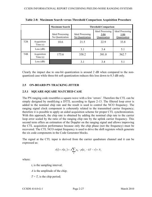
Table 2-8: Maximum Search versus Threshold Comparison Acquisition Procedure<br />
T2B Acquisition<br />
Time (s)<br />
T4B Acquisition<br />
Time (s)<br />
Maximum Search Threshold Comparison<br />
Ideal Processing<br />
No Quantization<br />
Ideal Processing<br />
No Quantization<br />
Ideal Processing<br />
3-bit<br />
Quantization<br />
Ideal Processing<br />
1-bit<br />
Quantization<br />
10.6 21.5 22.9 33.8<br />
Loss (dB) 3.1 3.4 5.1<br />
175.6 358.2 381.0 562.7<br />
Loss (dB) 3.1 3.4 5.1<br />
Clearly the impact due to one-bit quantization is around 2 dB when compared to the non-<br />
quantized case while three-bit soft quantization reduces this loss down to 0.3 dB only.<br />
2.5 ON-BOARD <strong>PN</strong> TRACKING JITTER<br />
2.5.1 SQUARE-SQUARE MATCHED CASE<br />
The <strong>PN</strong> ranging code resembles a square-wave with a few ‘errors’. Therefore the CTL can be<br />
simply designed by modifying a DTTL according to figure 2-13. The filtered loop error is<br />
added to the nominal chip rate and the result is used to control the NCO frequency. The<br />
ranging signal clock component is coherently related to the transmitted carrier frequency;<br />
therefore it is possible to apply an aided acquisition scheme for proper CTL synchronization.<br />
With this approach, the chip rate is obtained by adding the nominal chip rate to the carrier<br />
loop error scaled by the ratio of the ranging chip rate by the uplink carrier frequency. This<br />
second term offers an estimation of the Doppler on the ranging signal and allows improving<br />
the CTL acquisition performance because only the chip phase (not the frequency) must be<br />
recovered. The CTL NCO output frequency is used to drive the shift registers which generate<br />
the six code components in the Code Generator blocks.<br />
The signal at the CTL input is derived from the carrier quadrature channel and it can be<br />
expressed as:<br />
where:<br />
ts is the sampling interval;<br />
A is the amplitude of the chip;<br />
T = Tc is the chip period;<br />
() i = r(<br />
its<br />
) = A∑<br />
ak<br />
⋅ p(<br />
its<br />
− kT −τ<br />
) Ni<br />
r +<br />
k<br />
<strong>CCSDS</strong> 414.0-G-1 Page 2-27 March 2010