

elektronika electronics - Electronics Journal - Elektrotehnicki fakultet
elektronika electronics - Electronics Journal - Elektrotehnicki fakultet
elektronika electronics - Electronics Journal - Elektrotehnicki fakultet

You also want an ePaper? Increase the reach of your titles
YUMPU automatically turns print PDFs into web optimized ePapers that Google loves.
16<br />
R[ohm]<br />
6<br />
4<br />
2<br />
0<br />
0 1 2 3 4 5 6<br />
Frequency[GHz]<br />
Fig.3 Frequency dependence of parasitic resistances<br />
The intrinsic elements of the small signal equivalent<br />
model have been extracted at several bias conditions. The behavior<br />
of the tranconductance gm at 56 bias points is reported<br />
in Fig. 5 for a 900µm gate width device.<br />
Fig.4 Frequency dependence of parasitic capacitances<br />
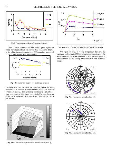
The consistency of the extracted elements values has been<br />
evaluated as a function of either the bias conditions and the<br />
device dimensions. Both extrinsic ed intrinsic elements depend<br />
on the gate width. As an example, in Fig 6 the behavior<br />
of the transconductance is reported and clear scaling effects<br />
can be seen.<br />
gm [S]<br />
C[pf]<br />
0.12<br />
0.08<br />
0.04<br />
0<br />
0 1 2 3 4 5 6<br />
VDS [V]<br />
Frequency[GHz]<br />
ELECTRONICS, VOL. 8, NO.1, MAY 2004.<br />
VGS [V]<br />
CPG<br />
CPD<br />
Rg<br />
Rs<br />
Rd<br />
Fig.5 Bias conditions dependence of the transconductance g m<br />
gm[S]<br />
0.6<br />
0.4<br />
0.2<br />
0<br />
0 2 4 6<br />
VDS<br />
W=300<br />
W=600<br />
W=900<br />
VGS=0V<br />
Fig.6 Behavior of g m vs. V ds for devices of scaled gate widths<br />
We report in Figs. 7-10 the comparison between the<br />
measured and simulated [S] parameters sets, as outputs of the<br />
AWR software, for a 900 µm device. This test thus gives a<br />
demonstration of the fitting performance of the extracted<br />
model.<br />
0<br />
0 .2<br />
-0.2<br />
0.4<br />
0.2<br />
-0.4<br />
0.6<br />
-0.6<br />
0.4<br />
0.8<br />
0.6<br />
-0.8<br />
0.8<br />
S11<br />
1.0<br />
1.0<br />
-1 .0<br />
2.0<br />
3.0<br />
-2.0<br />
2.0<br />
4.0<br />
5.0<br />
-3.0<br />
Swp Max<br />
6GHz<br />
3.0<br />
10 .0<br />
4.0<br />
-4 .0<br />
5.0<br />
10 .0<br />
-10.0<br />
-5.0<br />
Swp Min<br />
0.3475GHz<br />
Fig. 7 S 11 parameter measured and modeled<br />
Ma g Ma x<br />
25<br />
16 5<br />
-180<br />
150<br />
-16 5<br />
5<br />
Per Div<br />
-15 0<br />
13 5<br />
-135<br />
120<br />
-120<br />
105<br />
-105<br />
S21<br />
90<br />
-90<br />
75<br />
-75<br />
60<br />
-60<br />
45<br />
-45<br />
Swp Ma x<br />
6 GHz<br />
30<br />
-30<br />
1 5<br />
-1 5<br />
0<br />
Swp Min<br />
0.3475 GHz<br />
Fig. 8 S 21 parameter measured and modeled