

elektronika electronics - Electronics Journal - Elektrotehnicki fakultet
elektronika electronics - Electronics Journal - Elektrotehnicki fakultet
elektronika electronics - Electronics Journal - Elektrotehnicki fakultet

Create successful ePaper yourself
Turn your PDF publications into a flip-book with our unique Google optimized e-Paper software.
elations (16) and (17) given in the paper [3], where are<br />
U = U<br />
k r k<br />
2T<br />
, 2 2T<br />
r<br />
Z = Z<br />
k<br />
22<br />
k<br />
2T<br />
and .<br />
The obtained voltage vector is<br />
U S 1<br />
U S L<br />
Z S 1<br />
Z S L<br />
U S<br />
1<br />
L<br />
k 1<br />
2 T<br />
[<br />
+<br />
U = U | U<br />
Network<br />
1<br />
1<br />
L<br />
k+<br />
1<br />
2T<br />
, 1m<br />
1<br />
L<br />
ELECTRONICS, VOL. 8, NO.1, MAY 2004. 35<br />
]<br />
k+<br />
1 T<br />
2T<br />
, nL<br />
Network<br />
k<br />
. (22)<br />
1<br />
L<br />
1<br />
m+<br />
1<br />
n −1<br />
L<br />
Network<br />
1<br />
k+ 1<br />
Network<br />
2<br />
k+ 1<br />
st<br />
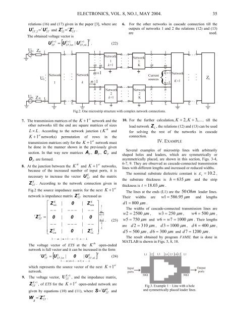
7. The transmission matrices of the K + 1 network and the<br />
other networks till the end are square matrices of sizes<br />
th<br />
L × L . According to the network junction ( K and<br />
st<br />
K + 1 networks) permutation of rows in the<br />
st<br />
transmission matrices only for the K + 1 network must<br />
be done in the manner shown in the previously given<br />
section. In that way new matrices , , and<br />
DP<br />
are formed.<br />
6. For the other networks in cascade connection till the<br />
outputs of networks 1 and 2 the relations (12) and (13)<br />
are used.<br />
Network<br />
1<br />
k+ K1<br />
Network<br />
2<br />
K<br />
1<br />
Current<br />
sources<br />
Fig.2. One microstrip structure with complex network connections.<br />
AP P B P C<br />
th<br />
st<br />
8. At the junction between the K and K + 1 networks,<br />
because of the increased number of input ports, it is<br />
K<br />
2T<br />
necessary to increase the vector and the matrix<br />
K<br />
Z2T<br />
. According to the network connection given in<br />
Fig.2 the source impedance matrix for the next<br />
K<br />
2T<br />
network is impedance matrix increased as<br />
i<br />
Z<br />
K<br />
2T<br />
K<br />
⎡ ZmL<br />
⎢<br />
⎢<br />
− −<br />
= ⎢ 0<br />
⎢<br />
⎢ − −<br />
⎢ K<br />
⎣ Z Lm<br />
|<br />
|<br />
|<br />
|<br />
|<br />
0<br />
Z<br />
− − −<br />
0<br />
− − −<br />
0<br />
|<br />
|<br />
|<br />
|<br />
|<br />
U<br />
Z<br />
1 � m | m + 1�<br />
n − 1|<br />
n � L<br />
K<br />
mm<br />
− −<br />
− −<br />
Z<br />
0<br />
K<br />
LL<br />
⎤<br />
⎥<br />
⎥<br />
⎥<br />
⎥<br />
⎥<br />
⎥<br />
⎦<br />
1<br />
1<br />
1<br />
�<br />
m<br />
m+<br />
�<br />
n−<br />
n<br />
�<br />
L<br />
st<br />
K + 1<br />
. (23)<br />
The voltage vector of ETS at the<br />
th<br />
K open-ended<br />
network is full vector and it can be increased in the form<br />
i<br />
U<br />
K<br />
2 T<br />
k<br />
k<br />
[ U | 0 | ]<br />
= U<br />
2T<br />
, 1m<br />
2T<br />
, nL<br />
1 � m | m+<br />
1�<br />
n-1<br />
| n � L<br />
T<br />
(24)<br />
st<br />
K + 1<br />
which represents the source vector of the next<br />
network.<br />
K + 1<br />
9. The voltage vector, U , and the impedance matrix,<br />
Z<br />
K+<br />
1<br />
2T<br />
, of ETS for the<br />
2T<br />
st<br />
K + 1 open-ended network are<br />
given by equations (10) and (11), where and<br />
i<br />
W = Z<br />
s<br />
K<br />
2T<br />
.<br />
i<br />
S= U<br />
K<br />
2T<br />
L<br />
1<br />
m + 1<br />
n − 1<br />
L<br />
Network<br />
K+ 1<br />
10. For the further calculation, K + 2 , K + 3,...<br />
, till the<br />
Z<br />
1<br />
L<br />
1<br />
L<br />
ZL<br />
load network L , the relations (12) and (13) can be used<br />
for solving the rest of the networks in cascade<br />
connection.<br />
IV. EXAMPLE<br />
Several examples of microstrip lines with arbitrarily<br />
shaped holes and leaders, which are symmetrically or<br />
asymmetrically placed, are shown in this section, Figs. 3-4,<br />
6-7, 9. They are observed as cascade-connected transmission<br />
lines with different lengths and increased or reduced widths.<br />
The nominal substrate dielectric constant is ε r = 10.<br />
2 ,<br />
the substrate thickness is h = 635 µ m and the strip<br />
thickness is t = 18.<br />
03 µ m .<br />
50Ohm<br />
The lines at the ends (L1) are the leader lines.<br />
Their widths are w 1 = 586.<br />
95 µ m and lengths<br />
d 1 = 800 µ m .<br />
The widths of cascade-connected transmission lines are<br />
w 2 = 2500 µ m , w 3 = 250 µ m , w 4 = 500 µ m ,<br />
w 5 = 750 µ m and w 6 = w7<br />
= 1000 µ m . Their lengths<br />
are d 2 = 310 µ m , d 3 = 1000 µ m , d 4 = 400 µ m ,<br />
d 5 = 500 µ m , d 6 = 300 µ m and d 7 = 1200 µ m .<br />
The result obtained by program FAMIL that is done in<br />
MATLAB is shown in Figs. 5, 8, 10.<br />
Input<br />
ports<br />
L1 L2 L3 L4 L5 L6 L2 L1<br />
50Ω 50 Ω<br />
Fig.3. Example 1 – Line with a hole<br />
and symmetrically placed leader lines.<br />
Output<br />
ports