

elektronika electronics - Electronics Journal - Elektrotehnicki fakultet
elektronika electronics - Electronics Journal - Elektrotehnicki fakultet
elektronika electronics - Electronics Journal - Elektrotehnicki fakultet

You also want an ePaper? Increase the reach of your titles
YUMPU automatically turns print PDFs into web optimized ePapers that Google loves.
26<br />
ELECTRONICS, VOL. 8, NO.1, MAY 2004.<br />
Self-Heating Effects in Virtual Substrate SiGe HBTs<br />
Abstract - In this paper we investigated the self-heating<br />
effects in SiGe heterojunction bipolar transistors (HBTs)<br />
fabricated on SiGe alloy virtual substrate. Using a twodimensional<br />
process and device numerical simulation, we have<br />
found that self-heating effects and local temperature increase<br />
due to the internal power dissipation are substantially more<br />
pronounced in virtual substrate HBTs in comparison with<br />
identical HBT devices on silicon substrate.<br />
Keywords - HBT, virtual, substrate, self-heating<br />
I INTRODUCTION<br />
Modern Silicon Heterojunction Bipolar Transistors (Si<br />
HBTs) with strained-SiGe base are very promising devices<br />
for high-frequency circuit applications [1]. The ECL<br />
microwave circuits in SiGe HBT/CMOS technology has already<br />
achieved fmax>180-GHz [2]. Recently, a new type of so-called<br />
“virtual substrate” technology [3] is emerging that allows a<br />
fabrication of both the high-performance heterojunction MOS<br />
FETs (HFETs) and SiGe HBTs on the same chip. The virtual<br />
substrate (VS) consists of thick (1um) fully relaxed SiGe<br />
buffer layer epitaxially grown on silicon substrate. The ability<br />
to synthesize on-chip HFETs, inductors and microstrip<br />
structures together with HBTs on VS makes SiGe HBTs ideal<br />
for microwave and RF applications [4]. There is no<br />
fundamental difference in the operation between Si HBTs<br />
and virtual substrate HBTs (VS HBTs) [5]. However, the<br />
thermal conductivity of the SiGe alloy forming the virtual<br />
substrate layer is much lower (approximately 15x lower at<br />
20% Ge composition( then that of silicon [6].<br />
Thus, during the DC operation of the device, VS HBT<br />
experiences considerably more self-heating than conventional<br />
Si HBT. Lattice self-heating results from the high dissipated<br />
power density in the device. Even in low-power-applications,<br />
the scaled sub-micron VS HBTs operating at high collector<br />
current densities for maximum speed experience a nonnegligible<br />
self-heating effects. A local increase of device<br />
temperature degrades VS HBT performance by reducing its<br />
cutoff frequencies ft and fmax and increasing internal leakage<br />
currents . Self-heating of HBTs can also significantly affects<br />
the behaviour of precision analog circuits, such as current<br />
sources and current mirrors, by changing their output<br />
admittances and introducing errors due to the increased<br />
device mismatching [7,8].<br />
1 Micro<strong>electronics</strong> Department, Faculty of Electronic<br />
Engineering Nis, Universityof Nis, Beogradska 14, 18000 Nis,<br />
Serbia and Montenegro. E-mail:janko@elfak.ni.ac.yu<br />
2 School of Electrical, Electronic and Computer Engineering,<br />
Merz Court, University of Newcastle, NE1 7RU, United Kingdom,<br />
E-mail: A.B.Horsfall @newcastle.ac.uk<br />
Nebojsa D. Jankovic 1 , Aulton B. Horsfall 2<br />
In this paper, we will evaluate the self-heating effects in<br />
VS HBTs by using a commercial numerical technology and<br />
device simulation software (TCAD) from SILVACO [9]. For<br />
accurate prediction of the self-heating in sub-micron devices,<br />
it is necessary to employ a full energy balance and thermionic<br />
emission models thath are connected with appropriate<br />
thermal models in simulations. It is achieved using<br />
SILVACO (GIGA) software package [9], which solves selfconsistently<br />
the electro-thermal coupled transport equations.<br />
A comparison between self-heating effects occurring in Si<br />
HBT and VS HBT at the similar DC power dissipation will<br />
be performed with respect to the VS HBT’s output<br />
impedance, and current gain.<br />
II 2D DEVICE STRUCTURE AND NUMERICAL<br />
MODELLING<br />
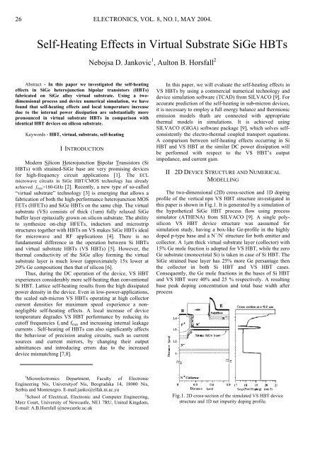
The two-dimensional (2D) cross-section and 1D doping<br />
profile of the vertical npn VS HBT structure investigated in<br />
this paper is shown in Fig.1. It is generated by a simulation of<br />
the hypothetical SiGe HBT process flow using process<br />
simulator (ATHENA) from SILVACO [9]. A single polysilicon<br />
VS HBT device structure was aassumed for<br />
simulation study, having a box-like Ge-profile in the highly<br />
doped p-type base and a N + /N - structure for both emitter and<br />
collector. A 1µm thick virtual substrate layer (collector) with<br />
15% Ge mole fraction is adopted for VS HBT, while the zero<br />
Ge substrate (monocristal Si) is taken in case of Si HBT. The<br />
SiGe strained base layer has 25% more Ge persantage then<br />
the collector in both Si HBT and VS HBT cases.<br />
Consequently, the Ge mole fractions in the bases of Si HBT<br />
and VS HBT were 40% and 25 % respectively. A resulting<br />
base peak doping concentration and total base width after<br />
process<br />
Fig.1. 2D cross-section of the simulated VS HBT device<br />
structure and 1D net impurity doping profile.