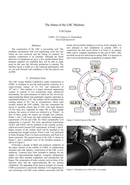
- Page 18 and 19: II. THE LATTICE The main parameters
- Page 20 and 21: two companies, and the first one ha
- Page 22 and 23: Trends and Challenges in High Speed
- Page 24 and 25: Figure 5: Trends in Power Consumpti
- Page 26 and 27: compromise between the required tim
- Page 28 and 29: IN C in L.F. Feedback Preamp Shaper
- Page 30 and 31: [21] G.Anelli, "Design and characte
- Page 32 and 33: ECAL HCAL SPD PreShower clip PM cli
- Page 34 and 35: Test Pulse Test Pulse SPLITTER INTE
- Page 36 and 37: C d Cryostat Motherboard Electrode
- Page 38 and 39: 1 ⁄ gm1 RC1 ZIN = ---------------
- Page 40 and 41: Many of the earlier families are st
- Page 42 and 43: The future solution is bit-serial s
- Page 44 and 45: D. Designing for Radiation Toleranc
- Page 46 and 47: Single Event Upset Tests of Commerc
- Page 48 and 49: V. SRAM FPGA TECHNOLOGY The Xilinx
- Page 50 and 51: at read out (corrected before read
- Page 52 and 53:
IX SINGLE EVENT TRANSIENTS In addit
- Page 54 and 55:
Electronics Commissioning Experienc
- Page 56 and 57:
CHAMBER HV BOARD GAS BOX HV 00 11 0
- Page 58 and 59:
The maximum bandwidth of the Switch
- Page 60 and 61:
The EndCap will communicate with th
- Page 62 and 63:
B. Power supply The power supply ha
- Page 64 and 65:
È�Ö�ÓÖÑ�Ò � Ó� Ø
- Page 66 and 67:
Analogue Input Pads Protection Diod
- Page 68 and 69:
data header DataValid 128 channels
- Page 70 and 71:
�ÜÔ� Ø�� �ÖÓÑ ×�
- Page 72 and 73:
PRELIMINARY ���ÙÖ� ��
- Page 74 and 75:
Development of a High Density Pixel
- Page 76 and 77:
power pad interfaces of FPIX1 exten
- Page 78 and 79:
[mm] Readout chip Pixel Sensor Figu
- Page 80 and 81:
B. Registers in preFPIX2Tb readout
- Page 82 and 83:
The high beam fluence used during t
- Page 84 and 85:
• provide an interface between th
- Page 86 and 87:
Figure 6: A snapshot of DAQ Monitor
- Page 88 and 89:
The HAL25 Front-End Chip for the AL
- Page 90 and 91:
The signal is sampled on the storag
- Page 92 and 93:
Fig. 9 Output stream Figure 10 show
- Page 94 and 95:
II. The front−end ASICs The front
- Page 96 and 97:
espectively. These numbers fulfill
- Page 98 and 99:
to thin the pixel chip wafers, afte
- Page 100 and 101:
After the irradiation the output vo
- Page 102 and 103:
Progress in Development of the Anal
- Page 104 and 105:
this signal distribution, assuming
- Page 106 and 107:
SCTA128VG chip before and after irr
- Page 108 and 109:
out by one PILOT multi chip module
- Page 110 and 111:
III. PHYSICAL IMPLEMENTATION A. Pix
- Page 112 and 113:
http://www.semiconductor.agilent.co
- Page 114 and 115:
1. Indium Bumps: Occurrence A: A go
- Page 116 and 117:
Beamtests of Prototype ATLAS SCT Mo
- Page 118 and 119:
IV. MEASUREMENTS A total of over a
- Page 120 and 121:
K3112 front: residuals @ 1fC Chi2 /
- Page 122 and 123:
ealization in order to ensure a hig
- Page 124 and 125:
controlled by means of a standard V
- Page 126 and 127:
Radiation Tests on Commercial Instr
- Page 128 and 129:
FET-input instrumentation amplifier
- Page 130 and 131:
tron radiation (Figure 9). A change
- Page 132 and 133:
II. TESTING PLAN Four experiments h
- Page 134 and 135:
The results show that the figures f
- Page 136 and 137:
Use of antifuse-FPGAs in the Track-
- Page 138 and 139:
Figure 3(a) shows the JTAG net thro
- Page 140 and 141:
procedure established in [5], we ca
- Page 142 and 143:
The optical and opto-electronic com
- Page 144 and 145:
Current (mA) 6 5 4 3 2 1 0 0.00E+00
- Page 146 and 147:
Radiation test and application of F
- Page 148 and 149:
Two devices were programmed with th
- Page 150 and 151:
VI. THE FPGA SUBSYSTEM. After the r
- Page 152 and 153:
(“dav” and “cav”). Dependin
- Page 154 and 155:
3) Commercial Serializer Using a tr
- Page 156 and 157:
Development of an Optical Front-end
- Page 158 and 159:
een proven to be very robust in ter
- Page 160 and 161:
The short broadcast port of the TTC
- Page 162 and 163:
The channels can be individually ad
- Page 164 and 165:
B. Dynamic performance The dynamic
- Page 166 and 167:
Quality Assurance Programme for the
- Page 168 and 169:
The advance validation procedure is
- Page 170 and 171:
(i) Laser AVT. At least 20 lasers w
- Page 172 and 173:
II. PRODUCTION FLOW In the producti
- Page 174 and 175:
4.0x10 -2 Equivalent Input Non Line
- Page 176 and 177:
Figure 1 SCT links architcture. III
- Page 178 and 179:
Figure 9 photograph of a forward SC
- Page 180 and 181:
Prototype Analogue Optohybrids for
- Page 182 and 183:
Crosstalk between channels on the p
- Page 184 and 185:
Link output (V) EINL (mV) EIN (mV)
- Page 186 and 187:
separate fibers for transmission an
- Page 188 and 189:
Development and a SEU Test of a TDC
- Page 190 and 191:
Idd[mA] Tpd[ns] 7 6 5 4 3 2 1 0 0.0
- Page 192 and 193:
σ SEU (CSR) < 5.6x10 -15 cm 2 /bit
- Page 194 and 195:
as minimise power consumption. Stan
- Page 196 and 197:
The chip was designed using the AMI
- Page 198 and 199:
Results of Radiation Tests of the A
- Page 200 and 201:
III. NEUTRON IRRADIATION OF THE ANO
- Page 202 and 203:
CMOS front-end for the MDT sub-dete
- Page 204 and 205:
III. TEST RESULTS The MDT-ASD has b
- Page 206 and 207:
All systematic charge measurement e
- Page 208 and 209:
acting as a high pass filter for th
- Page 210 and 211:
verify the dependence using counter
- Page 212 and 213:
Status of the CARIOCA Project W. Bo
- Page 214 and 215:
Figure 7: Schematic of the pole/zer
- Page 216 and 217:
TTCPR: A PMC Receiver for TTC John
- Page 218 and 219:
A PROTOTYPE FAST MULTIPLICITY DISCR
- Page 220 and 221:
In Figure 3 we present, as a functi
- Page 222 and 223:
Another experimental result is pres
- Page 224 and 225:
current TIM-0 modules : • To tran
- Page 226 and 227:
The CPLD devices used on TIM-0 ( Fi
- Page 228 and 229:
Abstract In this paper we describe
- Page 230 and 231:
IV. THE READOUT SUPERVISOR The Read
- Page 232 and 233:
throttle lines trigger the state of
- Page 234 and 235:
• MAX+plus II and AHDL were chose
- Page 236 and 237:
JTAG Interface from Glue Board TMS
- Page 238 and 239:
VIII. REFERENCES [1] R.Jacobsson, B
- Page 240 and 241:
The calorimeter regional crate syst
- Page 242 and 243:
The four highest energy central and
- Page 244 and 245:
The Track-Finding Processor for the
- Page 246 and 247:
the configuration time down to 6 se
- Page 248 and 249:
Latency 1 1 4 2 3 2 3 3 2 Clock and
- Page 250 and 251:
up to 7 high-p T pad logic boards a
- Page 252 and 253:
The output from the comparison bloc
- Page 254 and 255:
Abstract One Size Fits All: Multipl
- Page 256 and 257:
performance, either on the individu
- Page 258 and 259:
total jet-ET thresholds. This can n
- Page 260 and 261:
Calorimeter ~7200 anal. summed trig
- Page 262 and 263:
2.0 cm Figure 6: Partly assembled M
- Page 264 and 265:
Prototype Readout Module for the AT
- Page 266 and 267:
The implementation has the followin
- Page 268 and 269:
FIFOs, and remained asserted until
- Page 270 and 271:
Figure 2 shows the trigger scheme.
- Page 272 and 273:
B. PAD Logic boxes The first step o
- Page 274 and 275:
Fast Pre-Trigger Electronics of T0/
- Page 276 and 277:
D. Functions Centrality of collisio
- Page 278 and 279:
Results of in-beam tests at CERN of
- Page 280 and 281:
4 x 9 bit TRACO previews I/O pads T
- Page 282 and 283:
The behaviour of the TSS under radi
- Page 284 and 285:
NP4GS3 requires its own memories an
- Page 286 and 287:
The very high speed of the ingress
- Page 288 and 289:
Abstract STATUS OF ATLAS LAr DMILL
- Page 290 and 291:
The second stage is built around a
- Page 292 and 293:
3.3 Gain selector The SCA is follow
- Page 294 and 295:
DeltaStream : A 36 channel low nois
- Page 296 and 297:
e clk s Track/Hold Q pulse on input
- Page 298:
Measurement type & Low Gain High Ga
- Page 301 and 302:
¯ Û� ��Ú� ØÓ �Ö�
- Page 303 and 304:
in1 in1 in2 in2 clock+ clock− �
- Page 305 and 306:
Production and Test of the ATLAS Ha
- Page 307 and 308:
krad of ionizing radiation. 18 samp
- Page 309 and 310:
Low Voltage Control for the Liquid
- Page 311 and 312:
Figure 5: PVSS2 daughter panel “C
- Page 313 and 314:
5) Safety aspects Temperature senso
- Page 315 and 316:
leaving the complete analysis to th
- Page 317 and 318:
•Test of motherboard and PUs. Thi
- Page 319 and 320:
• Muon-RPC: 5 sources @ ~300 byte
- Page 321 and 322:
32 MB SDRAM Altera APEX PCI 64bits
- Page 323 and 324:
chopper stabilised amplifier, a dig
- Page 325 and 326:
temperature increase but then decre
- Page 327 and 328:
[4] CAN in Automation (CiA), D-9105
- Page 329 and 330:
applying selective readout and zero
- Page 331 and 332:
Vertical Slice of the ATLAS Detecto
- Page 333 and 334:
was easily extended in order to dri
- Page 335 and 336:
A rad-hard 8-channel 12-bit resolut
- Page 337 and 338:
Figure 5: DCU test-board block diag
- Page 340 and 341:
Design specifications and test of t
- Page 342 and 343:
Figure 2: DCS software architecture
- Page 344 and 345:
is active. If the transition is cro
- Page 346 and 347:
plexed. Each channel is then fed to
- Page 348 and 349:
parity checks on the PCI busses. Th
- Page 350 and 351:
either ground or another group of c
- Page 352 and 353:
y a linearized model around the equ
- Page 355 and 356:
! "# $ %& ''()*" $ % + (% % ,# - -
- Page 357 and 358:
2 &= . . - 7= . . , . " . 2 ! - . /
- Page 359 and 360:
- 3=
- Page 361 and 362:
Present requirements[2] for low vol
- Page 363 and 364:
I. 4−fold way Final design of the
- Page 366 and 367:
Conductive Cooling of SDD and SSD F
- Page 368 and 369:
Tx-Tin, deg.C �� �� ��
- Page 370 and 371:
Figure 6: Foto of the SDD detector
- Page 372 and 373:
clock, sorting “3 out of 18” an
- Page 374 and 375:
Table 3: Results of Simulation Muon
- Page 376 and 377:
I. DATA SERIALIZER AND OPTICAL MODU
- Page 378 and 379:
V. CONCLUSION Table 2: Measured SEU
- Page 380 and 381:
single-chip multiprocessors on N-le
- Page 382 and 383:
PCI-SCI Modular Bridge Chip (PSB) w
- Page 384 and 385:
6E can also be configured as a stan
- Page 386 and 387:
ICSNET/1993,S-Petersburg .http://el
- Page 388 and 389:
�¨�¨��§�����
- Page 390 and 391:
�����������
- Page 392 and 393:
Studies for a Detector Control Syst
- Page 394 and 395:
For redundancy and grounding consid
- Page 396 and 397:
to send test signals to the interlo
- Page 398 and 399:
CADENCE's SPECCTRAQuest TM SI exper
- Page 400 and 401:
• package impedance effects. DC t
- Page 402 and 403:
Influence of Temperature on Pulsed
- Page 404 and 405:
collected charge temperature depend
- Page 406 and 407:
Figure 3: Potential distributions a
- Page 408 and 409:
Estimating induced-activation of SC
- Page 410 and 411:
esulting in a p-p interaction rate
- Page 412 and 413:
(a) 1.50m r 0 r Figure 2: Considere
- Page 414 and 415:
Development of a DMILL radhard mult
- Page 416 and 417:
lock onto, and a ’single error fl
- Page 418 and 419:
Direct Study of Neutron Induced Sin
- Page 420 and 421:
THE ATLAS READ OUT DATA FLOW CONTRO
- Page 422 and 423:
1. Input monitoring, masking, stimu
- Page 424 and 425:
REFERENCES [1] P. Gällnö:"Timing,
- Page 426 and 427:
Figure 3: VCSEL power. Power output
- Page 428 and 429:
An Emulator of Timing, Trigger and
- Page 430 and 431:
have two kinds of the reset signal,
- Page 432 and 433:
��Ö×Ø �ÓÑÑ�××�Ó
- Page 434 and 435:
� Ñ��Ð �ÓÜ ÔÖÓØÓ
- Page 436 and 437:
HIGH-SPEED MULTICHANNEL ICs FOR FRO
- Page 438 and 439:
Parameters of ECL D-trigger Name of
- Page 440 and 441:
References 1. E.Atkin, Yu.Volkov, S
- Page 442 and 443:
The LDO can deliver to the load a m
- Page 444:
options are available in the DAC. E