preliminary - Bad Request - Cern
preliminary - Bad Request - Cern
preliminary - Bad Request - Cern

Create successful ePaper yourself
Turn your PDF publications into a flip-book with our unique Google optimized e-Paper software.
B. Designing for Signal Integrity<br />
Signal Integrity refers to signal quality on the PC-board,<br />
where it is important to avoiding reflections which show up<br />
as ringing, resulting in erroneous clocking or even data dropout.<br />
The user should develop a good understanding of<br />
transmission-line effects, and the various methods to<br />
terminate the lines.<br />
The controlled-impedance output drivers, available on all<br />
Virtex-II outputs, are a big help.<br />
Power supply decoupling is becoming more and more<br />
important. In CMOS circuits, power-supply current is<br />
predominantly dynamic. In a single-clock synchronous<br />
system, there is a supply-current spike during each active<br />
clock edge, but no current in-between. This dynamic current<br />
can be many times the measured dc value, and these current<br />
spikes cannot possibly be supplied from the far-away power<br />
supply. They must come from the local decoupling<br />
capacitors. The rule is: attach one 0.01 to 0.1 uF very closely<br />
to each Vcc pin, and tie them directly to the ground plane.<br />
The capacitance is not critical, low resistance and inductance<br />
are far more important. Two capacitors in parallel are much<br />
better than one large capacitor.<br />
Model the PC-board behavior with HyperLynx. Multilayer<br />
PC-boards with uninterrupted ground- and Vcc planes<br />
are a must, as is the controlled-impedance routing of clock<br />
lines.<br />
1) Tricks of the Trade<br />
To improve signal integrity, reduce output strength. Both<br />
LVTTL and LVCMOS have options for 2, 4, 6, 8, 12, 16, and<br />
24mA sink and source current. Controlled-impedance outputs<br />
(series-termination) is even better, but watch out for loads<br />
that are distributed along the line. They will see a staircase<br />
voltage, which will cause severe problems.<br />
Explore different supply voltages and I/O standards.<br />
Optimize drive capability and input threshold for the task at<br />
hand. Use differential signaling, e.g. LVDS when necessary.<br />
Avoid unnecessary fan-out, load capacitance and trace length.<br />
To combat Simultaneously Switching Output (SSO)<br />
problems causing ground-bounce, add virtual ground pins:<br />
High sink-current output pins that are internally and<br />
externally connected to ground.<br />
2). Test for Performance and Reliability<br />
You can manipulate the IC speed while it sits on the<br />
board:<br />
High temperature and low Vcc = slow operation,<br />
Low temperature and high Vcc = fast operation.<br />
If operation fails at hot, the circuit is not fast enough.<br />
Check the design for speed bottlenecks, add pipeline stages,<br />
or buy a faster speed-grade device.<br />
If operation fails at cold, the circuit is too fast. Check the<br />
design for signal integrity and hold-time issues, check for<br />
clock reflections. Look for internal clock delays causing<br />
hold-time issues, look for “dirty asynchronous tricks” inside<br />
the chip, like decoders driving clocks. In short, if it fails cold,<br />
there is something wrong with the design, not with the<br />
device.<br />
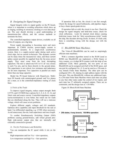
C. BlockROM State Machines.<br />
The Virtex-II BlockROMs can be used as surprisingly<br />
efficient state machines.<br />
With a common algorithm stored in the RAM (used as<br />
ROM) one BlockRAM can implement a 20-bit binary or<br />
Grey counter, or a 6-digit BCD counter (with the help of one<br />
additional CLB). More generally, the two ports of one<br />
BlockRAM can be assigned each half of the RAM space, and<br />
one port be configured 1k x 9. It can be used as a 256-state 4way<br />
branch Finite State Machine. The other port can be<br />
configured 256 x 36, sharing its eight address inputs with the<br />
first port. This one BlockRAM, without any additional logic,<br />
is a 256-state Finite State Machine where each state can jump<br />
to any four other states under the control of two inputs, and<br />
each state has 37 arbitrarily assigned outputs. There are no<br />
constraints, and the design runs at >150 MHz.<br />
Figure 10: Block RAM State Machine<br />
Branch<br />
8 bits<br />
BlockROM<br />
1K x 9<br />
8 + 1 bits<br />
Control bits<br />
Unused<br />
Output<br />
M 256 states, 4-way branch, 150 MHz operation<br />
Branch<br />
Control 2 bits<br />
Block ROM<br />
1K x 9<br />
8 bits 8 + 1 bits<br />
8 bits 256 x 36<br />
36 bits<br />
M 36 additional parallel outputs<br />
Output