

VHDL Made Easy! - Xilinx
VHDL Made Easy! - Xilinx
VHDL Made Easy! - Xilinx
- TAGS
- vhdl
- xilinx
- www.xilinx.com

You also want an ePaper? Increase the reach of your titles
YUMPU automatically turns print PDFs into web optimized ePapers that Google loves.
36<br />
Structured Floorplanning for the XC8100:<br />
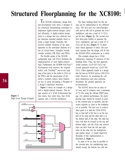
Figure 1<br />
High Level Design Example<br />
The XC8100 architecture, design flow<br />
and development tools allow a designer to<br />
use structured floorplanning techniques to<br />
implement highly-ordered designs easily<br />
and efficiently. A highly-ordered design<br />
refers to a design that uses relatively simple<br />
functions repeated multiple times to<br />
create a larger design. Typically, this<br />
involves multiple iterations of the same<br />
operation on the individual elements of a<br />
bus or several buses. Examples include<br />
crossbar switches, FIR filters and FIFOs.<br />
The flexible nature of the XC8100<br />
configurable logic cell (CLC) facilitates the<br />
implementation of such highly-ordered<br />
logic. Furthermore, the XC8000 XACTstep TM<br />
development tools preserve the original<br />
netlist, with TrueMap TM one-to-one mapping<br />
of the gates in the netlist to CLCs in<br />
the FPGA and the preservation of the<br />
netlist’s symbolic names; these features<br />
are key to easily developing a floorplan of<br />
a design’s repetitious structures.<br />
Figure 1 shows an example of a design<br />
with a highly-ordered structure. This design<br />
consists of a 32-bit bi-directional bus,<br />
four clocks, four select lines, four 32-bit<br />
registers and a 32x4-bit mulitplexer.<br />
The basic building block for this design<br />
can be implemented in two different<br />
ways. The first uses two sum-of-product<br />
cells and an OR cell to generate the 4-to-1<br />
multiplexer, and uses a total of 11 CLCs<br />
per bit slice (Figure 2). The second uses<br />
four three-state buffers to generate the<br />
4-to-1 multiplexer, and uses a total of 12<br />
CLCs per bit slice (Figure 3). To determine<br />
which approach is better, the user<br />
must examine how the design will fit into<br />
the XC8100 FPGA architecture as a whole.<br />
This example design has a 32-bit<br />
architecture, requiring 32 instances of this<br />
building block. Thus, the first approach<br />
would consume 11x32=352 CLCs; the<br />
second approach would use 12x32=384<br />
CLCs. Either approach results in a design<br />
that fits into an XC8101 devices (384 CLCs<br />
total). However, by examining the cell<br />
array dimensions and some potential<br />
floorplans, the optimal approach can<br />
be determined.<br />
The XC8101 device has an array of<br />
16 rows and 24 columns, with a maximum<br />
of 72 I/Os using the 100-pin PQFP package.<br />
For optimal performance, the multiplexing<br />
logic should be located as close<br />
to the external pins as possible, and the<br />
source registers as close to the multiplexers<br />
as possible. The best way to achieve<br />
these goals is to split the 32-bit DATA<br />
bus so that half of the bus is on the top<br />
half of the chip and the other half is in<br />
the bottom half of the chip. The data bus<br />
lines will then be located on the top and<br />
bottom edges, and the clock and selector<br />
lines can drive from the left and right<br />
sides of the chip into the multiplexers<br />
and register arrays. A simple high-level<br />
floorplan of this implementation is<br />
illustrated in Figure 4.<br />
In order to be as close as possible to<br />
the external pins, the multiplexing logic<br />
should occupy the bottom two and top


