

VHDL Made Easy! - Xilinx
VHDL Made Easy! - Xilinx
VHDL Made Easy! - Xilinx
- TAGS
- vhdl
- xilinx
- www.xilinx.com

Create successful ePaper yourself
Turn your PDF publications into a flip-book with our unique Google optimized e-Paper software.
38<br />
Structured<br />
Floorplanning<br />
Continued from the previous page<br />
Figure 5<br />
Multiplexer<br />
Floorplan<br />
Layout 1, 2<br />
bus bits<br />
Figure 6<br />
Multiplexer<br />
Floorplan<br />
Layout 2, 2<br />
bus bits<br />
knowledge of the design’s structure, a<br />
truly optimized design can be achieved.<br />
Figures 5 and 6 show two possible<br />
floorplans for the multiplexer logic; where<br />
bb_0 refers to the DATA bus bit 0 building<br />
block, bb_1 refers to the DATA bus<br />
bit 1 building block, and sop_0, sop_1<br />
and or_0 refer to the combinatorial logic<br />
shown in Figure 2. Both of these layouts<br />
work reasonably well; they are small and<br />
fit evenly into the allotted 2x24 CLC area.<br />
The second layout has a slight advantage<br />
in that the nets from the sop_0 and sop_1<br />
instances to the or_0 instance will be of<br />
equal length; thus, this floorplan will be<br />
adopted.<br />
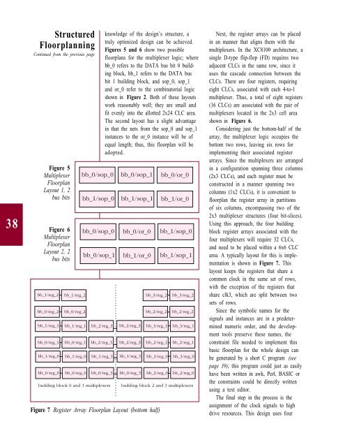
Figure 7 Register Array Floorplan Layout (bottom half)<br />
Next, the register arrays can be placed<br />
in an manner that aligns them with the<br />
multiplexers. In the XC8100 architecture, a<br />
single D-type flip-flop (FD) requires two<br />
adjacent CLCs in the same row, since it<br />
uses the cascade connection between the<br />
CLCs. There are four registers, requiring<br />
eight CLCs, associated with each 4-to-1<br />
multiplexer. Thus, a total of eight registers<br />
(16 CLCs) are associated with the pair of<br />
multiplexers located in the 2x3 cell area<br />
shown in Figure 6.<br />
Considering just the bottom-half of the<br />
array, the multiplexer logic occupies the<br />
bottom two rows, leaving six rows for<br />
implementing their associated register<br />
arrays. Since the multiplexers are arranged<br />
in a configuration spanning three columns<br />
(2x3 CLCs), and each register must be<br />
constructed in a manner spanning two<br />
columns (1x2 CLCs), it is convenient to<br />
floorplan the register array in partitions<br />
of six columns, encompassing two of the<br />
2x3 multiplexer structures (four bit-slices).<br />
Using this approach, the four building<br />
block register arrays associated with the<br />
four multiplexers will require 32 CLCs,<br />
and need to be placed within a 6x6 CLC<br />
area. A typically layout for this is implementation<br />
is shown in Figure 7. This<br />
layout keeps the registers that share a<br />
common clock in the same set of rows,<br />
with the exception of the registers that<br />
share clk3, which are split between two<br />
sets of rows.<br />
Since the symbolic names for the<br />
signals and instances are in a predetermined<br />
numeric order, and the development<br />
tools preserve these names, the<br />
constraint file needed to implement this<br />
basic floorplan for the whole design can<br />
be generated by a short C program (see<br />
page 39); this program could just as easily<br />
have been written in awk, Perl, BASIC or<br />
the constraints could be directly written<br />
using a text editor.<br />
The final step in the process is the<br />
assignment of the clock signals to high<br />
drive resources. This design uses four


