Huge Images? - GIT Verlag
Huge Images? - GIT Verlag
Huge Images? - GIT Verlag

Create successful ePaper yourself
Turn your PDF publications into a flip-book with our unique Google optimized e-Paper software.
69721<br />
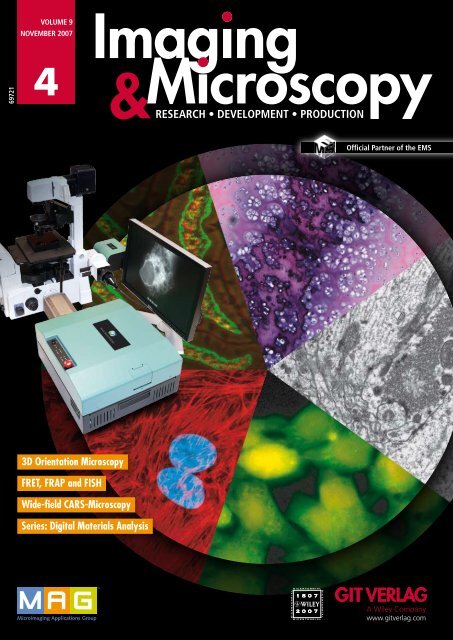
VOLUME 9<br />
NOVEMbER 2007<br />
4<br />
3D Orientation Microscopy<br />
FRET, FRAP and FISH<br />
Wide-field CARS-Microscopy<br />
Series: Digital Materials Analysis<br />
Imaging<br />
Microscopy<br />
&RESEARCH • DEVELOPMENT • PRODUCTION<br />
Official Partner of the EMS<br />
G.I.T. Imaging www.gitverlag.com<br />
& Microscopy 2/2007 •
A New Age of Vision:<br />
Superresolution Microscopy!<br />
New concepts in microscopy revolutionize biomedical research<br />
Our new 4Pi and STED microscopy systems provide research scientists with the tools they need<br />
to find answers to many of life’s unresolved questions. With their superb resolving power,<br />
these progressive microscopy technologies break through the physical barriers of visibility, enabling<br />
the exploration of completely new perspectives in biomedicine.<br />
www.leica-microsystems.com/Confocal_Microscopes<br />
z<br />
Confocal x<br />
4Pi<br />
x<br />
Confocal y<br />
STED
Nobel Prize for Surface Scientist Gerhard Ertl<br />
Dear Reader,<br />
Some days ago the Royal Swedish Academy<br />
of Sciences announced the 2007 Nobel<br />
Prize in Chemistry for Gerhard Ertl,<br />
professor emeritus at the Fritz-Haber Institute<br />
in Berlin.<br />
Imaging & Microscopy congratulates<br />
Gerhard Ertl for this most prestigious<br />
honour in science that is awarded due to<br />
his thorough studies of chemical reactions<br />
on solid surfaces. When having a<br />
closer look on fundamental molecular<br />
processes at the gas-solid interface, small<br />
gas molecules may either be adsorbed or<br />
bounce back at the solid surface, according<br />
to a note by the Royal Swedish Academy<br />
of Sciences (www.kva.se). The first<br />
case includes the most interesting possibilities:<br />
The gas molecule can dissociate<br />
at the interface, the chemical properties<br />
of the surface can be changed, or the absorbed<br />
molecule can chemically react<br />
with a previously absorbed one.<br />
Ertl’s giant step forward in the understanding<br />
of these scenarios led to various<br />
breakthroughs in the development of catalysts<br />
being invaluable across industry.<br />
Carbon monoxide and hydrocarbons are<br />
converted to carbon dioxide in vehicles<br />
exhaust gasses today, and even the content<br />
of nitrous gasses can significantly be<br />
reduced. Car manufactures around the<br />
globe are producing vehicles that are less<br />
harmful to the environment and more<br />
fuel efficient.<br />
Very early, in the mid seventies, Ertl<br />
unravelled the surface mechanism of ammonia<br />
synthesis, a reaction that was first<br />
discovered by Fritz Haber, reaching such<br />
a technical and economical significance.<br />
By applying new surface science methods<br />
he showed, that the active species is not<br />
molecular but dissociatively adsorbed<br />
atomic nitrogen. The nitrogen is hydrogenated<br />
in a step-process.<br />
In terms of a more general description<br />
of related applications, Ertl’s findings<br />
had impact on the microelectronics industries<br />
where thin semiconductor layers<br />
are formed by CVD, chemical vapour<br />
deposition. Corrosion protection is yet<br />
another area that crucially depends on<br />
knowledge in surface science. Ertl’s findings<br />
help solving problems caused by<br />
corrosion both in daily life and in industry,<br />
for example, related to aeronautics<br />
or nuclear power plants.<br />
Ertl’s surface studies have opened a<br />
wide span of new techniques. A citation<br />
from the Royal Swedish Academy of Sciences<br />
says that “Gerhard Ertl had been<br />
one of the first to see the potential of<br />
these new techniques. Step by step he<br />
had created a methodology for surface<br />
chemistry by demonstrating how different<br />
experimental procedures can be used<br />
to provide a complete picture of a surface<br />
reaction”.<br />
Ertl recognized the significance of a<br />
microscopy related methodology in surface<br />
science very early. Quite interestingly<br />
Ertl and his group have set up a<br />
scanning tunneling microscope, STM, for<br />
imaging surface reconstructions in the<br />
presence of adsorbates at a time where<br />
many others were skeptical about STM,<br />
after its invention by Binnig and Rohrer<br />
in 1982. Some years later Ertl and coworkers<br />
succeeded in directly visualizing<br />
diffusion processes using high speed STM<br />
in order to verify macroscopic laws. Another<br />
example demonstrating Ertl’s ambition<br />
to take use out of modern microscopy<br />
methods in heterogeneous catalysis<br />
research is the observation of adsoption<br />
patterns in case of CO oxidation on Pt by<br />
Photo Emission Electron Microscopy,<br />
PEEM. Some excellent illustrations of<br />
adsoption patterns are published by the<br />
Surface Imaging Group, Dept. of Physical<br />
Chemistry, Fritz-Haber Institute of the<br />
Max-Planck-Society, www.fhi-berlin.<br />
mpg.de/surfimag. Field Ion Microscopy,<br />
FIM, is another important experimental<br />
approach to study catalytic reactions at<br />
the nanometer scale. This unique microscopy<br />
method has been further developed<br />
and applied to imaging and in-situ<br />
chemical probing in heterogeneous catalysis<br />
by Norbert Kruse, former Fritz-<br />
Haber Institute staff member and scientific<br />
advisor of Imaging & Microscopy<br />
[1, 2].<br />
In this issue of Imaging & Microscopy<br />
some excellent scientific articles are published,<br />
which give a view to recent research<br />
in Scanning Probe Microscopy,<br />
Compositional Analysis, Electron- and<br />
Light Microscopy. Furthermore, we like<br />
to steer the reader’s attention to Imaging<br />
& Microscopy’s conference reports and<br />
announcements.<br />
Enjoy your reading this issue<br />
Martin Friedrich Thomas Matzelle<br />
[1] Visart de Bocarmé T., Imaging & Microscopy<br />
8 (1), 19–21 (2006).<br />
[2] News & People, Imaging & Microscopy 9 (3), 8<br />
(2007).<br />
E d i t o r i a l<br />
[3] Freund H.-J., Knözinger H., J. Phys. Chem. B,<br />
108, 38, 14183–14186 (2004).<br />
G.I.T. Imaging & Microscopy 4/2007 •
C o n t e n t s<br />
E D I TO R I A L<br />
NObEL PRIzE fOR SuRfAcE ScIENTIST<br />
GERhARD ERTL<br />
Dr. T. Matzelle, Dr. M. Friedrich,<br />
<strong>GIT</strong> VERLAG, DE 1<br />
c OV E R S TO RY<br />
ThE “f” WORDS<br />
fRET, fRAP, and fISh<br />
– Technology and<br />
Techniques<br />
K. Garsha, Photometrics,<br />
AZ, USA 46<br />
P R O D u c T S 70<br />
I & M S h OW c A S E<br />
Bruker AXS 65<br />
FEI Company 65<br />
JPK 66<br />
Leica 66<br />
Nikon 67<br />
Olympus 67<br />
c O M PA N Y P R O f I L E<br />
AGAR ScIENTIfIc 64<br />
E V E N T c A L E N DA R 4<br />
I & M N E W S T I c K E R 6<br />
c O M PA N Y N E W S 1 4<br />
Index Inside Back Cover<br />
Imprint Inside Back Cover<br />
business Partner Inside Back Cover<br />
• G.I.T. Imaging & Microscopy 4/2007<br />
N E W S f R O M E M S<br />
EMS NEWSLETTER 20, OcTObER 2007<br />
Prof. Dr. D. Schryvers, University of<br />
Antwerp, BE 10<br />
R M S I N f O c u S<br />
ThE RMS – AccESS AND PROGRESSION ...<br />
A. Winton, Royal Microscopical Society, UK 12<br />
ORGANIzING ELMI 2008 hAS ALREADY<br />
STARTED<br />
Dr. M. Friedrich, <strong>GIT</strong> VERLAG, DE 13<br />
A N N O u N c E M E N T<br />
fOcuS ON MIcROScOPY 2008<br />
Prof. Dr. G.J. Brakenhoff et al., University of<br />
Amsterdam, NL 16<br />
E V E N T R E P O RT<br />
SEE YOu LATER ALLIGATOR<br />
Dr. M. Friedrich, <strong>GIT</strong> VERLAG, DE 18<br />
AT ThE REGION Of fORMER<br />
IRONWORKS<br />
Prof. Dr. P. Mestres-Ventura, Prof. Dr. U.<br />
Hartmann, University of Saarland, DE 22<br />
E L E c T R O N M I c R O S c O P Y<br />
ENAbLING 3D TEM/STEM Of<br />
NANOPARTIcLES<br />
Dr. K. F. Jarausch, Hitachi High<br />
Technologies America, Inc., CA, USA<br />
Dr. D.N. Leonard, Appalachian State<br />
University, NC, USA 24<br />
VERIfYING ENGINEERING AT ThE<br />
NANOScALE<br />
Dr. I. F. Uchegbu, University of London, UK 28<br />
cRYO ELEcTRON TOMOGRAPhY<br />
M. Harris, FEI Company, NL 31<br />
S c A N N I N G<br />
S E c T I O N<br />
uLTRAfAST cONfOcAL<br />
RAMAN IMAGING<br />
O. Hollricher et al., Witec, DE 34<br />
uLTRASONIc MAchINING AT ThE<br />
NANOMETER ScALE<br />
Dr. M. T. Cuberes, University of<br />
Castilla – La Mancha, ES 36<br />
3D ORIENTATION MIcROScOPY<br />
S.I. Wright, EDAX-TSL, Draper, Utah, USA,<br />
S. Zaefferer, Max-Planck-Institute for Iron<br />
Research, DE 40<br />
cOMbINING OPTIcAL uPRIGhT<br />
MIcROScOPY AND AfM<br />
J. Barner, JPK Instruments, DE 42<br />
M I c R O S c O P Y fAc I L I T I E S<br />
cANcER RESEARch IN GLASGOW<br />
Dr. K. I. Anderson, Beatson Research<br />
Center, UK 44<br />
L I G h T M I c R O S c O P Y<br />
SYSTEMATIc ANALYSIS Of fRAP<br />
ExPERIMENTS<br />
Dr. S. Seiffert et al., Clausthal University of<br />
Technology, DE 48<br />
WIDE-fIELD cARS MIcROScOPY<br />
Prof. Dr. M.A.M. Ritsch-Marte et al., Innsbruck<br />
Medical University, AT 52<br />
NExT GENERATION LIGhT SOuRcES<br />
fOR IMAGING<br />
Dr. J. Clowes, Fianium, UK 55<br />
MIcROScOPY SERIES ON DI<strong>GIT</strong>AL<br />
MATERIALS ANALYSIS – PART 1<br />
Esther Ahrent, Olympus, DE 58<br />
I M AG E P R O c E S S I N G<br />
AIR QuALITY cONTROL fOR hAzARDOuS<br />
bIO-MATERIAL<br />
Dr. P. Perner, Institute of Computer Vision<br />
and Applied Computer Sciences, DE 62<br />
N OT E S f R O M N I KO N<br />
cONTROLLED LIGhT ExPOSuRE<br />
MIcROScOPY<br />
Dr. M. Balzar, Nikon Instruments<br />
Europe BV, NL 68
� ��������������������������<br />
����������������������<br />
� ���������������������������������<br />
���������������������������������������������������������������<br />
������������������������������������������������������������������������<br />
����������������������������������������������������������������������<br />
�����������������������������������������������������������������<br />
��������������������������������������������������������������������������<br />
���������������������������������������������������������������������<br />
������������������������������������������������������������������<br />
��������������������������������������������������������������������<br />
�����������������������������������������������������������������<br />
������������������������������������������������������������������<br />
����������������������������������������������������������������������<br />
������������������������������������������������������������������������<br />
������������������������������������������������������������������<br />
�������������������������������������<br />
�������������������������������<br />
��������������������������������<br />
�����������������������������<br />
�������������������������������������<br />
����������������������<br />
� � � � � � � � � � � � � � � � � �
E v E n t C a l E n d a r<br />
• G.I.T. Imaging & Microscopy 4/2007<br />
EVENT CALENDAR<br />
EVENT WhEN WhERE SouRCE of INfoRmATIoN<br />
Celebrating 50 Years of Multislice – Symposium November 6 Monash University, Brighton, Australia www.conferences.monash.org/multislice/index.<br />
cfm?p=455<br />
Scottish Microscopy Symposium, The Scottish<br />
Microscopy Group<br />
November 14 Dundee, Scotland, UK www.gla.ac.uk/ibls/II/em/SMG/smgnew.html<br />
Cryo Microscopy Group Meeting November 21 University of Birmingham, UK www.cryomicroscopygroup.org.uk<br />
MRS Fall Meeting 2007 November<br />
26–30<br />
Symposium on Quantitative Electron Microscopy for<br />
Materials Science<br />
November<br />
26–30<br />
Hynes Convention Center and Sheraton<br />
Boston Hotel<br />
Boston, MA, USA<br />
Hynes Convention Center and Sheraton<br />
Boston Hotel<br />
Boston, MA, USA<br />
www.mrs.org/s_mrs<br />
www.mrs.org/s_mrs<br />
American Society for Cell Biology Annual Meeting December 1–5 Washington DC, USA www.ascb.org<br />
4 th International Conference of MRS-Africa December<br />
10–14<br />
Advanced TEM & TOM December<br />
17–18<br />
2008<br />
2008 Winter Conference on Plasma Spectrochemistry<br />
Winter School on Microstructural Characterization<br />
Focused on Electron Microscopy<br />
20 th Australian Conference on Microscopy and<br />
Microanalysis<br />
Dar es Salaam, Tanzania www.mrs.org/s_mrs<br />
Manchester, UK www.rms.org.uk/event_temtom.shtml<br />
January 7–12 Temecula, CA, USA www.uc.edu/plasmachem/taormina/Documents/2008_<br />
Winter_Conference_Information.pdf<br />
January 14–18 Thessaloniki, Greece pam1.physics.auth.gr<br />
pam1@physics.auth.gr<br />
February 9–15 Perth, Western Australia, Australia www.microscopy.org.au/ACMM20<br />
MRS Spring Meeting 2008 March 24–28 Moscone West and San Francisco<br />
Marriott, San Francisco, CA, USA<br />
Electron Backscatter Diffraction Meeting March 31–<br />
April 1<br />
The Microscopic Ice Age – A Course in Cryo<br />
Techniques for Electron Microscopy<br />
www.mrs.org/s_mrs<br />
Sheffield, UK www.rms.org.uk/event_EBSD.shtml<br />
April 7–11 Rothamsted Research, Harpenden, UK www.rms.org.uk/event_cryo08.shtml<br />
Spring School in Electron Microscopy April 14–18 University of Birmingham victoria@rms.org.uk<br />
Jeels 2008 May 14–16 Laboratoire de Métallurgie Physique<br />
Poitiers, France<br />
7 th European Conference on Nonlinear Optical<br />
Spectroscopy (ECONOS 2008)<br />
1 st European Conference on CARS microscopy<br />
(microCARS 2008)<br />
May 25–28 Igls, Austria Igls2008.org<br />
May 25–28 Igls, Austria Igls2008.org<br />
jeels2008.sp2mi.univ-poitiers.fr<br />
ELMI Meeting 2008 May 27-30 Davos, Switzerland elmi08.unibas.ch/index.html<br />
EM2008: 8 th International Conference on Electron<br />
Microscopy of Solids<br />
June 8–11 Cracow-Zakopane, Poland kusinski@uci.agh.edu.pl<br />
MRS International Materials Research Conference June, 9–12 Chongqing, China www.mrs.org/s_mrs<br />
13 th International Conference on Alkali-Aggregate<br />
Reaction in Concrete<br />
June 16–19 Trondheim, Norway www.icaar2008.org
MICROSCIENCE 2008 June 23–26 ExCeL, London, UK www.microscience2008.org.uk<br />
BIAMS 08–9 th International Workshop on Beam<br />
Injection Assessments of Microstructures in Semiconductors<br />
June 29– July 3 Toledo, Spain www.biams08.org<br />
Light Microscopy Summer School July 7–9 University of York www.rms.org.uk/event_lmschool06.shtml<br />
Getting the most from your Confocal July 10 University of York www.rms.org.uk/event_Confocal.shtml<br />
Intern. Conference on Mass Data Analysis of Signals<br />
and <strong>Images</strong> in Medicine, Biotechnology, Chemistry<br />
and Food Industry, MDA<br />
July 14 Leipzig, Germany mda-signals.de<br />
Microscopy & Microanalysis 2008 August 3–7 Albuquerque, New Mexico, USA www.msa.microscopy.com<br />
14 th European Microscopy Congress (EMC 2008) September 1–5 Aachen, Germany www.eurmicsoc.org/emc2008.html<br />
Microscopy of Oxidation 7 September<br />
15–17<br />
The University of Chester, UK www.liv.ac.uk/engdept/conferences/moo_07.htm<br />
APMC9: 9 th Asia-Pacific Microscopy Conference November 2–7 Jeju Island, Korea www.apmc9.or.kr<br />
huchul@snu.ac.kr<br />
ASCB Annual Meeting 2008 December<br />
13–17<br />
THROUGH<br />
YOUR WORLD<br />
IN SECONDS<br />
Bridging the gap between optical and electron microscopy<br />
www.fei.com/phenom<br />
San Francisco, USA www.ascb.org<br />
G.I.T. Imaging & Microscopy 4/2007 •
Lasers Fabricated by Nanoimprint<br />
Lithography<br />
The team of V. Reboud at the Tyndall National Institute,<br />
Cork, Ireland, report on the fabrication and<br />
characterization of two-dimensional polymer photonic<br />
crystal band-edge lasers operating in the visible<br />
range. The components have been fabricated in<br />
a dye chromophore-loaded polymer matrix by nanoimprint<br />
lithography and high-symmetry bandedge<br />
modes are used to generate laser emission.<br />
Their work demonstrates the potential of nanoimprint<br />
lithography for the fabrication of two-dimensional<br />
planar photonic crystal structures in an active<br />
medium in a one-step process.<br />
» Appl. Phys. Lett. 91, 151101<br />
» doi:10.1063/1.2798250<br />
Optical Coherence Computed<br />
Tomography<br />
L. Li and L.V. Wang from the Washington University<br />
in St Louis, Missouri, USA, propose a device to<br />
bridge the gap between diffuse optical tomography<br />
and optical coherence tomography. Both ballistic<br />
and multiple-scattered photons are measured at<br />
multiple source-detection positions by low-coherence<br />
interferometry providing a temporal resolution<br />
smaller than 100 fs. A light-tissue interaction<br />
model was established using the time-resolved<br />
Monte Carlo method. The optical properties were<br />
then reconstructed by solving the inverse transient<br />
radiative transport problem under the first Born approximation.<br />
Absorbing inclusions of 100 µm diameter<br />
were imaged through a 2.6-mm-thick (~ 30<br />
scattering mean-free-paths) scattering medium.<br />
» Appl. Phys. Lett. 91, 141107<br />
» doi:10.1063/1.2793625<br />
Frequency Response of an AFM:<br />
Magnetic Versus Acoustic Excitation<br />
E.T. Herruzo and R. Garcia from the CSIC, Madrid,<br />
Spain, discuss the dynamics of an amplitude modulation<br />
AFM in different environments such as water<br />
and air, and show that the resonance curves depend<br />
on the excitation method used to drive the<br />
cantilever, either mechanical or magnetic. This dependence<br />
is magnified for small force constants<br />
and quality factors, i.e., below 1 N/m and 10, respectively.<br />
They also show that the equation for the<br />
observable, the cantilever deflection, depends on<br />
the excitation method. Under mechanical excitation,<br />
the deflection involves the base and tip displacements,<br />
while in magnetic excitation, the cantilever<br />
deflection and tip displacement coincide.<br />
» Appl. Phys. Lett. 91, 143113<br />
» doi:10.1063/1.2794426<br />
• G.I.T. Imaging & Microscopy 4/2007<br />
NEwS TICkER<br />
Influence of Sample Conductivity on<br />
Oxidation by the Tip of AFM<br />
V. Cambel and J. Soltys at the Slovak Academy of<br />
Sciences, Bratislava, Slovakia analyzed the role of<br />
the electric field distribution in the nano-oxidation<br />
process realized by the tip of AFM experimentally<br />
and theoretically. Authors show the importance of<br />
the sample conductivity and the water bridge in the<br />
process applied to bulk GaAs and Ga[Al]As heterostructures<br />
in both contact and noncontact AFM<br />
modes and the consequences for the lines witten.<br />
They show that the electric field distribution in the<br />
system tip-sample is controlled by the sample conductivity.<br />
In the case of low-conductive samples,<br />
maximum field is located apart from the tip apex<br />
for both contact and noncontact AFM modes.<br />
» J. Appl. Phys. 102, 074315<br />
» doi:10.1063/1.2794374<br />
High-resolution Microscope for Tipenhanced<br />
Optical Processes in UHV<br />
J. Steidtner and B. Pettinger in Berlin, Germany<br />
present an optical microscope based on tip-enhanced<br />
optical processes that can be used for studies<br />
on adsorbates as well as thin layers and nanostructures.<br />
It provides chemical and topographic<br />
informations with a resolution of a few nanometers<br />
and can be employed in ultrahigh vacuum as well<br />
as gas phase. The central idea is to mount, within<br />
an UHV system, an optical platform with all necessary<br />
optical elements to a rigid frame that also carries<br />
the scanning tunneling microscope unit and to<br />
integrate a high numerical aperture parabolic mirror<br />
between the scanning probe microscope head<br />
and the sample. Authors present the first results of<br />
Raman measurements using the device and the experimentally<br />
determined requirements of the parabolic<br />
mirror in terms of alignment accuracy.<br />
» Rev. Sci. Instrum. 78, 103104<br />
» doi:10.1063/1.2794227<br />
An UHV Fast-scanning and Variable<br />
Temperature STM for Large Scale<br />
Imaging<br />
B. Diaconescu and co-workers from the University<br />
of New Hampshire, USA describe the design and<br />
performance of a fast-scanning, variable temperature<br />
scanning tunneling microscope (STM) operating<br />
from 80 to 700 K in ultrahigh vacuum (UHV),<br />
which routinely achieves large scale atomically resolved<br />
imaging of compact metallic surfaces. The<br />
vertical resolution of the instrument was found to<br />
be about 2 pm at room temperature. The total<br />
scanning area is about 8 × 8 µm 2 . The sample tem-<br />
perature can be adjusted by a few tens of degrees<br />
while scanning over the same sample area.<br />
» Rev. Sci. Instrum. 78, 103701<br />
» doi:10.1063/1.2789655<br />
Suppression of Spurious Vibration of<br />
Cantilever in AFM<br />
T. Tsuji and colleagues from Tohoku University, Japan,<br />
developed a simple but effective method for<br />
suppressing spurious response (SR) to improve the<br />
precision of dynamic AFM using cantilever vibration<br />
spectra. The dominant origin of SR was identified<br />
to be the bending vibration of the cantilever<br />
substrate, but while a rigid cover pressing the<br />
whole surface of the substrate suppressed SR, the<br />
utility was insufficient. Then, a method of enhancing<br />
the bending rigidity of the substrate by gluing a<br />
rigid plate (clamping plate, CP) to the substrate<br />
was developed. The CP method will particularly<br />
contribute to improving dynamic-mode AFM, in<br />
which resonance spectra with a low quality factor<br />
are used, such as noncontact mode AFM in liquid or<br />
contact resonance mode AFM.<br />
» Rev. Sci. Instrum. 78, 103703<br />
» doi:10.1063/1.2793498<br />
High Resolution Gamma Ray<br />
Tomography Scanner<br />
U. Hampel and co-workers at Forschungszentrum<br />
Dresden-Rossendorf e.V., Dresden, Germany, report<br />
on the development of a high resolution gamma<br />
ray tomography scanner that is operated with a Cs-<br />
137 isotopic source at 662 keV gamma photon energy<br />
and achieves a spatial image resolution of 0.2<br />
line pairs/mm at 10 % modulation transfer function<br />
for noncollimated detectors. It is primarily intended<br />
for the scientific study of flow regimes and phase<br />
fraction distributions in fuel element assemblies,<br />
chemical reactors, pipelines, and hydrodynamic machines,<br />
but it is applicable to nondestructive testing<br />
of larger radiologically dense objects. They also<br />
built a computed tomography scanner gantry for<br />
measurements at fixed vessels or plant components.<br />
» Rev. Sci. Instrum. 78, 103704<br />
» doi:10.1063/1.2795648<br />
Correction of Axial Geometrical Distortion<br />
in Microscopic <strong>Images</strong><br />
H.J. Van Elburg and colleagues from the University<br />
of Antwerp, Belgium, discuss the extraction of<br />
quantitative data from microscopic volume images<br />
when imperfectly matched immersion and mounting<br />
media result in axial geometrical distortion. Linear<br />
correction of the axial distortion using the
Want to know what your cells are<br />
up to when you’re not looking?<br />
Complete cell surveillance with BioStation CT<br />
A revolutionary approach to cell culture and imaging, BioStation CT combines<br />
incubator, microscope and camera in one easy-to-use unit. Designed for unattended<br />
operation, BioStation CT provides 24/7 automated cell culture and cell surveillance<br />
with remote access to data via Internet /LAN. Providing greater workflow flexibility<br />
and increased productivity, users never need to miss a moment in their cell study!<br />
• Complete variable, monitored environmental control<br />
• Multi-user / multi-experiment system<br />
• Cell & sample traceability with culture & image history<br />
• Touch screen operation<br />
• 24/7 remote operation & monitoring<br />
• Cell-friendly illumination - phase contrast / multi-channel fluorescence<br />
• Easy to set up and use<br />
• No thermal / mechanical drift<br />
• Secure for cells, safe for operators<br />
With no need to remove vessels for observation, contamination risk and cell stress<br />
are minimised. Nikon’s cellogy* technologies control phototoxicity, vibration, and<br />
focus for successful results even in prolonged time-lapse studies! Ideal for cell<br />
biology, stem cell research, embryology and IVF, BioStation meets the most<br />
demanding cell culture and imaging requirements.<br />
Let BioStation take care of your live cell imaging. For more information visit<br />
www.nikoninstruments.eu/biostationct<br />
I M A G I N G S O L U T I O N S F O R Y O U R C E L L S E N V I R O N M E N T<br />
*Cellogy describes Nikon’s ethos of caring for, managing, and getting the<br />
very best results from living cells during imaging<br />
CT<br />
IM<br />
www.nikoninstruments.eu
I & M N e w s T I c k e r<br />
paraxial estimate of the axial scaling factor yields<br />
results that may differ as much as 4 % from the actual<br />
values. From calculations based on a theoretical<br />
expression of the 3-D point-spread function in<br />
the focal region of a high-aperture microscope authors<br />
derived axial scaling factors that result in<br />
quantitative results accurate to better than 1 %.<br />
From a non-linear correction procedure, an improved<br />
formula for the paraxial estimate of the axial<br />
scaling factor is derived.<br />
» Journal of Microscopy 228 (1), 45–54.<br />
» doi:10.1111/j.1365-2818.2007.01822.x<br />
A white Light Confocal Microscope for<br />
Spectrally Resolved Multidimensional<br />
Imaging<br />
J.H. Frank and co-workers from the University of<br />
Cambridge, UK, demonstrate spectrofluorometric<br />
imaging microscopy in a confocal microscope using<br />
a supercontinuum laser as an excitation source and<br />
a custom-built prism spectrometer for detection.<br />
This microscope system provides confocal imaging<br />
with spectrally resolved fluorescence excitation and<br />
detection from 450 to 700 nm, and authors present<br />
the device performances. The speed of the spectral<br />
scans is suitable for spectrofluorometric imaging of<br />
live cells. Effects of chromatic aberration are modest<br />
and do not significantly limit the spatial resolution<br />
of the confocal measurements.<br />
» Journal of Microscopy 227 (3), 203–215.<br />
» doi:10.1111/j.1365-2818.2007.01803.x<br />
In Vivo Imaging of Hydrogen Peroxide<br />
with Chemiluminescent Nanoparticles<br />
D. Lee from the Georgia Institute of Technology, Atlanta,<br />
Georgia, demonstrate that nanoparticles formulated<br />
from peroxalate esters and fluorescent<br />
dyes can image hydrogen peroxide in vivo with<br />
• G.I.T. Imaging & Microscopy 4/2007<br />
high specificity and sensitivity and discuss possible<br />
applications. The peroxalate nanoparticles image<br />
hydrogen peroxide by undergoing a three-component<br />
chemiluminescent reaction between hydrogen<br />
peroxide, peroxalate esters and fluorescent dyes.<br />
The peroxalate nanoparticles have attractive properties<br />
for in vivo imaging, such as tunable wavelength<br />
emission (460–630 nm), nanomolar sensitivity<br />
for hydrogen peroxide and excellent specificity<br />
over other reactive oxygen species.<br />
» Nature Materials 6, 765–769<br />
» doi:10.1038/nmat1983<br />
3-D Imaging of Liquid Crystals by CARS<br />
Microscopy<br />
B.G. Saar and colleagues used Coherent anti-Stokes<br />
Raman scattering (CARS) microscopy to provide<br />
three-dimensional chemical maps of liquid crystalline<br />
samples without the use of external labels.<br />
CARS is an optical imaging technique that derives<br />
contrast from Raman-active molecular vibrations in<br />
the sample, that offers more rapid chemical characterization<br />
without the use of external dyes or contrast<br />
agents. The use of CARS to image chemical<br />
and orientational order in liquid crystals is demonstrated<br />
using several examples, and the limitations<br />
and benefits are discussed.<br />
» Opt. Express 15, 13585–13596<br />
» http://www.opticsinfobase.org/abstract.<br />
cfm?URI=oe-15-21-13585<br />
Direct Measurement of Hydrophobic<br />
Forces on Cell Surfaces Using AFM<br />
D. Alsteens and co-workers at the Université<br />
Catholique de Louvain, Louvain-La-Neuve, Belgium<br />
present chemical force microscopy (CFM) with hydrophobic<br />
tips to measure local hydrophobic forces<br />
on organic surfaces and on live bacteria. On organic<br />
surfaces, they found an excellent correlation<br />
between nanoscale CFM and macroscale wettability<br />
measurements, demonstrating the sensitivity of<br />
the method toward hydrophobicity and providing<br />
novel insight into the nature of hydrophobic forces.<br />
Authors also studied hydrophobic forces associated<br />
with mycolic acids on the surface of mycobacteria,<br />
and discuss the importance of these compounds.<br />
» Langmuir, ASAP Article 10.1021/la702765c<br />
S0743-7463(70)02765-8<br />
Multicolor STORM Imaging<br />
Using photoswitchable fluorescent probes with distinct<br />
colors, M. Bates and his colleagues demonstrate<br />
the feasibility of multicolour stochastic optical<br />
reconstruction microscopy (STORM). The pairing<br />
of different activator dyes with a range of photoswitchable<br />
reporter fluorophores allowed iterative,<br />
color-specific activation of distinct color subsets<br />
and STORM imaging with a resolution of 20–30<br />
nm.<br />
» Science, 317, pp. 1749–1753<br />
Fluorescence Nanoscopy<br />
A. Egner and co-workers report nanoscopy imaging<br />
in intact cells through reversible photoswitching of<br />
individual fluorophores at fast recording speeds<br />
and demonstrate this by imaging the microtubular<br />
network of a mammalian cell at 40 nm resolution.<br />
» Biophys. Journal, 93, pp. 3285–3290<br />
Correlative 3D LM-EM Imaging of<br />
Mitochondria During Apoptosis<br />
M. Sun and colleagues studied the behaviour of mitochondria<br />
during apoptosis using fluorescence microscopy<br />
in combination with 3D electron tomography<br />
of the same cells. After locating apoptotic cells<br />
in the light microscope, they could subsequentially<br />
study the remodelling of the inner mitochondrial<br />
membrane into separate vesicular compartments at<br />
the ultrastructural level.<br />
» Nature Cell Biology, 9, pp. 1057–1065<br />
Even Illumination Field in TIRF Imaging<br />
with a Laser<br />
R. Fiolka and co-workers describe a method to overcome<br />
the problem of the scattering of coherent laser-light<br />
that normally causes uneven illumination<br />
of the image field during TIRF imaging by azimuthal<br />
rotation of the illumination laser beam. The incidence<br />
angle of the laser can still be changed quickly<br />
so that fast switching to epifluorescence illumination<br />
is still possible.<br />
» Microsc. Res. Tech. (advance on-line publication)<br />
Cryo-fluorescence Microscopy<br />
The use of a novel cryo-light microscope stage enabled<br />
C. Schwartz and her colleagues to perform correlative<br />
light and electron microscopy of vitreous<br />
samples prepared for cryo-EM. In addition to the<br />
correlative imaging aspect, photobleaching of the<br />
fluorophores is reduced the cryogenic temperatures<br />
(–140 °C) of the setup.<br />
» J. Microsc., 227, pp. 98–109<br />
white Light Confocal with a Supercontinuum<br />
Laser<br />
J.H. Frank and co-workers describe the use of a supercontinuum<br />
laser as the excitation light source<br />
for a confocal microscope. Throught the use of an<br />
AOTF, up to eight excitation wavelengths can be selected<br />
and be freely positioned along the spectrum,<br />
thus allowing to closely match the excitations to<br />
the spectral requirements of the selected fluorophores.<br />
In combination with spectral detection fluorescence<br />
excitation and emission spectra can be<br />
taklen at every position in the image.<br />
» J. Microsc., 227, pp. 203–215
Understand the<br />
Dynamic Processes of Life.<br />
Reach Out for Experience.<br />
Axio Observer LSM 5 DUO PALM MicroBeam<br />
Carl Zeiss: Living Cells<br />
www.zeiss.de/FluoresScience
Ueli Aebi<br />
EMS President<br />
During the summer months no EMS<br />
Newsletter was published, so we do have<br />
quite a few items to cover in this autumn<br />
issue. As you know, supporting European<br />
microscopy activities is one of the primary<br />
goals of EMS. In this spirit the EMS<br />
Board at its meeting in Prague decided to<br />
offer six scholarships of 500 Euro each to<br />
young researchers to participate at Symposium<br />
C on “Quantitative TEM for Advanced<br />
Materials” that will be held during<br />
the Boston Fall Meeting of the US<br />
Materials Research Society and is organized<br />
by Etienne Snoeck, Rafal Dunun-<br />
Burkowski, Johan Verbeeck and Uli Dahmen.<br />
This support was made possible by<br />
a special 2500 Euro grant from FEI. The<br />
successful applicants are Leonardo LARI<br />
(Liverpool), Wouter van den Broek (Antwerp),<br />
Lang-Yun (Shery) Chang (Cambridge),<br />
Sandra Van Aert (Antwerp),<br />
Florent Houdellier (Toulouse) and Magnus<br />
Garbrecht (Kiel); we wish them all a<br />
very fruitful meeting.<br />
By the closing of the first round of applications<br />
for sponsored events taking<br />
place during the first six months of 2008,<br />
four applications have been received and<br />
will be evaluated by the Board during the<br />
coming weeks. Since in 2008 EMS will<br />
Nick Schryvers<br />
EMS Secretary<br />
EMS Newsletter 20, October 2007<br />
Dear EMS member,<br />
We also like to announce the following<br />
training courses<br />
Network of Excellence (EU-NOE)<br />
for 3D-electron microscopy (3D-EM)<br />
(http://www.3dem-noe-training.org):<br />
Transmission Electron Microscopy in Life Science<br />
February 4 th –8 th , Eindhoven, The Netherlands,<br />
and<br />
N e w s f r o m e m s<br />
Single Particle Analysis, February 25 th –29 th 2008,<br />
Madrid, Spain<br />
10 • G.I.T. Imaging & Microscopy 4/2007<br />
organize the quadrennial European Microscopy<br />
Congress EMC 2008, no EMS<br />
extension was granted. The next Extension<br />
will be held in 2009 with the deadline<br />
for applications being June 30,<br />
2008.<br />
Most exciting for EMS during the past<br />
summer period has been the formal decision<br />
of the Portuguese Microscopy Society<br />
SPMicros to join EMS as an en-bloc<br />
member, which brings the total number<br />
of EMS members to over 5000 and a coverage<br />
of the continent that is close to<br />
complete! The Portuguese Society has<br />
gone through some important organizational<br />
changes lately and we do warmly<br />
welcome SPMicros to the EMS family<br />
hoping that we can be of some assistance<br />
to help increasing the visibility of microscopy<br />
in Portugal and, most importantly,<br />
improving communication channels with<br />
the rest of Europe.<br />
And now a quick update on EMC 2008<br />
in Aachen: during the past three months<br />
chair persons for symposia and regular<br />
sessions have been selected, and at<br />
present names for keynote and invited<br />
speakers are being solicited. Most importantly,<br />
a first flyer has been mailed, and<br />
potential exhibitors have been contacted.<br />
Last but not least, the first few pages of<br />
the EMC 2008 website have recently been<br />
made available at www.emc2008.de.<br />
Please allow us to remind you that we<br />
are presently looking for candidates<br />
poised to organize the 15 th European Microscopy<br />
Congress in 2012. With the<br />
growing interest in microscopy, EMC is<br />
looking for congress sites capable of accommodating<br />
up to 1500 participants<br />
following up to 10 parallel sessions plus<br />
a commercial exhibitor space of around<br />
2000 m 2 (incl. walking space). Applications<br />
have to be sent to the EMS Secre-<br />
tary by January 30 th , 2008, according to<br />
the stipulations listed in point F.2 of the<br />
By-Laws of the Constitution (see www.<br />
eurmicsoc.org). The final venue will be<br />
decided by the General Council which<br />
will meet in Aachen during EMC 2008.<br />
At EMC 2008 the quadrennial FEI<br />
Awards (one in the Life Sciences and one<br />
in Materials Science/Physics) will be presented.<br />
Candidates should be proposed<br />
by a Microscopy Society, a group of scientists,<br />
or an individual scientist. Applications<br />
for these prestigious awards<br />
should be sent to the EMS Secretary by<br />
regular mail and reach him by no later<br />
than April 1 st , 2008. More details on the<br />
qualification criteria and application procedures<br />
can be found on the EMS website<br />
www.eurmicsoc.org under the<br />
header “funding”.<br />
We have just been informed that Dr.<br />
Charles (Chuck) Garber, chairman of SPI<br />
Supplies and one of our early-day ECMA<br />
members, died on September 19 th , 2007.<br />
We all valued Chuck for his candid remarks<br />
and ever constructive suggestions<br />
aimed at improving the performance of<br />
scientists and exhibitors alike, so we will<br />
all miss Chuck at future microscopy<br />
meetings, be this at his booth, in the sessions<br />
or at the social gatherings. The<br />
EMS Board members would like to express<br />
their sincere condolences to Babszy<br />
Garber, his wife, and his family.<br />
Contact:<br />
Prof. Dr. D. Schryvers, Ph.D.<br />
Electron Microscopy for Materials Science (EMAT)<br />
Department of Physics<br />
University of Antwerp, Belgium<br />
Tel.: +32 3 2653247<br />
Fax: +32 3 2653257<br />
nick.schryvers@ua.ac.be
R M S I n F o c u S<br />
The RMS – Access and Progression …<br />
… From the Cradle (Well Almost!)<br />
“ When planning for a year, plant corn.<br />
When planning for a decade, plant trees.<br />
When planning for life, train and educate people.”<br />
Chinese proverb: Guanzi (c.645 B.C.)<br />
The European Commission has recognised<br />
the inherent wisdom of this Chinese<br />
proverb through the instigation this<br />
year of the Lifelong Learning Programme.<br />
Billed as the flagship European funding<br />
programme in the field of education and<br />
training, this is the first time a single programme<br />
will cover learning opportunities<br />
from childhood to old age. It aims to<br />
support projects and activities that foster<br />
interchange, cooperation and mobility<br />
between education and training systems<br />
within the EU, so that they become a<br />
world quality reference.<br />
The Royal Microscopical Society<br />
wholeheartedly endorses this ethos and<br />
is a keen advocate of learning and professional<br />
development. “As a professional<br />
body we see that one of our core rolls is<br />
to provide educational resources, not<br />
only to our members but to the community<br />
as a whole, in order to develop careers<br />
and support a wider understanding<br />
of science and microscopy at all levels”,<br />
explains Rob Flavin, Executive Director<br />
of the RMS.<br />
Training and Events<br />
In support of the above, the RMS publishes<br />
The Journal of Microscopy and a<br />
series of microscopy books, as well as<br />
Date Event Title Location<br />
17–18 December 2007 Aberration Corrected & Quantitative<br />
(S)TEM & Advances in Tomography II<br />
Manchester<br />
31 March–01 April 2008 Electron Backscatter Diffraction Conference<br />
Sheffield<br />
07–11 April 2008 The Microscopic Ice Age – A Course in<br />
Cryo Techniques for Electron Microscopy<br />
Rothamsted Research, Harpenden<br />
14–18 April 2008 Spring School in Electron Microscopy University of Oxford<br />
23–26 June 2008 MICROSCIENCE 2008 – International<br />
Conference and Exhibition<br />
ExCeL, London<br />
07–09 July 2008 Light Microscopy Summer School University of York<br />
10–11 July 2008 Getting the most from your Confocal University of York<br />
12 • G.I.T. Imaging & Microscopy 4/2007<br />
helping young scientists through bursaries.<br />
The Society further demonstrates<br />
its commitment to professional development<br />
by offering qualifications in microscopy,<br />
and organising annual 5 day training<br />
courses in light, electron and confocal<br />
microscopy, flow cytometry and cell imaging.<br />
In addition, it stages its own scientific<br />
meetings that address topics at the<br />
cuttingedge of microscopy.<br />
Financial Assistance in order to support<br />
their continuing education, RMS<br />
members are entitled to a substantial<br />
discount on all course and meetings fees.<br />
Offering further assistance to young scientists<br />
who are members, the RMS encourages<br />
them to attend conferences in<br />
both the UK and abroad through a generous<br />
bursary scheme.<br />
RMS Learning Zone at Microscience<br />
2008<br />
One of the unique features of Microscience<br />
is the RMS Learning Zone, which<br />
provides a free ‘taster’ to RMS courses.<br />
The Learning Zone aims to provide a<br />
friendly environment for absolutely anyone<br />
to drop in and get help with all aspects<br />
of electron and light microscopy.<br />
This makes it an ideal place to visit for<br />
those just starting out and for others<br />
wishing to learn more about unfamiliar<br />
techniques.
News from the RMS<br />
RMS endorses university courses:<br />
The first Imaging MSc kicked off at Oxford Brookes<br />
University this September. As it is RMS endorsed,<br />
all students on the course gain free membership.<br />
Any post-graduate microscopy/imaging related<br />
courses are eligible for RMS endorsement and the<br />
Society would be happy to discuss such backing<br />
with any interested universities and institutes.<br />
Call for Microscience 2008 papers:<br />
Building on the success of Microscience 2004 and<br />
2006, London‘s ExCeL will once again host Europe‘s<br />
premier international conference and exhibition<br />
on the science of microscopy, imaging and<br />
analysis on 23–26 June 2008.<br />
First call for papers October 2007 – Deadline for<br />
contributed oral papers 23:00 GMT February 29 th<br />
2008<br />
“Having a good grasp of the basic theories<br />
and practices of microscopy is a vitally<br />
important step to carrying out<br />
meaningful research, and we are especially<br />
keen to support researchers in the<br />
early stages of their careers,” says Debbie<br />
Stokes, RMS Honorary Secretary Science<br />
(Physical). “Our internationally renowned<br />
Learning Zone volunteers will be<br />
on hand to generously pass on their experience<br />
and knowledge to the future<br />
generation of microscopists. This is such<br />
a valuable opportunity and, with the introduction<br />
of Microscience Early Stage<br />
Researcher Bursaries, we hope to see<br />
many academic and industrial researchers<br />
from Europe and around the world.”<br />
Contact:<br />
Allison Winton<br />
Royal Microscopical Society<br />
St Clements, United Kingdom<br />
Tel.: +44 1865 254760<br />
Fax: +44 1865 791237<br />
allison@rms.org.uk<br />
www.rms.org.uk<br />
www.microscience2008.org.ukv<br />
Organizing ELMI 2008 Has Already Started<br />
The next venue for the annual ELMI meeting will be the congress center in Davos, Switzerland from May 27<br />
to 30, 2008. Basis for this decision was not only the nice environment as a promotion for the Swiss countryside<br />
but the very good experience in running the Microscopy Conference late summer in 2005 (see Imaging<br />
& Microscopy November 2005 issue).<br />
In respect to the strong interest of the organizers<br />
that the ELMI meeting will keep<br />
its very special attitude as a workshop<br />
based unique event with a lot of handson<br />
sessions, they invited their partners to<br />
a planning meeting directly at the venue.<br />
The purpose was to inspect the congress<br />
center concerning the needs for appropriate<br />
space for manufacturers system<br />
installations and further infrastructure.<br />
In agreement with the attendant companies,<br />
Carl Zeiss MicroImaging, Leica Microsystems,<br />
Life Imaging Services, Nikon,<br />
and Olympus the whole congress center<br />
will be rent for the 2008 event.<br />
To make your own planning to attend<br />
the conference or to save your company’s<br />
workshop slot we like to recommend to<br />
get in contact with the organizers as listed<br />
in the box below. We are looking forward<br />
to meeting you in springlike Davos.<br />
Martin Friedrich<br />
<strong>GIT</strong> VERLAG, A Wiley Company<br />
Secretary:<br />
Gabriele Gruber<br />
Gabriele.gruber@fmi.ch<br />
Industry Contacts:<br />
Patrick Schwarb<br />
Patrick.schwarb@fmi.ch<br />
ELMI Board Member Contacts:<br />
Jens Rietdorf<br />
jens.rietdorf@fmi.ch<br />
Scientific Committee:<br />
Nathalie Garin<br />
Nathalie.garin@epfl.ch<br />
Gabor Csucs<br />
csucs@bc.biol.ethz.ch<br />
Finances:<br />
Gianni Morson<br />
Gianni.morson@unibas.ch<br />
R M S I n F o c u S<br />
Meeting Contact:<br />
Markus Dürrenberger<br />
markus.duerrenberger@unibas.ch<br />
Media Partner Imaging & Microscopy:<br />
Martin Friedrich<br />
m.friedrich@gitverlag.com<br />
G.I.T. Imaging & Microscopy 4/2007 • 13
C o m pa n y n e w s<br />
Nanosolution Center Opening<br />
Invited by Carl Zeiss AG and the Photonics<br />
BW technology network, German Federal<br />
Minister for Education and Research Dr.<br />
Annette Schavan visited on 7 th of September<br />
Oberkochen. While there, she opened<br />
the Nanosolutions Center, the largest and<br />
most advanced demo center for cuttingedge<br />
microscopy in Germany. During her<br />
address to the 250 guests, she emphasized<br />
the value of optical technologies for the<br />
competitiveness of the location: “These<br />
technologies drive important innovations<br />
and are clearly among the future technologies<br />
of the 21 st century. They provide key<br />
impulses for Germany. The Federal Ministry<br />
of Education and Research (BMBF)<br />
recognized the significance of optical technologies<br />
at an early stage and have specifically<br />
promoted their expansion. These<br />
technologies are a central element in the<br />
government’s high-tech strategy.”<br />
www.smt.zeiss.com<br />
Improving Europe’s Image<br />
The European Science Foundation calls for greater<br />
collaboration across Europe on research in medical<br />
imaging. New imaging technologies will result in<br />
improved and cost-effective healthcare, the ESF<br />
says, but there needs to be closer cooperation between<br />
doctors, scientists and industry if Europe is<br />
to realise the full potential of new developments<br />
and remain competitive globally. The call comes in<br />
a new ESF Science Policy Briefing (SPB) released<br />
this week. The briefing is the result of a workshop<br />
attended by key experts in the field organised by<br />
ESF’s medical section, the European Medical Research<br />
Councils (EMRC). Imaging is one of the fastest<br />
growing areas within medicine.<br />
www.esf.org<br />
Harvard Apparatus Acquires<br />
PanLab<br />
Harvard Apparatus has announced its acquisition of<br />
Panlab, a distributor and manufacturer of products<br />
and software for the life sciences researcher, primarily<br />
in the neuroscience research market. Harvard<br />
Apparatus now offers a full line of products for: activity<br />
and exploration, depression studies, motor<br />
function and coordination, anxiety studies, learning<br />
and memory, pain and inflammation , video tracking,<br />
respiratory metabolism, food and liquid monitoring,<br />
social interactions and phenotyping.<br />
www.harvardapparatus.com<br />
14 • G.I.T. Imaging & Microscopy 4/2007<br />
From left to right: Dr. Hermann Gerlinger, Member of the Board at Carl Zeiss SMT AG, German<br />
Federal Minister for Education and Research Dr. Annette Schavan, President and CEO of Carl Zeiss AG<br />
Dr. Dieter Kurz, and Dr. Dirk Stenkamp, Member of the Board at Carl Zeiss SMT AG.<br />
JPK in Asia-Pacific Region<br />
JPK Instruments has strengthened its marketing position<br />
in the booming Asia-Pacific region: The company<br />
has granted the exclusive distribution rights<br />
for its products in India to Inkarp Instruments, and<br />
in Australia to Scitech. In addition to Canada, Brazil<br />
and the European market, JPK Instruments’ market<br />
presence now covers Australia, India, Taiwan, China,<br />
Korea, Japan, Singapore and Thailand.<br />
www.jpk-instruments.de<br />
Palm Merged with Carl<br />
Zeiss Microimaging<br />
On 24 September 2007 Palm Microlaser Technologies,<br />
a 100 % subsidiary of Carl Zeiss Microimaging,<br />
was merged with Carl Zeiss Microimaging. All current<br />
activities in the field of laser microdissection<br />
will be continued on an ongoing basis. Under the<br />
company name Carl Zeiss Microimaging, all former<br />
contacts can be reached under the same address<br />
data from the Bernried location in the Microdissection<br />
business field. With its Microdissection business<br />
sector the company is now the sole manufacturer<br />
of laser microdissection and micromanipulation<br />
systems using patent protected LMPC technology.<br />
The systems are used both in biomedical and clinical<br />
research as well as in routine applications.<br />
www.zeiss.de/microbeam<br />
Gold Medal for Donal Denvir<br />
Dr. Donal Denvir, co-founder of Andor Technology<br />
has been recognized with a gold medal from the Institute<br />
of Physics. The Business and Innovation<br />
medal of the Institute of Physics is awarded to individuals<br />
for outstanding contributions to the organisation<br />
or application of physics in an industrial or<br />
commercial context. Dr Denvir’s award in recognition<br />
for his role in founding Andor Technology<br />
which manufactures high-performance digital cameras,<br />
and for leading an R&D programme.<br />
www.andor.com
R&D 100 Award for Zeiss Electron Microscope<br />
Carl Zeiss SMT was honoured with a coveted R&D 100 Award for one of the 100<br />
most technologically significant new products in 2007. R&D Magazine recognized<br />
the company’s Scanning Transmission Electron Microscope (STEM) for its<br />
ability to advance the field of materials science and research. The advanced version<br />
of the Libra 200 STM enables scientists and researchers to analyze materials<br />
at the atomic level. Nanostructures can be viewed with imaging resolutions<br />
and analytical capabilities never before possible in one single instrument.<br />
www.smt.zeiss.com<br />
JPK Fastest Growing Nanotech Company<br />
JPK Instruments is the fastest growing company of the nanotech industry on the<br />
Deloitte Technology Fast 50 ranking, which has been established for the fifth<br />
consecutive year. The company develops, produces and markets essential base<br />
technologies enabling unique analytical access at an atomic and molecular level.<br />
The leading companies in Germany’s high-tech industries were determined on<br />
the basis of their compounded percentage sales growth rates of the past five<br />
years. JPK achieved a growth rate of over 970 %.<br />
www.jpk-instruments.de<br />
Leica Selling BioSystems Products in Sweden<br />
Leica Microsystems announced that it has signed a purchase contract for the<br />
rights to sell products for the former Vision BioSystems into the Swedish market<br />
thereby establishing a stronger European sales organization for the efficient<br />
support of ist pathology and diagnostics business. Leica Microsystems and the<br />
Swedish company Immunkemi announced the signing of this purchase contract<br />
on October 1, 2007. For the last seven years, Immunkemi had represented the<br />
former Australian Vision BioSystems as the Swedish distributor for its specimen<br />
preparation instruments as well as reagents and antibodies.<br />
www.leica-microsystems.com<br />
Leica to Sell Expression Pathology’s Slides<br />
Rapid, gentle and contamination free laser microdissection, directly into sample<br />
buffer, is now possible with the combination of Leica Microsystems’ laser microdissection<br />
system Leica LMD6000 and Expression Pathology’s Director glass<br />
slides. A sales agreement between the two companies now gives scientists the<br />
opportunity to buy both the instrument and the slides from Leica Microsystems<br />
worldwide. The slides bring a new level of speed and accuracy to laser microdissection,<br />
allowing collection directly into a vial, while eliminating the need for<br />
plastic membrane-coated slides or sticky caps. These membrane-free slides employ<br />
a proprietary energy transfer coating bonded to a glass support. UV-laser<br />
energy is converted to kinetic energy upon striking the energy transfer coating,<br />
vaporizing it, thereby propelling selected features into the vial.<br />
www.leica-microsystems.com<br />
Image Reconstruction Software Successful<br />
in Hospital<br />
Syncroscopy has announced Auto-Montage Pro, its 3D image reconstruction<br />
software, has been successfully used at a major UK teaching hospital, Addenbrooke’s<br />
Hospital, part of the Cambridge University Hospitals group, (UK), to<br />
help confirm diagnosis of schistosomiasis, a parasitic disease rarely seen in the<br />
UK. Pathologists in the Department of Histopathology used the software as a diagnostic<br />
tool to produce in-focus microscope images of the abnormality within<br />
the brain biopsy from an adult patient who had recently developed focal epileptic<br />
seizures. With the help of these images, the eggs of Schistosoma mansoni,<br />
one of several species of flatworm that cause schistosomiasis, could be identified<br />
and characterised. Schistosomiasis is a common chronic disease in Africa<br />
and Asia, where the patient had extensively traveled.<br />
www.syncroscopy.com<br />
Microscope Automation<br />
at Every Stage<br />
If you demand speed, accuracy and<br />
precision from your microscope, take a<br />
look at Prior’s world leading microscope<br />
automation systems for effective (and<br />
cost-effective) solutions. We design and<br />
manufacture the widest range of<br />
scanning stages, filter wheels, shutters,<br />
automated focus units, motor controllers<br />
and illumination systems for end users,<br />
system integrators and OEM’s worldwide.<br />
For further information visit the web at<br />
www.prior.com or email a brochure<br />
request to uksales@prior.com<br />
Focussed on microscopy<br />
Prior Scientific Instruments Cambridge CB21 5ET UK<br />
Telephone +44 (0)1223 881711 www.prior.com<br />
G.I.T. Imaging & Microscopy 4/2007 • 15
A n n o u n c e m e n t<br />
Focus on Microscopy 2008<br />
April 13–16, Osaka-Awaji, Japan<br />
After the successful 2007 FOM conference this year in Valencia, Spain the next conference in the FOM series<br />
will take place in Osaka, Awaji Island, Japan from Sunday, April 13 to Wednesday, April 16, 2008. It will start<br />
around 6 o‘clock in the afternoon on Sunday the 13 th with a plenary opening session followed by a welcome<br />
reception. The program schedule and general information of the conference can be found at the conference<br />
website: FocusOnMicroscopy.org.<br />
The conference location is the Awaji<br />
Yumebutai International Conference<br />
Center/Resort near Osaka. The location<br />
can easily be reached from Kobe and Osaka<br />
airports. All details around registration,<br />
abstract submission and deadlines<br />
etc. is present or will come shortly available<br />
on this website.<br />
A wide range of microscopy and microscopy<br />
related subjects will be addressed.<br />
These range from the advanced<br />
use of fluorescent probes in – live – cellular<br />
biophysics, specialized spatial image<br />
analysis of the resulting images to the<br />
physics of sub-resolution spatial image<br />
formation.<br />
With its origin and focus in sectioned<br />
confocal/2-photon microscopy the conference<br />
also signals important developments<br />
in neighboring fields.<br />
Topics of the FOM conference series<br />
include:<br />
� Confocal and multiphoton-excitation<br />
microscopies<br />
� 3D and 4D live cell and tissue imaging<br />
16 • G.I.T. Imaging & Microscopy 4/2007<br />
�<br />
�<br />
�<br />
�<br />
�<br />
�<br />
�<br />
�<br />
�<br />
�<br />
Novel illumination and detection strategies<br />
– selective plane extended depth<br />
of focus, 4pi, structured illumination<br />
Fluorescence – new labels, fluorescent<br />
proteins, quantum dots, single molecule,<br />
excitation-emission spectroscopy<br />
Time-resolved fluorescence – FRET,<br />
FRAP, FLIM, FCS<br />
Coherent non-linear microscopies –<br />
SHG, THG, SFG, CARS<br />
Scattering processes: Raman, light<br />
scattering spectroscopy, second harmonic<br />
Multi-dimensional imaging<br />
Sub-wavelength resolution – near field<br />
microscopy, total internal reflection<br />
Laser manipulation, ablation and<br />
microdissection, photoactivation<br />
3D Image processing and visualization<br />
Whole tissue imaging – optical coherence<br />
tomography, endoscopy, whole<br />
animal fluorescence<br />
A technical exhibition will accompany<br />
the Osaka-Awaji conference.<br />
Welcoming you to the FOM2008 conference<br />
and exhibition, on behalf of the<br />
FocusOnMicroscopy society<br />
Satoshi Kawata, Katsumasa Fujita, Osaka<br />
University, RIKEN, Wako City, Japan<br />
Fred Brakenhoff, University of Amsterdam,<br />
The Netherlands<br />
The present Focus on Microscopy<br />
2008 conference incorporates<br />
21st International Conf. on 3D Image<br />
Processing in Microscopy<br />
20th �<br />
� International Conf. on Confocal<br />
Microscopy<br />
Contact:<br />
Satoshi Kawata<br />
Katsumasa Fujita<br />
Osaka, Japan<br />
fom2008@ap.eng.osaka-u.ac.jp<br />
Prof. Dr. G.J. Brakenhoff<br />
Section of Molecular Cytology<br />
Centre for Advanced Microscopy<br />
Swammerdam Institute for Life Sciences<br />
University of Amsterdam, The Netherlands<br />
Tel.: +31 20 525 5189<br />
Fax.: +31 20 525 6271<br />
brakenhoff@science.uva.nl
Accessories for Microscopy<br />
Agar Scientific is a leading international supplier<br />
of accessories and specialist equipment for all<br />
disciplines of microscopy.<br />
• Renowned for its technical advice<br />
and fast, efficient, friendly service<br />
• With a worldwide network of<br />
agents and distributors<br />
Request a catalogue or visit our website to<br />
see our extensive range of products.<br />
www.agarscientific.com<br />
Agar Scientific Limited, 66a Cambridge Road, Stansted, CM24 8DA UK<br />
Telephone: +44(0)1279 813519 Fax: +44(0)1279 815106<br />
Email: sales@agarscientific.com<br />
Sub-nanometer resolution<br />
Low settling time<br />
High-precision flexure guidance<br />
QuickLock adapter<br />
Look Sharp!<br />
Highly compact<br />
PIFOC ® —High Dynamics Piezo Nanofocusing<br />
Systems<br />
These extremely precise focusing systems are unique<br />
for their extra-long travel ranges and sub-nanometer<br />
resolution. With their minimal settling times and outstanding<br />
focus stability, they are winning over users in<br />
Life Sciences and Metrology.<br />
■ Travel Ranges up to 460 μm<br />
■ Resolution < 1 nm<br />
■ Linearity to 0.03 %<br />
You, too, can look sharp:<br />
COMPAMED · Hall 8a · Stand F29<br />
Physik Instrumente(PI) GmbH & Co.KG · Tel. +49-721-4846-0<br />
G.I.T. Imaging & Microscopy 4/2007 • 17
E v E n t R E p o R t<br />
See You Later Alligator<br />
Traditionally, one of the most important events for presenting new developments in high end microscopy instrumentation is the Microscopy & Microanalysis Congress<br />
and Fair in the United States. Reason enough for the Imaging & Microscopy team to join this year’s exhibition at the Broward County Convention Center in<br />
Fort Lauderdale, Florida. In contrast to the very hot temperatures and the incredible humidity outside, the Convention Center provided an appropriate cooled exhibition<br />
floor. Following the challenge to increase visibility in nanostructures multitude up-to-date products in hardware, software and accessories were offered<br />
by 100 manufacturers. In this section we would like to take you on our trip through this tradeshow by introducing some products and the people behind them.<br />
Dr Stefan Scherer, President of Alicona Imaging<br />
presenting the InfiniteFocus; an optical 3D measurement<br />
device for quality assurance in the micro- and<br />
nano range.<br />
Eric C. Ambrose, Carestream Healths Media Product<br />
Manager for Molecular Imaging Systems with the In-<br />
Vivo Imaging System FX. This instrument combines<br />
high-sensitivity Optical Molecular Imaging and high<br />
resolution Digital X-ray to deliver anatomical<br />
localization of molecular and cellular biomarkers.<br />
Mike Sousa and Nicole Lackey from Evex presenting<br />
the LN-free violin-shaped QD Detector to be applied<br />
for spectral acquisition and elemental mapping.<br />
18 • G.I.T. Imaging & Microscopy 4/2007<br />
Alex Vogt (left), President, and Dr Andres Kaech<br />
(sitting), Scientific Director of Life Science Applications<br />
of Bal-Tec introducing the HPM 100, a high<br />
Pressure Freezing work station for cryo fixation.<br />
Stacie G. Kirsch, Managing Director of Diatome U.S.,<br />
showing the Lynx II; an automated tissue processor<br />
for histology and microscopy from Electron Microscopy<br />
Science.<br />
The desktop electron microscope Phenom with touch<br />
screen control from FEI Company introduced by JJ<br />
Blackwood (left), Senior Application Development<br />
Engineer and Matthew Harris (right), Vice President<br />
and General Manager NanoBiology Market Division.<br />
Bruker AXS Microanalysis Marketing Communications<br />
Manager Stefan Langner in front of the poster<br />
of HyperMap/PTS, a software interface for fast<br />
spectral mapping based on “position-tagged<br />
spectrometry” technique.<br />
Christine Meehan, Marketing Communication<br />
Specialist and Mark Massey European Director of<br />
Sales flanking Edax WDS TEXS HP, a parallel beam<br />
spectrometer that employs capillary optics enabling<br />
the spectrometer to have an energy range from<br />
100 eV to 10 keV.<br />
President Paul Fischione (right) and Director of Market<br />
Development Alan Robins (left) from Fischione Instruments<br />
with their 1040 NanoMill device used to create<br />
thin specimens needed for advanced transmission<br />
electron microscopy imaging and analysis.
<strong>Huge</strong> <strong>Images</strong>? No Problem<br />
Introducing Imaris® 6.0<br />
Interactive Visualization, Quantification, Tracing and Tracking<br />
Imaris® 6.0 shatters the barriers that cause other<br />
programs to fail by allowing users to visualize and<br />
process 3D and 4D microscopy data sets of up to<br />
30 GB in size. Through constant innovation, Bitplane<br />
has shaped the way microscopists work with<br />
images for the past 12 years. The feature-filled<br />
Imaris® version 6.0 release will be no exception.<br />
For more information visit: www.bitplane.com<br />
T h e i m a g e r e v o l u t i o n s t a r t s h e r e .<br />
Bitplane‘s suite of software modules provides users<br />
with an opportunity to build a package based on<br />
their specific needs. Imaris® is available for Windows<br />
x32 and x64 systems and both Intel and<br />
PowerPC based Macs. There is no longer a need to<br />
improvise. Bitplane offers customers a complete<br />
solution.
E v E n t R E p o R t<br />
Dr Christel Genoud, 3View Product Specialist and<br />
John Hyun, Marketing Communications Manager<br />
from Gatan in front of application images derived<br />
from their 3View-system. An ultra-microtome, stage<br />
and imaging system, which allows serial block face<br />
scanning electron microscopy within a variable<br />
pressure field emission SEM.<br />
Kenny Witherspoon (right), IXRF Systems Vice<br />
President of Marketing demonstrating their fully<br />
automated EDS systems including quantitative analysis,<br />
high resolution digital imaging, X-ray mapping,<br />
X-ray linescans, and particle analysis.<br />
Ian Lamswood (left), Marketing Manager EM<br />
Products and Ann Korsen (mid), Director of Sales<br />
and Marketing Ultramicrotomy from Leica Microsystems<br />
explaining their automatic microwave tissue<br />
processor for electron microscopy EM AMW to Judi<br />
Stasko (right), National Animal Disease Center,<br />
Ames, IA, USA.<br />
Joel Silfies (left), Senior Applications Manager and<br />
Marty Whitted (right), Sales Representative Industrial<br />
Microscopy & Metrology flanking the AZ100<br />
Multizoom Macro System from Nikon.<br />
20 • G.I.T. Imaging & Microscopy 4/2007<br />
Chris Haig (left), Regional Manager USA Midwest<br />
and Bill Moore (right), Business Manager of System<br />
Division Hamamatsu presenting their electron<br />
multiplier CCD camera ImageEM suitable for high<br />
dynamic range applications to dim fluorescence in<br />
living cells.<br />
Toshiyuki Kanazawa (sitting), Senior SEM Application<br />
Specialist and Vernon E. Robertson (standing), Field<br />
Emission SEM Product Manager from Jeol introducing<br />
the JSM-7500F, an analytical Field Emission SEM<br />
achieving a resolution of 1.4 nm at 1 kV.<br />
Claudia Dunphy, Marketing & Communication<br />
Manager and Brian Graydon, Business Development<br />
Manager Scientific Division from Lumenera showing<br />
the Infinity CCD Camera series for colour and monochrome<br />
images with resolution array from 1,3 to 21<br />
megapixel.<br />
President Dr Thomas Moore (left) and Senior<br />
Mechanical Designer Rocky Kruger (right) from<br />
Omniprobe surrounding OmniGIS the multiple gas<br />
injection device for FIB & SEM.<br />
Michael Dixon, Sales & Business Development<br />
Manager from Hitachi showing the HD-2700, a<br />
STEM which is equipped with a spherical aberration<br />
corrector.<br />
The VHX digital microscope from Keyence containing<br />
54 million pixel 3CCD handheld camera presented<br />
by Thomas Takao (right), Product Sales<br />
Director and Katz Muta (left), Japanese Account<br />
Manager.<br />
Roy Opie (mid), Publisher and Julian Heath (right),<br />
Head Editor from the Wiley Journal Microscopy &<br />
Analysis while talking with Debbie Stokes (left)<br />
from the Royal Microscopical Society.<br />
The 2 k x 2 k pixel side-mounted TEM CCD camera<br />
Veleta presented by Heidi Mills from Olympus Soft<br />
Imaging Solutions Sales Support/Logistics.
Sales Manager Mike Wombell showing Quorum<br />
Technologies PP2000/PP2000T Cryo-SEM System<br />
featuring rapid sample freezing, vacuum transfer,<br />
freeze etching, and sputter coating.<br />
Jack Vermeulen, Head of Sales and Marketing from<br />
Ted Pella offering a broad range of Specimen<br />
Mounts for SEM, including the SEMClip series.<br />
The World’s highest resolution camera for TEMs (8 k,<br />
16 µm, 14 bit) TemCam-F816 presented by TVIPS<br />
President Dr Hans R. Tietz (right) and Dr Matthias<br />
Stumpf (left), Product Development Manager.<br />
Sales Representative Erica Byrd from Wiley USA<br />
offering the broad range of the Publisher’s textbooks<br />
and journals concerning Microscopy and<br />
Microanalysis.<br />
Tim Prusnick, Application and Support Engineer for<br />
raman products introducing fast chemical imaging<br />
using StreamLine technology for Renishaw’s inVia<br />
Raman microscopes<br />
TESCAN’s FESEM series Mira with a Schottky Field<br />
Emission electron gun demonstrated by Tony Owen<br />
(left), and William J. Mershon (right), Application<br />
Manager.<br />
Martin Klein President of Visitec Microtechnik<br />
introducing the large chamber scanning electron<br />
microscope Mira used for non-destructive testing.<br />
Doug D’Arcy, USA Sales Representative from Witec<br />
introducing the Alpha 300 series of scanning nearfield<br />
optical microscopes (SNOM) that combine<br />
SNOM, confocal microscopy and AFM in single<br />
instruments.<br />
E v E n t R E p o R t<br />
Vice President Eugene E. Rodek from SPI Supplies<br />
presenting the Osmium Plasma Coater for SEM and<br />
FESEM samples.<br />
Fran Ebert, Senior Marketing Communication<br />
Specialist Scientific Instruments and David Rohde,<br />
Product Manager X-Ray Microanalysis Scientific<br />
Instruments showing the Thermo Fisher Scientific<br />
UltraDry Silicon Drift Detector.<br />
Confocal Product Manager Layla Billowitz from VTI<br />
Visitech in front of the VT Eye poster. Using Acousto<br />
Optical Deflector (AOD) technology this confocal<br />
point-scanner is designed for Multi-colour acquisition<br />
for FRET, FRAP and FLIP applications.<br />
Nick Economou (left), Board Member from ALIS, a<br />
subsidiary from Carl Zeiss AG and Dr. Peter Fruhstorfer<br />
(right) Director International Sales, Service &<br />
Business Development from Carl Zeiss NTS presenting<br />
the Helium ion microscope Orion.<br />
G.I.T. Imaging & Microscopy 4/2007 • 21
E v E n t r E p o r t<br />
At the Region of Former Ironworks<br />
Microscopy Conference (MC) 2007<br />
At the university campus of Saarbrücken, the capital of Saarland, Germany’s smallest federal state, well<br />
known in the past for its iron producing industry, with the world cultural heritage “Völklinger Hütte”, the<br />
33 rd conference of the German Society of Electron Microscopy (DGE) took place between 2 nd and 7 th of September.<br />
In total 450 delegates were offered to attend<br />
21 oral sessions consisting of 130<br />
talks, four poster sessions with 120 contributions,<br />
one technical lecture including<br />
16 exhibitors presentations and several<br />
workshops. The exhibition floor,<br />
connecting the lecture halls, areas for<br />
poster sessions, coffee bar and registration,<br />
presented 30 companies introduc<br />
ing their product novelties in Hardware,<br />
Software and consumables to the audience.<br />
Following the welcome and followed<br />
by the first plenary lecture one of the<br />
most prestigious Prizes for outstanding<br />
scientific developments in electron microscopy,<br />
the Ernst Ruska Prize was<br />
awarded this year by Paul Walter (Ulm,<br />
Fig. 1: Ernst Ruska Prize 2007 Awarding. Paul A. Midgley, Hiroshi Jinnai, Richard J. Spontak, and Paul<br />
Walter.<br />
22 • G.I.T. Imaging & Microscopy 4/2007<br />
World cultural heritage “Völklinger Hütte”<br />
Germany) president of the DFE to Richard<br />
J. Spontak (Berkeley, USA), Hiroshi<br />
Jinnai (Kyoto, Japan) and Paul A. Midgley<br />
(Cambridge, UK) (Fig. 1). The Jury<br />
honoured the three Scientists and MC<br />
2007 plenary lecturers for their work on<br />
novel and quantitative uses of electron<br />
tomography in the 3D study of nanostructured<br />
materials. Further plenary<br />
talks were given by:<br />
� Andrew Bleloch, Cambridge, UK (Applications<br />
of Aberration Corrected<br />
STEM: Imaging and EELS)<br />
� Hans Cerva, Munich, Germany (Application<br />
of Selected Electron Microscopy<br />
Methods to Materials Analysis Problems<br />
from an Industrial Environment)<br />
� Marek Cyrklaff, Martinsried, Germany<br />
(CryoTomography of Whole Cells)<br />
� Jacques Dubochet, Lausanne, Switzerland<br />
(Cryoelectron Microscopy of<br />
Vitreous Sections)<br />
� Gareth Griffiths, Heidelberg, Germany<br />
(State of the Art Microscopy for Cell<br />
Biology with a Focus on Mycobacteria<br />
and Phagocytosis)<br />
� Othmar Marti, Ulm, Germany (Nanomechanical<br />
Characterization from<br />
�<br />
Living Cells to the Cytoskeleton)<br />
Andreas Thust, Juelich, Germany<br />
(HighResolution Transmission Electron<br />
Microscopy Entering the Sub<br />
Angstrom Era)
�<br />
Roger Wepf, Zurich, Switzerland (Correlative<br />
Microscopy in Focus: Shortcuts,<br />
Prerequisites and Future Needs<br />
in Diagnostic and Analytical Biomedical<br />
Structure Research)<br />
For the social programme delegates were<br />
first invited on September 4 th to the FEI<br />
Company and Carl Zeiss SMT customers<br />
evening event at the Congress Centre<br />
Saarbrücken and “Völklinger Hütte”, respectively.<br />
The following evening was reserved<br />
for the congress dinner at the<br />
“Alte Schmelze” (eng. Old Smeltery) in<br />
St. Ingbert a further monument to former<br />
ironworks close to the venue. But before<br />
the participants could enjoy the delicacies<br />
of the region, a fantastic organ performance<br />
in St. Hildegards Church took<br />
the audience on a trip through compositions<br />
of Johann Sebastian Bach, Charles<br />
Marie Widor, Louis Vierne, Wolfgang<br />
Amadeus Mozart, and Naji Hakim.<br />
To all who enjoyed this successful and<br />
very informative event hosted by the<br />
DGE, the next Microscopy Conference coorganised<br />
by them is the European Microscopy<br />
Congress in Aachen, Germany<br />
2008 and the “Dreiländertagung” in<br />
Measurement of steep flanks and complex geometries<br />
True color information registered to 3D data<br />
Traceable results even on highly sculptured surfaces<br />
Usable on highly reflective and<br />
inhomogeneous surfaces<br />
Highest resolution across measurement<br />
areas of several mm<br />
Comprehensive roughness<br />
measurement capabilities, conforming<br />
to the latest ISO standards<br />
Usable in the lab and as<br />
Inline measurement sensor<br />
Fig, 2: Heads of local organizing committee: Pedro Mesters-Ventura and Uwe Hartmann<br />
Graz, Austria 2009. Hopefully see you all<br />
there!<br />
Contacts:<br />
Prof. Dr. Uwe Hartmann<br />
Institute of Applied Physics<br />
University of Saarland, Saarbrücken, Germany<br />
Tel.: +49 681 302 3798<br />
Fax: +49 681 302 3790<br />
u.hartmann@mx.uni-saarland.de<br />
OPTICAL MEASUREMENT AND INSPECTION<br />
E v E n t r E p o r t<br />
Prof. Dr. Pedro Mestres-Ventura<br />
Institut für Anatomie und Zellbiologie<br />
Zentrum für Elektronenmikroskopie<br />
Universitätsklinikum, Homburg/Saar, Germany<br />
Tel.: +49 6841 1626141<br />
Fax: +49 6841 1626293<br />
anpmes@uniklinikum-saarland.de<br />
www.dge-homepage.de<br />
www.uni-saarland.de/mc2007<br />
Alicona Imaging GmbH<br />
headquarters<br />
Austria, Teslastraße 8<br />
A-8074 Grambach/Graz<br />
phone: +43 316 4000-700<br />
fax: +43 316 4000-711<br />
e-mail: info@alicona.com<br />
G.I.T. Imaging & Microscopy 4/2007 • 23
E l E c t r o n M i c r o s c o p y<br />
Enabling 360 degree TEM/STEM<br />
of Nanoparticles<br />
Functionalized Holders for 3D Electron Microscopy<br />
A new protocol for functionalizing sample holders has been developed for 360° TEM/STEM observation of<br />
nanoparticles and nanostructures. The three step process includes FIB milling to customize sample stub geometry,<br />
thin film deposition for substrate selection and subsequent chemical functionalization for nanoparticle<br />
adhesion. This protocol was used to determine the morphology and local material properties of individual<br />
Au/SiO 2 core-shell nanoparticles used in a DNA detection assay.<br />
Nanoscience Imaging & Spectroscopy<br />
Tools for characterizing nanoparticles<br />
with complex three-dimensional (3D)<br />
geometrics are required to further nanoscience<br />
research and enable the continuing<br />
development of viable nanotechnologies.<br />
In this manuscript we report a<br />
protocol which combines focused ion<br />
beam milling (FIB), thin film deposition<br />
and solution chemistry to customize a rotation<br />
holder [1] for 3D structural and<br />
chemical analysis of nanoparticles with<br />
transmission, and scanning transmission<br />
electron microscopy (TEM and STEM).<br />
By using this protocol the geometry, sub-<br />
Fig. 1: A. A novel sample<br />
holder allowing for 360°<br />
rotation in a TEM/STEM [6].<br />
The location of the sample<br />
to be analyzed is indicated<br />
by the arrow. B. Illustrated<br />
geometry of rotation<br />
holder sample, incident<br />
electron beam and analytical<br />
detectors.<br />
24 • G.I.T. Imaging & Microscopy 4/2007<br />
strate material and chemistry of the<br />
STEM or TEM rotation holder can be optimized<br />
for the nanoparticle system of interest.<br />
To illustrate this protocol, 3D<br />
STEM imaging rotation holders were<br />
modified for analysis of core-shell nanoparticles<br />
used in a DNA detection assay.<br />
The details of the Au/SiO 2 core-shell nanoparticle<br />
synthesis and resulting increased<br />
DNA detection efficiency are reported<br />
elsewhere [2].<br />
Electron microscopy techniques are<br />
widely used to characterize morphology<br />
and electronic properties of materials at<br />
the near-atomic scale but are not well<br />
suited for visualizing complex structures<br />
Keywords:<br />
nanoscience, nanoanalysis, 3D STEM, functionalized<br />
holder, bionanotechnology<br />
in 3D [3, 4]. A nanoparticle must be either<br />
tilted or rotated with respect to the<br />
electron beam to enable multiazimuthal<br />
observation and 3D analysis. This requires<br />
a “nanoparticle holder” which can<br />
be either rotated or titled in a TEM or<br />
STEM. A 3D rotation holder, with sample<br />
location indicated by the arrow in Figure<br />
1A, allows analysis from a full 360 degrees<br />
as opposed to traditional tomographic<br />
tilt-series based analysis which<br />
suffers from the missing wedge [5]. Unfortunately<br />
the scanning electron microscopy<br />
(SEM) and focused ion beam (FIB)<br />
based nano-manipulation techniques traditionally<br />
used for attaching samples to<br />
such rotation holders are not well suited<br />
for mounting individual nanoparticles<br />
[6–8]. Due to the small particle size and<br />
the practical difficulties of attaching and<br />
depositing individual particles with nanomanipulators<br />
a new technique is<br />
needed.<br />
To enable 3D STEM or TEM analysis<br />
of nanoparticles a three step process was<br />
developed to functionalize the brass needle<br />
stubs used in the rotation holder. In
C U T T I N G E D G E<br />
T E C H N O L O G Y D E L I V E R I N G<br />
U N I Q U E S O L U T I O N S<br />
For further information please visit us at<br />
www.smt.zeiss.com/nts<br />
Enabling the Nano-Age World ®<br />
Carl Zeiss SMT<br />
Nano Technology Systems Division<br />
Carl-Zeiss-Str. 56<br />
73447 Oberkochen<br />
Germany<br />
C a r l Z e i s s S M T – N a n o T e c h n o l o g y S y s t e m s D i v i s i o n<br />
ZEISS CrossBeam ® Solutions<br />
The ultimate 3D research tool that combines FIB and<br />
GEMINI ® column to one extraordinary powerful system<br />
with new dimensions in analytical science.<br />
Combining high precision, unique live imaging and perfect handling.<br />
NEON ® 40, 40EsB, 60 and NVision 40 – unlimited analytical capabilities for all requirements<br />
Tel. +49 73 64 / 20 44 88<br />
Fax +49 73 64 / 20 43 43<br />
info-nts@smt.zeiss.com<br />
www.smt.zeiss.com/nts<br />
EDITORS’ EDITORS’<br />
CHOICE<br />
Best Product<br />
2007
E l E c t r o n M i c r o s c o p y<br />
Fig. 2: A. Brass sample stub before modification.<br />
B. Sample stub after FIB modification.<br />
the first step a FIB is used to customize<br />
the geometry of a brass needle stub.<br />
Then a ion beam sputter-deposition system<br />
(Gatan 682 PECS) is used to coat the<br />
surface of the needle stub with a substrate<br />
material ‘matched’ to the nanoparticle<br />
of interest. In the final step, the<br />
surface chemistry of the stub or nanoparticle<br />
is optimized to control the adhesion<br />
between these two surfaces.<br />
To demonstrate this protocol, functionalized<br />
rotation holders were created<br />
to enable 3D STEM imaging and analysis<br />
of core-shell nanoparticles used in a DNA<br />
detection assay [2]. The functionalized<br />
holders were used to rotate individual<br />
Au/SiO 2 nanoparticles a full 360° with respect<br />
to the electron beam of the STEM<br />
as illustrated in figure 1B. High angular<br />
annular darkfield (HAADF or Z-contrast<br />
(ZC)), bright-field (BF) and secondary<br />
electron (SE) STEM signals were recorded<br />
at regular angular intervals to<br />
study the 3D morphology and composition<br />
of the nanoparticle. Electron energy<br />
loss spectroscopy (EELS) spectrum images<br />
[9] were recorded at several angular<br />
intervals to map optoelectronic and<br />
material properties of the core-shell nanoparticle.<br />
Functionalized Holder Preparation<br />
The sample stub used for 360° rotation in<br />
a STEM/TEM is composed of brass and<br />
measures 3 mm in length along the rotation<br />
axis, ~300 um in diameter and is tapered<br />
to a point at the tip with a 30 um diameter<br />
flat (fig. 2A). The flat at the apex<br />
is well suited for attaching large micronsized<br />
samples with FIB or SEM based<br />
nano-manipulation techniques. However<br />
these techniques are not well suited for<br />
nanoparticles and the roughness of the<br />
30 um flat can easily obscure the nanoparticles<br />
from the electron beam at certain<br />
angles of rotation. To improve the<br />
sample stub geometry, a FIB was used to<br />
customize the shape of the holder apex.<br />
For holding the 100 nm core-shell nanoparticles<br />
used in the DNA assay, the<br />
30 um flat was FIB milled into a 5 x 5 array<br />
of pillars. This array of pillars minimizes<br />
potential shadowing from the substrate<br />
during rotation and increases the<br />
number of potential sites well suited for<br />
TEM/STEM analysis of individual nanoparticles.<br />
The apex of the rotation holder<br />
before and after FIB modification is<br />
shown in figures 2A and B. A variety of<br />
custom holder geometries can created<br />
using FIB modification and application<br />
specific solutions are only limited by creativity.<br />
The nanoparticle system of interest<br />
dictates which substrate materials are<br />
best suited for controlling of the adhesion<br />
and disperion of the nanoparticles.<br />
Fortunately there are a variety of thin<br />
film deposition techniques and materials<br />
which can be used to coat the FIB modified<br />
brass sample stub with a well<br />
‚matched‘ substrate material. For the silica<br />
core-shell particles, a 10–20 nm thick<br />
silica film was deposited on the stub using<br />
a Gatan 682 PECS ion beam sputter<br />
coater. By coating the stub with silica, solution<br />
chemistry could be varied in a<br />
predicatible way to control the adhesion<br />
and dispersion of the core-shell particles<br />
used in the DNA assay.<br />
The nanoparticles were deposited<br />
onto the coated and FIB modified sample<br />
holder by placing a 20 uL droplet of the<br />
Fig. 3: A. and B. STEM SE<br />
and ZC micrographs<br />
showing many nanoparticles<br />
adhered onto a<br />
functionalized sample<br />
holder. The large number<br />
of nanoparticles make<br />
STEM/STEM analysis of an<br />
individual nanoparticle<br />
difficult.<br />
nanoparticles in solution onto the apex of<br />
the customized sample holder. Several<br />
nanoparticle solution chemistries, from<br />
Ref. [2], were tested to determine which<br />
solution resulted in the best adhesion,<br />
dispersion and produced minimal beam<br />
induced carbon deposition. For some solutions,<br />
several layers of nanoparticles<br />
adhered to apex, or analysis region of<br />
the pillars as shown in figures 3A and B.<br />
For other solutions, the nanoparticlesubstrate<br />
adhesion was reduced, and individual<br />
nanoparticles were found near<br />
the apex of several pillars as shown in<br />
Figure 4A. The effect of solution chemistry<br />
on the surface charge of the nanoparticle<br />
and substrate silica is thought to explain<br />
these differences in adhesion and<br />
dispersion, though this has not yet been<br />
independently verified. This example of<br />
functionalizing sample holders for a particular<br />
nanoparticle system can be<br />
adapted for many different types of nanoscience<br />
applications by customizing<br />
the holder geometry, the composition of<br />
the thin film coating and/or by modifying<br />
the surface chemistry of the sample stub<br />
for the system of interest.<br />
360° Rotation STEM Imaging<br />
The ability to rotate individual nanoparticles<br />
360° with respect to the incident electron<br />
beam greatly simplifies nanoscale<br />
structural characterization. The micrographs<br />
of figure 4A-D show a single silica<br />
core-shell nanoparticle which adhered<br />
near the apex of a functionalized 3D<br />
holder. The size, shape, surface features<br />
and chemical composition of this core-sell<br />
nanoparticle was mapped in 3D by acquiring<br />
STEM ZC, BF, and SE images<br />
Fig. 4: A. Functionalized sample holder with individual nanoparticles adheared near the apex, well suited for STEM/TEM analysis. B. Single core-shell nanoparticle<br />
(arrow) attached to apex of functionalized stub (STEM BF). C. STEM SE. D. STEM ZC.<br />
26 • G.I.T. Imaging & Microscopy 4/2007
while rotating this nanoparticle a full<br />
360°. Z-contrast images from another<br />
core-shell nanoparticle, containing two<br />
Au cores, acquired at 20° intervals are<br />
shown in figure 5. The dual core nanoparticle<br />
shown in figure 5A could have been<br />
mistaken for a single core nanoparticle<br />
(fig. 5F) if rotation was not possible. Using<br />
this same approach, images of yet another<br />
nanoparticle were acquired in 5° intervals<br />
and then used to create animations and<br />
tomographic reconstruction (to be published).<br />
EELS spectrum images were also<br />
acquired at several angular increments to<br />
determine the optoelectronic properties<br />
of the sol-gel silica shell. The EELS data<br />
showed the silica to have a band gap of<br />
8.9 eV and a chemical composition ratio<br />
of 1:2 for silicon to oxygen (to be published),<br />
similar values to those reported in<br />
the literature for evaporated microelectronics<br />
grade silica [9, 10].<br />
Summary<br />
A new electron microscopy protocol has<br />
been developed for functionalizing sample<br />
holders to enable 360° TEM/STEM<br />
nanoanalysis of individual nanoparticles.<br />
This protocol can be easily adapted for a<br />
wide variety of nanoparticle systems, and<br />
was demonstrated by preparing and then<br />
using functionalized holders for the analysis<br />
of core-shell nanoparticles used in a<br />
DNA detection assay. The functionalized<br />
holders were used for 360° STEM/EELS<br />
imaging and analysis of individual nanoparticles<br />
cantilevered over vacuum. Local<br />
material properties responsible for<br />
the increased DNA detection efficiency of<br />
these core-shell nanoparticles were<br />
mapped in 3D by combining information<br />
taken at regular angular intervals. By<br />
controlling the sample holder‘s geometry,<br />
coating and surface chemistry this<br />
three-step protocol can be adapted to enable<br />
the 360° TEM/STEM analysis of<br />
many nanoparticle systems.<br />
E l E c t r o n M i c r o s c o p y<br />
Fig. 5: STEM ZC micrograph series showing an individual nanoparticle with a double<br />
Au core at different angles of rotation. A. 0° rotation. B. 20° rotation. C. 40° rotation.<br />
D. 60° rotation. E. 80° rotation. F. 100° rotation.<br />
Acknowledgments<br />
We would like to thank Drs. M. Cerruti<br />
and S. Franzen from North Carolina State<br />
University’s Dept. of Chemistry for synthesis<br />
of the core-shell nanoparticles and<br />
supporting our attempt to elicit the materials<br />
properties responsible for increased<br />
DNA detection efficiency.<br />
References:<br />
[1] Koguchi, M., et al., J. Of Electron Microscopy<br />
50(3), 235–241 (2001).<br />
[2] Cerruti, M. G., et al., Analytical Chemistry 78,<br />
3282–3288 (2006).<br />
[3] deJong, K., et al., Chem. Phys. Chem. 3, 776–<br />
780 (2002).<br />
[4] Holzer, L., et al., J. of Microscopy 216, 84–95<br />
(2004).<br />
[5] Kawase, N., et al., Ultramicroscopy 107, 8–15<br />
(2007).<br />
[6] Kamino, T., et al., J. Of Electron Microscopy<br />
53(6), 583–588 (2004).<br />
[7] Kamino, T., et al., J. Of Electron Microscopy<br />
53(5), 563–566 (2004).<br />
[8] Ozasa, K., et al., Ultramicroscopy 101, 55–61<br />
(2004).<br />
[9] Barranco, A., et al., J. of Applied Physics<br />
97(11), (2005).<br />
[10] Keranen, J., et al., J. of Applied Physics<br />
84(12), 6827–6831 (1998).<br />
Contact:<br />
Dr. Konrad F. Jarausch<br />
Product Development Manager<br />
Hitachi High Technologies America, Inc.<br />
Nanotechnology Systems Division<br />
Pleasanton, CA, USA<br />
Tel.: +1 925 218 2830<br />
konrad.jarausch@hitachi-hta.com<br />
www.hitachi-hta.com<br />
Dr. Donovan N. Leonard<br />
Research Assistant Professor<br />
Appalachian State University<br />
Dept. of Physics & Astronomy<br />
Boone, NC, USA<br />
leonarddn@appstate.edu<br />
I II<br />
j NEW!<br />
Microscopy<br />
Workstation<br />
Ergonomic desks with integrated<br />
active vibration isolation<br />
system. For applications<br />
that require the maximum in<br />
effective damping.<br />
Unbeatable Advantages:<br />
• Virtually no low-frequency resonance<br />
• Exceptionally effective vibration isolation<br />
-25 dB (94.38%) @ 5 Hz<br />
-40 dB (99.00%) @10 Hz and above<br />
• Active isolation in all six degrees<br />
of freedom<br />
• Excellent position stability<br />
• Ergonomic design<br />
• Acoustic Enclosures available<br />
Especially designed for:<br />
• Atomic Force Microscopes<br />
• Life Science AFMs<br />
�<br />
Life Science<br />
AFM isolated<br />
by Microscopy<br />
Workstation<br />
with Acoustic<br />
Enclosure.<br />
Halcyonics GmbH<br />
Tuchmacherweg 12<br />
37079 Goettingen – Germany<br />
Tel.: +49 - 551- 99 90 62-0<br />
Fax: +49 - 551- 99 90 62-10<br />
info@halcyonics.de<br />
www.halcyonics.de<br />
G.I.T. Imaging & Microscopy 4/2007 • 27
Verifying Engineering at the Nanoscale<br />
Electron Microscopy and Drug Delivery<br />
Packaging drugs and genes into nanoparticles enables drug or gene biodistribution to be<br />
favourably altered, with an ultimate therapeutic benefit [1–3]. To acquire such control on<br />
the in vivo fate of drugs and genes requires that such particles be precision engineered and<br />
electron microscopy is one of the techniques used to visualise and confirm the results of<br />
such engineering.<br />
Methods<br />
Pharmaceutical nanosystems in our laboratory<br />
have been prepared from the self<br />
assembly of: a) comb type polymers [4–6]<br />
and b) dendrimers [7, 8] (fig. 1). By exercising<br />
control on the chemistry of these<br />
self assembling molecules, a variety of<br />
functional nanosystems may be prepared.<br />
Applying physical characterisation techniques<br />
including imaging to the resulting<br />
self assemblies and studying their in vivo<br />
behaviour ultimately enables robust correlations<br />
to be made between polymer<br />
chemistry, nature of the self assembly<br />
and drug delivery performance.<br />
Results<br />
E l E c t r o n M i c r o s c o p y<br />
Self assembling comb type polymers have<br />
been prepared from carbohydrates [2,<br />
5], polyamino acids [4] and polyamines<br />
[1, 6] and altering the level of hydropho<br />
28 • G.I.T. Imaging & Microscopy 4/2007<br />
Fig. 1: Amphiphilic polymers and<br />
dendrimers used to make self<br />
assembling drug and gene delivery<br />
systems respectively.<br />
Fig. 2: Polymeric dense nanoparticles,<br />
vesicles and micelles<br />
produced by cetyl<br />
poly(ethylenimine). Increasing<br />
the level of hydrophobic substitution<br />
(cetyl chains) gives rise, in<br />
turn, to polymeric micelles,<br />
polymeric bilayer vesicles and<br />
dense nanoparticles. The polymer<br />
coat is clearly visible on the<br />
surface of the polymeric vesicles<br />
(arrowed).<br />
Ijeoma F. Uchegbu
Electron microscopes from Hitachi.<br />
www.hitachi-hitec-uk.com<br />
You provide<br />
the challenges<br />
- we’ll help you<br />
find the answers.<br />
Hitachi High-Technologies Corporation<br />
Tel: +44 (0) 800 316 1500
E l E c t r o n M i c r o s c o p y<br />
Fig. 3: The linear relationship between the level of cetyl substitution on cetyl<br />
poly(ethylenimine) and polymeric bilayer vesicle size. Vesicles were prepared<br />
by probe sonicating cetyl poly(ethylenimine) (4 mg mL –1 ) and cholesterol<br />
(2 mg mL –1 ).<br />
Fig. 4: Pharmacodynamic activity (sleep time, mean ± s.d., n ≥ 4) of propofol formulations after tail<br />
vein dosing to male MF1 mice. Mice were dosed as described below. 0.2 mg animals were dosed with<br />
0.2 mg propofol in a 100 µL volume administered as either propofol emulsion (10 mg mL –1 , Fresenius,<br />
Germany) diluted to 2 mg mL –1 with phosphate buffered saline (PBS, pH = 7.4) or a filtered amphiphilic<br />
chitosan formulation (amphiphilic chitosan – 5 mg mL –1 , propofol – 1.9 mg mL –1 in PBS – pH<br />
= 7.4). 0.2 UF animals were dosed with 0.2 mg propofol in a 100 µL volume administered as either<br />
propofol emulsion (10 mg mL –1 , Diprivan) diluted to 2 mg mL –1 in glycerol – 0.24M or an unfiltered<br />
amphiphilic chitosan formulation (amphiphilic chitosan – 5 mg mL –1 , propofol – 1.9 mg mL –1 , lecithin -<br />
2 mg mL –1 , in glycerol – 0.24 M). 0.4 mg animals were dosed with 0.4 mg of propofol in a 100 µL<br />
volume administered as either Diprivan diluted in glycerol (0.24 M – TEM of formulation shown in<br />
inset i) to a concentration of 4 mg mL –1 or a filtered amphiphilic chitosan formulation of propofol<br />
(amphiphilic chitosan – 5 mg mL –1 , propofol – 4.2 mg mL –1 , lecithin - 2 mg mL –1 , in glycerol – 0.24 M –<br />
TEM of formulation shown in inset ii). 0.5 mg animals were dosed with 0.5 mg propofol administered<br />
in a 50 µL volume as either Diprivan (10 mg mL –1 ) or propofol emulsion (Fresenius, 10 mg mL –1 ). A loss<br />
of righting reflex time was only observed in animals receiving a low dose of the commercial emulsion<br />
formulations (0.37 ± 0.19 min in the 0.2 Fresenius animals). No sleep times were recorded in animals<br />
receiving the polymer alone. * = statistically significantly different (p < 0.05).<br />
bic substitution alters the nature of the<br />
self assembly (fig. 2). Additionally we<br />
have identified two chemical features of<br />
these amphiphilic polymers which control<br />
nanosystem size (and ultimately nanosystem<br />
biodistribution) and these are<br />
the molecular weight of the polymer [5]<br />
and the level of hydrophobic substitution<br />
30 • G.I.T. Imaging & Microscopy 4/2007<br />
of the polymer [6], both of which are positively<br />
and linearly correlated with nanosystem<br />
size (e.g. fig. 3).<br />
Carbohydrate micellar clusters, in<br />
which one micelle is linked to another,<br />
presumably via trailing polymer chains<br />
are able to form nanoparticles in the<br />
presence of hydrophobic drugs [2]. These<br />
drug loaded nanoparticles increase drug<br />
bioavailability across the blood brain<br />
barrier by up to ten fold when compared<br />
to the current state of the art commercial<br />
emulsion system (fig. 4) [2]. Amphiphilic<br />
polyamine drug loaded nanoparticles increase<br />
drug absorption via the oral route<br />
by up to three fold when compared to the<br />
drug suspension in water [1]. Additionally<br />
polypropylenimine dendrimers form<br />
colloidal particles with DNA which are<br />
able to transfer an antiproliferative<br />
gene, the tumour necrosis alpha gene,<br />
into mouse tumours and produce a 100 %<br />
response in all tumours studied, due in<br />
part to the additional antiproliferative<br />
activity of the dendrimer [3].<br />
Conclusions<br />
It is possible to correlate polymer chemistry<br />
with the nature of the resulting self<br />
assembly and ultimately link a range of<br />
morphologically distinct nanosize self<br />
assemblies with specific drug delivery<br />
function. With these nanosystems, a ten<br />
fold increase in drug activity may be obtained<br />
[2] and an effective anticancer<br />
gene medicine is achievable [3].<br />
References:<br />
[1] Cheng, W., et al., Biomacromolecules, 7,<br />
1509–1520 (2006)<br />
[2] Qu, X., et al., Biomacromolecules, 7, 3452–<br />
3459 (2006)<br />
[3] Dufes, C., et al., Cancer Research, 65, 8079–<br />
8084 (2005)<br />
[4] Wang, W., et al., Langmuir, 16, 7859–7866<br />
(2000)<br />
[5] Wang, W., et al., Langmuir, 17, 631–636<br />
(2001)<br />
[6] Wang, W., et al., Macromolecules, 37, 9114–<br />
9122 (2004)<br />
[7] Zinselmeyer, B. H., et al., Pharmaceutical Research,<br />
19, 960–967 (2002)<br />
[8] Schätzlein, A. G., et al., J. Control. Rel., 101,<br />
247–258 (2005)<br />
Contact:<br />
Ijeoma F. Uchegbu<br />
University of London, United Kingdom<br />
Department of Pharmaceutics, School of Pharmacy<br />
Tel.: +44 20 7753 5997<br />
Fax: +44 20 7753 5946<br />
ijeoma.f.uchegbu@pharmacy.ac.uk<br />
www.pharmacy.ac.uk
Cryo Electron Tomography<br />
Unique Capability for Structural Biology Investigations<br />
Cryo electron tomography’s (CET) ability to visualize<br />
three dimensional biological structures – ranging<br />
in size from molecular to cellular – fills a critical<br />
gap between techniques with atomic resolution,<br />
such as x-ray diffraction (XRD) and nuclear magnetic<br />
resonance (NMR), and conventional light microscopy.<br />
However, it is CET’s ability to investigate<br />
biological structures in their unperturbed, native<br />
context that makes it an indispensable tool in the<br />
currently exploding field of structural biology.<br />
Introduction<br />
The recent decoding of the human<br />
genome, and the realization that we can<br />
now read the entire blueprint of the<br />
vastly complex biological machine that is<br />
a living organism-human or any other,<br />
has had a tremendous symbolic and<br />
practical impact on the public consciousness<br />
in general, and the scientific community<br />
in particular. Since that time,<br />
biologists have focused increasing attention<br />
on understanding the structure and<br />
function of the machine’s components –<br />
the proteins encoded by the genetic blueprint.<br />
Fig. 1: The image shows a surface rendered<br />
representation of a segment of the nucleus from<br />
a eukaryotic organism (Dictyostelium discoideum).<br />
The nuclear membranes are in blue, and<br />
the Nuclear Pore Complexes (NPCs) are in red.<br />
The NPCs are 125 nm in diameter. Structures of<br />
individual NPCs have been substituted by the<br />
averaged structure. <strong>Images</strong> courtesy of: Martin<br />
Beck, Friedrich Förster, Mary Ecke, Jürgen M.<br />
Plitzko, Frauke Melchior, Günther Gerisch, Wolfgang<br />
Baumeister and Ohad Medalia, Max-<br />
Planck-Institute of Biochemistry, Martinsried,<br />
Germany. We gratefully acknowledge help with<br />
the design and visualization by Julio Ortiz. Details<br />
published in Science 306:1387–1390, 2004.<br />
The Strength of CET in<br />
Structural Biology<br />
One approach, call it brute force, in many<br />
ways analogous to the approach taken in<br />
the decoding effort itself, simply seeks to<br />
determine the structure of each of the<br />
large but finite number of individual proteins<br />
that constitute the entire proteome,<br />
perhaps one to two million in a human.<br />
Though this basic structural information<br />
is certainly fundamental to a complete<br />
understanding, it is only the lowest level<br />
in the hierarchy of structural complexity.<br />
Few proteins work alone. Most function<br />
in concert with others as components of<br />
supramolecular complexes that may be<br />
persistent or quite transient. At a still<br />
higher level, the cellular context in which<br />
these complexes function cannot be<br />
regarded as a simple sack of cytoplasm<br />
filled with randomly colliding complexes.<br />
It is itself a highly structured environment<br />
throughout which components are<br />
manufactured, regulated, transported<br />
and consumed among at myriad functional<br />
localities.<br />
Clearly, the operation of the machine<br />
can be more easily understood by observations<br />
of the assembled components.<br />
Compare it to building a watch. We have<br />
the parts list, the genetic code. With sufficient<br />
effort we may eventually describe<br />
each component in atomic detail. But<br />
how much easier is it to comprehend the<br />
workings of the entire machine if we can<br />
look at a fully assembled watch. This is<br />
the strength of CET in structural biology.<br />
Alone among experimental techniques, it<br />
permits observations of fully assembled<br />
biological machines from the macromolecular<br />
cogs and pulleys to the cellular<br />
E l E c t r o n M i c r o s c o p y<br />
systems for synthesis and distribution (as<br />
shown in figures 1 – 3).<br />
Vitrification Essential for CET<br />
As its name implies, cryo electron tomography<br />
uses electron images of frozen<br />
samples to construct a three dimensional<br />
model of the imaged volume. The images,<br />
provided by a high resolution transmission<br />
electron microscope (TEM), are two<br />
dimensional projections acquired as the<br />
sample is rotated incrementally about an<br />
axis perpendicular to the viewing direction.<br />
A computer creates the 3D model<br />
from the projections with reconstruction<br />
techniques familiar to most of us from<br />
their use in medical imaging applications<br />
such as CAT scans and MRI. Key to the<br />
value of CET is its use of a cryogenic<br />
freezing process known as vitrification.<br />
The process freezes the hydrated sample<br />
so rapidly that water molecules do not<br />
crystallize, instead forming an amorphous<br />
solid (vitreous ice) that does little<br />
or no damage to delicate molecular<br />
structures.<br />
CET can resolve structures down to a<br />
few nanometers, sufficient for tertiary<br />
and quaternary protein morphology. In<br />
hybrid approaches to structural analysis,<br />
atomic scale structures determined by<br />
XRD and NMR are fitted to larger scale<br />
CET models to enhance the level of structural<br />
detail. CET samples may be pristine<br />
biological material, or selectively stained<br />
with electron dense materials to emphasize<br />
particular features. More specific<br />
emphasis to particular proteins or<br />
domains can be achieved with immuno<br />
labeling techniques using gold or other<br />
high contrast nanoparticles.<br />
G.I.T. Imaging & Microscopy 4/2007 • 31
E l E c t r o n M i c r o s c o p y<br />
Fig. 2: The image shows a 3D rendering of a<br />
mitochondrion from a mouse neuron. Tomograms<br />
obtained from thick mouse brain sections<br />
were selectively segmented to highlight the<br />
mitochondrial membranes (in green), cristae (in<br />
blue) and surrounding neurofilaments and microtubules<br />
(in grey).<br />
Investigation of Morphological<br />
Transformations<br />
The ability of XRD and NMR to achieve<br />
atomic resolution is due in large part to<br />
its use of a composite signal acquired<br />
from a collection of presumably identical<br />
structures. In contrast, CET examines an<br />
individual structure. Since the sample is<br />
quite literally frozen in time, CET can<br />
distinguish morphological differences<br />
among structures with identical atomic<br />
compositions, such as protein molecules,<br />
with identical peptide sequences. By<br />
examining a collection of frozen molecular<br />
instances, CET can be used to investigate<br />
morphological transformations that<br />
32 • G.I.T. Imaging & Microscopy 4/2007<br />
occur as a result of interactions, the<br />
dynamic behavior of flexible proteins,<br />
the formation of transient complexes in<br />
signaling pathways, and more.<br />
CET eliminates XRD’s requirement for<br />
crystalline samples, avoiding the possibility<br />
of structural distortions induced by<br />
crystallization, and allowing the examination<br />
of virtually any specimen, including<br />
flexible and insoluble proteins that<br />
are notoriously difficult to crystallize. It<br />
also does not suffer the increasing difficulty<br />
of NMR analysis with larger molecular<br />
size.<br />
CET does face at least two significant<br />
challenges. Because the signal originates<br />
from a single molecule it is weak relative<br />
to random variations in its intensity (shot<br />
noise). The delicate nature of molecular<br />
structures and the high energy of the<br />
interrogating radiation do not allow<br />
increases in beam intensity or exposure<br />
time without inflicting significant damage<br />
in the sample. Careful dose management<br />
and automated acquisition procedures<br />
can help, but this remains a<br />
fundamental limitation.<br />
Correlative Microscopy Increasingly<br />
Important<br />
The second issue relates to the crowded<br />
environment of the cell. We would like to<br />
look at distinct structures clearly contrasted<br />
against a featureless background.<br />
However, in an intact biological system<br />
there is no empty space and little fundamental<br />
difference between the atoms<br />
that compose the structures of interest<br />
and those that surround it. It is rather<br />
like looking into a very big bag of marbles,<br />
or perhaps like looking for specific<br />
configurations of bubbles in a bucket of<br />
foam. There are techniques that reduce<br />
the difficulty. We have mentioned staining<br />
and immuno labeling. Another area<br />
of growing interest is correlative microscopy,<br />
using an optical technique such as<br />
Fig. 3: Reovirus-Polymerase. Cross-section<br />
of a reovirus shows features down to 7.6-<br />
Ångström resolution, a scale that reveals<br />
the inner features of the viral particle.<br />
Visible for the first time within the virus<br />
are several tiny ‘factories’, shown here in<br />
red, which convert raw materials from a<br />
victim cell’s interior into RNA messages<br />
instructing the cell to begin manufacturing<br />
more viruses. Photo by Purdue University/<br />
Department of Biology, sample courtesy of<br />
Xing Zhang, Stephen B. Walker, Paul R.<br />
Chipman, Timothy S. Baker, Department of<br />
Biological Sciences, Purdue University and<br />
Max L. Nibert, Department of Microbiology<br />
and Molecular Genetics, Harvard<br />
Medical School.<br />
fluorescence microscopy to locate labeled<br />
structures for subsequent high resolution<br />
CET analysis. Finally, the digital<br />
nature of tomographic data lends itself<br />
well to computational search and fit routines<br />
using previously defined templates<br />
to locate specific structures within the<br />
sample volume.<br />
TEM technology has advanced dramatically<br />
in recent years. Perhaps the<br />
greatest development has been the<br />
incorporation of aberration correctors,<br />
which has pushed image resolution well<br />
below the Angstrom barrier – 0.5 Angstrom<br />
resolution was just announced by<br />
the TEAM (Transmission Electron Aberration-corrected<br />
Microscope) project, a<br />
joint effort by the U.S. Department of Energy,<br />
FEI Company and CEOS GmbBH.<br />
Improvements in TEM<br />
A significant contribution to improved<br />
performance has also come from better<br />
instrument stability – mechanical, electronic<br />
and environmental. Sophisticated<br />
automation at all levels from setup and<br />
alignment, through operation, data<br />
acquisition, and sample preparation has<br />
made TEM much faster, easier, more<br />
repeatable and more reliable. Some very<br />
interesting progress has been made in<br />
sample preparation. FEI’s Vitrobot provides<br />
automatic vitrification fluid suspensions<br />
on a TEM sample grid. Focused ion<br />
beam (FIB) based preparation procedures<br />
have greatly improved the ease,<br />
speed, and reliability of preparing thin<br />
samples from bulk specimens, including<br />
frozen material. Another area of interest<br />
is the FIB based preparation of cylindrical<br />
tomography samples that permit the<br />
acquisition of 2D images through a complete,<br />
360 degree range of rotation.<br />
The sheer volume of information<br />
potentially available in a high resolution<br />
tomogram is mind boggling. Theoretically,<br />
one could capture the entire proteome<br />
of a cell, including all of its functional<br />
complexes and higher level<br />
structures. As one researcher put it, one<br />
good tomogram can make a whole career<br />
– or perhaps several. With this kind of<br />
potential, there is little doubt that CET<br />
will play a critical role in the future of<br />
structural biology.<br />
Contact:<br />
Matthew Harris<br />
Vice President NanoBiology Market Division<br />
FEI Company<br />
Eindhoven, NL<br />
Tel.: +31 40 23 56184<br />
Fax: +31 40 23 56634<br />
matthew.harris@fei.com<br />
www.fei.com
SCANNING SECTION
Ultrafast Confocal Raman Imaging<br />
Acquiring Spectra in a Few Milliseconds with Improved Sensitivity<br />
In Confocal Raman imaging the acquisition time for<br />
one Raman spectrum is a crucial value, as it influences<br />
the acquisition time of the image which typically<br />
consists of tens of thousands of Raman spectra.<br />
This article describes how the use of a<br />
spectroscopic EMCCD as the detector can significantly<br />
reduce the acquisition time down to a few<br />
milliseconds per spectrum, as well as tremendously<br />
improve sensitivity.<br />
Introduction<br />
S c a n n i n g S e c t i o n<br />
In confocal Raman imaging, as in the<br />
WITec alpha300 R system which was<br />
used for the experiment described here,<br />
only light from the image focal plane can<br />
reach the detector, which strongly increases<br />
image contrast and slightly increases<br />
resolution. Special filters are<br />
used to suppress the reflected laser light<br />
while enabling the Raman scattered light<br />
to be detected with a spectrometer/CCD<br />
camera combination. To obtain an image,<br />
thousands of spectra are acquired in<br />
a very short time with typically less than<br />
100 ms integration time per spectrum<br />
using a normal CCD camera. In order to<br />
further improve the overall sensitivity of<br />
the system a EM-CCD can be used.<br />
Spectroscopic EMCCD<br />
An electron multiplying CCD (EMCCD) is<br />
a normal CCD with an additional readout<br />
register which is driven with a much<br />
higher clock voltage than a normal CCD<br />
readout register. Due to this high clock<br />
voltage, an electron multiplication<br />
through impact ionization is achieved<br />
with an adjustable total amplification of<br />
the signal of up to 1000 times. With this<br />
setup, it is always possible to amplify the<br />
signal above the readout noise so that<br />
the S/N ratio is always limited by the<br />
Poisson noise of the signal, even if a very<br />
fast readout amplifier is used. As an example,<br />
a 1600 x 200 pixel EMCCD with a<br />
2.5 MHz readout amplifier, as used for<br />
the experiments in this article, can be<br />
read out in only 1.7 ms.<br />
34 • G.I.T. Imaging & Microscopy 4/2007<br />
Fig. 1: a) Confocal Raman Image of a PS-PMMA blend acquired with the WITec Ultrafast Raman Imaging<br />
Option. 120 x 120 pixel = 14,400 spectra. Acquisition time for one spectrum: 2,3 milliseconds; total<br />
acquisition time for the image 67 seconds. Red: PS; green: PMMA. b) Corresponding Raman spectra<br />
The following calculations show the<br />
improvement in S/N that can be expected<br />
for different signals. It is assumed that<br />
the quantum efficiency (QE) of the CCD is<br />
90 % and that the amplification of the<br />
signal is set to a value at which one A/D<br />
count equals the number of electrons of<br />
the readout noise (1 A/D count = 30 electrons<br />
for a 2.5 MHz readout amplifier).<br />
If 100 photons fall on a CCD pixel in a<br />
given integration time, 90 electrons will<br />
be generated and converted to 3 A/D<br />
counts. The readout noise will be 1 A/D<br />
count and the Poisson noise will be 9.5,<br />
which is approximately 0.3 A/D counts.<br />
With these numbers, the S/N ratio is<br />
about 2.6.<br />
In an EMCCD, the signal will be multiplied<br />
by the electron gain factor which<br />
can be as high as 1,000. A smaller amplification<br />
factor would generally be used,<br />
but for the calculation it does not make a<br />
difference. 90 electrons will be amplified<br />
to 90,000 electrons resulting in 3,000 A/<br />
D counts. The Poisson noise is 9,500 electrons<br />
which translates to 317 counts,<br />
while the 1 count readout noise is completely<br />
negligible. S/N is 9.5, which is an<br />
improvement of a factor of 3.6.<br />
If the signal is only 10 photons, this<br />
will result in a signal of only 0.3 counts<br />
for a normal CCD. Poisson noise can be<br />
neglected in this case. With 1 count readout<br />
noise, S/N is 0.3, hardly a detectable<br />
signal.<br />
For an EMCCD, the signal is 333<br />
counts and Poisson noise is 100 counts<br />
which gives a S/N of 3.3, an improvement<br />
of 11 times over a normal CCD.<br />
In reality the electron multiplying<br />
process itself adds an additional, so<br />
called excess noise factor of about 1.4, so<br />
that the real improvements in S/N are reduced<br />
to 2.6 and 7.9 respectively for the<br />
above examples.<br />
For higher signals, in which the signal<br />
intensity is no longer readout limited, the<br />
excess noise factor of the EM process reduces<br />
the S/N ratio of an EMCCD to below<br />
that of a normal CCD. In this case,<br />
the EM register can be switched off and<br />
then the “normal” readout register is<br />
used. Thus, the EMCCD behaves just as a<br />
normal back-illuminated CCD.<br />
Application Examples<br />
Figure 1 a) shows a confocal Raman image<br />
of a PS-PMMA polymer blend spin-<br />
coated onto a glass slide. It was imaged<br />
with the WITec Ultrafast Raman Imaging<br />
Option for the alpha300 R Confocal Raman<br />
Microscope using a spectroscopic<br />
EMCCD as the detector. The scan range<br />
was 50 x 50 µm with 120 x 120 image<br />
pixels = 14,400 spectra. The acquisition<br />
time per spectrum was only 2.3 milliseconds,<br />
resulting in a total acquisition time<br />
for the complete image of 67 seconds (including<br />
retrace at the end of the line).<br />
The image was obtained by evaluating<br />
the different peak characteristics of PS<br />
and PMMA as shown in figure 1b. with<br />
the WITec Project software package. This<br />
results in a color-coded image of the distribution<br />
of the two compounds (red: PS;<br />
green: PMMA).
Fig 2: a) Overview scan of carbon nanotubes on<br />
a silicon substrate, 25 x 25 µm, 120 x 120 pixel =<br />
14,400 spectra. b) Zoom-in of the marked area.<br />
Scan Range 3.5 x 3.5 µm, 120 x 120 pixel =<br />
14,400 spectra. Total acquisition time of both<br />
images was 96 seconds. c) Typical measured<br />
spectrum obtained by averaging some of the<br />
14,400 spectra which showed a clear signal from<br />
the CNTs.<br />
In a second experiment, carbon nanotubes<br />
(CNTs) on a silicon substrate were<br />
imaged using the WITec Ultrafast Raman<br />
Imaging Option. As the first step, a large<br />
overview scan with a scan range of 25 x<br />
25 µm with 120 x 120 pixels = 14,400<br />
spectra was performed. The acquisition<br />
time was 4 ms per spectrum, so the<br />
measurement required only 96 seconds<br />
to complete the image shown in figure<br />
2 a). It clearly reveals the heterogeneous<br />
distribution of the CNTs on the substrate.<br />
S c a n n i n g S e c t i o n<br />
In a second step, a zoomed-in image of<br />
the marked area with a scan range of 3.5<br />
x 3.5 µm and 120 x 120 pixels was obtained<br />
as shown in figure 2 b). Due to the<br />
optimized readout of the EMCCD, the acquisition<br />
time per spectrum was again 4<br />
ms and 96 seconds for the complete image<br />
(including retrace at the end of the<br />
line). Figure 2 c) shows a typical measured<br />
spectrum of the CNTs also showing<br />
peaks from the Si-Substrate. It was obtained<br />
by averaging some of the 14,400<br />
spectra which showed a clear signal from<br />
the CNTs.<br />
Summary<br />
It was demonstrated that the use of an<br />
EMCCD camera can greatly increase detection<br />
efficiency and speed, especially<br />
for the short integration times necessary<br />
with a confocal Raman microscope. For<br />
very small signals that are dominated by<br />
the CCD’s readout noise, the use of an<br />
EMCCD can improve the S/N ratio by a<br />
factor of 5 10 compared to the best available<br />
standard CCD’s, while for larger signals<br />
the electron multiplying circuit can<br />
simply be switched off and all properties<br />
of a standard (back-illuminated) CCD are<br />
maintained.<br />
Contact:<br />
Olaf Hollricher<br />
Harald Fischer<br />
Andrea Jauss<br />
Thomas Dieing<br />
WITec GmbH<br />
Ulm, Germany<br />
Tel: +49 731 14070 0<br />
Fax: +49 731 14070 20<br />
Harald.Fischer@witec.de<br />
www.witec.de<br />
G.I.T. Imaging & Microscopy 4/2007 • 35
S c a n n i n g S e c t i o n<br />
Ultrasonic Nanofabrication with an AFM<br />
Ultrasound Facilitates Nanolithography and Nanomanipulation<br />
Ultrasonic AFM may improve fabrication technologies on the nanometer scale. In the presence of ultrasonic<br />
vibration, hard surfaces can be indented and scratched with the tip of a soft cantilever, due to its inertia. Ultrasound<br />
reduces or even eliminates friction, and hence modifies the tip-nanoparticle-surface interactions in<br />
AFM manipulation. The subsurface sensitivity of the technique makes feasible the purposed manipulation of<br />
subsurface nanoscale features by ultrasonic actuation.<br />
Ultrasonic Atomic Force Microscopies<br />
Information of ultrasonic vibration on<br />
the nanoscale has recently become<br />
accessible by a new family of Scanning<br />
Probe Microscopy techniques based on<br />
the use of Atomic Force Microscopy<br />
(AFM) with ultrasound excitation [1].<br />
Among them, the techniques of Ultrasonic<br />
Force Microscopy (UFM) [2] and<br />
Heterodyne Force Microscopy (HFM) [3]<br />
rely in the so-called „mechanical-diode“<br />
effect [4], in which a cantilever tip is in<br />
contact with the sample surface and normal<br />
ultrasonic vibration is excited at the<br />
tip-sample contact (see fig. 1). If the<br />
excitation frequency is high enough, or is<br />
not coincident with a high-order cantilever<br />
contact resonance, the cantilever<br />
will not be able to linearly follow the surface<br />
vibration due to its inertia. Nevertheless,<br />
if the ultrasonic excitation am-<br />
Keywords:<br />
atomic force microscopy, ultrasonic force<br />
microscopy, nanomanipulation, nanolithography,<br />
nanoscratching<br />
36 • G.I.T. Imaging & Microscopy 4/2007<br />
plitude is sufficiently high that the<br />
tip-sample distance varies over the nonlinear<br />
tip-sample force interaction<br />
regime, the cantilever experiences a<br />
static force during the time that the<br />
ultrasonic excitation is acting. This force<br />
is the so-called “ultrasonic force”, and<br />
can be understood as the net force that<br />
acts upon the cantilever during a complete<br />
ultrasonic cycle, due to the nonlinearity<br />
of the tip-sample interaction force.<br />
The cantilever behaves then as a<br />
mechanical diode and deflects when the<br />
tip-sample contact vibrates at ultrasonic<br />
frequencies of sufficiently high amplitude.<br />
The magnitude of the ultrasonic<br />
force or of the ultrasonic-force-induced<br />
additional cantilever deflection (UFM signal)<br />
is dependent on the details of the<br />
tip-sample interaction force, and hence<br />
on material properties such as elasticity<br />
and adhesion. Therefore, UFM allow us<br />
to discern nanoscale topographic regions<br />
with distinct elastic contrast, as shown in<br />
figure 2, where images of Sb nanoparticles<br />
on Highly Oriented Pyrolitic Graphite<br />
(HOPG) are displayed. Remarkably, in<br />
M. Teresa Cuberes<br />
this case, the UFM contrast reveals stiffness<br />
variations even within individual Sb<br />
particles [5]. Recently, a novel ultrasonic<br />
AFM mode, namely Mechanical-Diode<br />
Ultrasonic Friction Force Microscopy<br />
(MD-UFFM) based on the lateral<br />
mechanical diode effect has additionally<br />
been proposed for the study of friction<br />
and lubrication on the nanoscale, in the<br />
presence of surface shear ultrasonic<br />
vibration [6].<br />
Ultrasonic Nanofabrication<br />
Ultrasonic AFM techniques provide a<br />
means to monitor ultrasonic vibration at<br />
the nanoscale, and open up novel opportunities<br />
to improve nanofabrication technologies<br />
[7].<br />
In the presence of ultrasonic vibration,<br />
the tip of a soft cantilever can dynamically<br />
indent hard samples due to its inertia. In<br />
addition, it has been demonstrated that<br />
ultrasound reduces or even eliminates<br />
nanoscale friction [8]. Typical top-down<br />
approaches that rely in the AFM are<br />
based on the use of a cantilever tip that
acts as a plow or as an engraving<br />
tool. The ability of the<br />
AFM tip to respond inertially<br />
to ultrasonic vibration excited<br />
perpendicular to the sample<br />
surface and dynamically indent<br />
hard samples may facilitate<br />
the nanoscale machining<br />
of semiconductors or engineering<br />
ceramics in a reduced<br />
time. Figure 3 demonstrates<br />
the machining of nanotrenches<br />
and holes on a silicon sample<br />
in the presence of ultrasonic<br />
vibration. Interestingly, no debris<br />
is found in the proximity<br />
of lithographed areas. Figure<br />
3 (a) refer to results performed<br />
using a cantilever with nominal<br />
stiffness comprised between<br />
28–91 Nm –1 and a diamond-coated<br />
tip. Figure 4 (b)<br />
refer to results achieved using<br />
a cantilever with nominal<br />
stiffness 0.11 Nm –1 and a SiN<br />
tip; in the absence of ultrasound,<br />
it was not possible to<br />
scratch the Si surface using<br />
such a soft cantilever. In the<br />
machining of soft materials,<br />
as for instance plastic coatings,<br />
the ultrasonic-induced<br />
reduction of nanoscale friction<br />
may permit eventual finer<br />
features and improved surface<br />
quality in quasi-static approaches.<br />
In [9], an in-plane<br />
acoustic wave coupled to the<br />
sample support was used to<br />
enhance the intermittent force<br />
exerted by the tip in dynamic<br />
AFM nanomachining of thin<br />
polymer resist films.<br />
In bottom-up approaches,<br />
ultrasound may assist in the<br />
self-assembly or AFM manipulation<br />
of nanostructures [7].<br />
Effects such as sonolubrication<br />
and acoustic levitation<br />
have been studied at the microscale.<br />
These phenomena<br />
may facilitate a tip-induced<br />
motion of nano-objects. In the<br />
manipulation of nanoparticles<br />
(NPs) on surfaces with<br />
the tip of an AFM cantilever,<br />
when ultrasound is excited at<br />
a sample surface both tipparticle<br />
and particle-surface<br />
frictional properties change<br />
[10]. Moreover, the excitation<br />
of NP high-frequency internal<br />
vibration modes may also<br />
modify the NP dynamic re-<br />
sponse, and introduce novel<br />
mechanisms of particle motion.<br />
Some of the opportunities<br />
in ultrasonic-assisted<br />
AFM manipulation are illustrated<br />
in figure 4, which show<br />
images of Au NPs on a silicon<br />
surface. The surface was covered<br />
by poly-l-lysine to prevent<br />
that the Au NPs were<br />
swept away by the AFM tip.<br />
Nevertheless, when scanning<br />
in contact mode in the absence<br />
of ultrasound, most NPs<br />
were inevitably swept away<br />
by the tip. Scanning in the<br />
same conditions that led to a<br />
NP displacement but in the<br />
presence of surface ultrasonic<br />
vibration, with an appropriate<br />
election of the ultrasonic<br />
amplitude, the NPs remained<br />
undisturbed. In figure 4, two<br />
NP were displaced while recording<br />
the images, which<br />
have been pointed out by blue<br />
arrows. A close inspection of<br />
the data in figure 4 reveals<br />
traces of the UFM and LFM<br />
responses from those moving<br />
particles while being in motion<br />
(see areas enclosed by ellipses<br />
and rectangles). The<br />
study of the UFM response of<br />
a moving NP may allow us to<br />
learn about the dynamic<br />
mechanisms of NP displacement<br />
across surfaces. Consistently<br />
with the fact that ultrasound<br />
eliminates friction,<br />
no frictional contrast is distinguished<br />
on the undisturbed<br />
Au NPs in the LFM images.<br />
However, from the comparison<br />
of the traces of the two<br />
moving NPs in the forward<br />
and backward LFM scans,<br />
friction during the tip-induced<br />
NP motion is apparent. Controlled<br />
and accurate measurements<br />
of lateral and ultrasonic<br />
forces exerted by<br />
individual NPs when in motion<br />
under tip ultrasonic actuation<br />
may bring about a wealth of<br />
information about the dissipated<br />
energy, ultrasonic lubrication<br />
effects, NP dynamics,<br />
etc.<br />
Eventually, it should be<br />
pointed out that the sensitivity<br />
of ultrasonic-AFM to subsurface<br />
features makes feasible<br />
to monitor subsurface<br />
The New BioMAT TM<br />
Workstation AFM.<br />
Perfect Imaging<br />
Results for<br />
Opaque Samples.<br />
The BioMAT TM Workstation combines upright optical<br />
microscopy with AFM and opens up a wide range of<br />
applications for the study of non-transparent specimens.<br />
Even in liquids.<br />
www.jpk.com<br />
S c a n n i n g S e c t i o n<br />
G.I.T. Imaging & Microscopy 4/2007 • 37
S c a n n i n g S e c t i o n<br />
Fig. 1: Detection of surface vibration with the tip<br />
of an AFM cantilever. (a) At low frequencies, the<br />
tip follows the surface vibration. (b) In the highfrequency<br />
regime, for sufficiently high vibration<br />
amplitudes, tip experiences an ultrasonic force<br />
F us. (c) Tipsample force F ts versus tipsample distance<br />
d curve.<br />
Fig. 2: Sb NPs on HOPG. (a, b) Simultaneously<br />
recorded contactmode AFM topography (a) and<br />
UFM image (b). (c, d) Simultaneously recorded<br />
highresolution images from the areas enclosed<br />
by white squares in (a), (b). Set point: 1 nN; Kc:<br />
0.11 Nm –1 ; UFM parameters: 2.2 MHz, 8 Vpp.<br />
Contrast in UFM indicates stiffness variations.<br />
modifications [7]. We have recently demonstrated<br />
that actuation with an AFM tip<br />
in the presence of ultrasonic vibration<br />
can produce stacking changes of extended<br />
grapheme layers, and induce permanent<br />
displacements of buried dislocations<br />
in Highly Oriented Pyrolytic<br />
38 • G.I.T. Imaging & Microscopy 4/2007<br />
Fig. 3: AFM nanomachining of trenches and holes<br />
on Si(111) in the presence of normal surface<br />
ultrasonic vibration of ~5 MHz. (a) Scratch and<br />
indentation with a diamondcoated cantilever<br />
tip. Rt: 35 nm. Kc: 2891 Nm –1 . (b) Nanotrenches<br />
formed in 50, 75 and 100 cycles respectively, at<br />
a load of ~40 nN, with a pyramidal SiN cantilever<br />
tip. Kc: 0.11 Nm –1 .<br />
Fig. 4: Displacement of Au NP induced by the tip<br />
of an AFM cantilever in the presence of normal<br />
surface ultrasonic vibration of ~ 2.6 MHz. (ad)<br />
were simultaneously recorded. (a) Contactmode<br />
AFM topography. (b) UFM; (c) LFM forward scan;<br />
(d) LFM backward scan<br />
Fig. 5: Lateral displacement<br />
of a subsurface dislocation<br />
in HOPG by ultrasonic tip<br />
actuation (a) Topography of<br />
the HOPG surface in AFM<br />
contact mode: (700 x 700)<br />
nm; Fo=105 nN. (b,c) UltrasonicAFM<br />
images recorded<br />
in sequence over nearly the<br />
same surface region:<br />
a=2.15 MHz (b) A=3.5 Vpp<br />
(c) A=2.4 Vpp. (d–f) LFM<br />
forward scan, simultaneously<br />
recorded with (a–b)<br />
respectively, with the same<br />
parameters.<br />
Graphite (HOPG). This effect is illustrated<br />
in figure 5. In the presence of normal<br />
surface ultrasonic vibration, both AFM<br />
and LFM images reveal subsurface features<br />
[1]. Subsurface modification was<br />
brought about in this case by scanning in<br />
contact mode, with high set-point forces,<br />
and high surface ultrasonic excitation<br />
amplitudes [7].<br />
Summary<br />
Ultrasonic AFM techniques provide a<br />
means to monitor ultrasonic vibration at<br />
the nanoscale, and open up novel opportunities<br />
in nanofabrication technologies.<br />
The use of ultrasound may improve both<br />
down-top and bottom-down approaches<br />
in nanofabrication, facilitating the patterning<br />
of nanoscale surface features,<br />
the manipulation or self-assembly of nanostructures,<br />
and possibly the controlled<br />
subsurface manipulation of buried nanoobjects.<br />
Acknowledgments<br />
The author thanks J. J. Martinez and A.<br />
Lusvardi for assistance in the UFM lab.<br />
The samples of Sb NPs were provided by<br />
C. Ritter and U. Schwarz. The Au NPs<br />
were provided by M. A. Gonzalez and<br />
M.P. Morales. Financial support from the<br />
JCCM (Junta de Comunidades de Castilla-La<br />
Mancha) under project PBI-05-<br />
018 is gratefully acknowledged.<br />
References:<br />
[1] Gnecco, E. and Meyer, E. (Eds.), Fundamentals<br />
of Friction and Wear on the nanometer<br />
scale, Springer, 2007, 49-71.<br />
[2] Yamanaka K., et al., Appl. Phys. Lett. 64,<br />
178–180 (1994).<br />
[3] Cuberes, M. T., et al., J. Phys. D.: Appl. Phys.<br />
33, 2347–2355 (2000).<br />
[4] Rohrbeck, W. and Chilla, E., Phys. Status<br />
Solidi (a) 131, 69–71(1992).<br />
[5] Cuberes, M. T., et al., Ultramicroscopy 107,<br />
1053–1060 (2007).<br />
[6] Cuberes, M. T. and Martínez, J. J., J. of Phys.:<br />
Conf. Ser. 62, 224–228 (2007).<br />
[7] Cuberes, M. T., J. of Phys.: Conf. Ser. 61, 219–<br />
223 (2007).<br />
[8] Dinelli, F., et al., Appl. Phys. Lett. 71, 1177–<br />
1179 (1997).<br />
[9] Rubio-Sierra, F. J., et al., Phys. Stat. Sol. (a) 6,<br />
1481–1486 (2006).<br />
[10] Cuberes, M. T., Proc. of the 30th Annual Meeting<br />
of the Adhesion Society, 430–432 (2007).<br />
Contact:<br />
Dr. M. Teresa Cuberes<br />
Engineering School Professor<br />
University of Castilla-La Mancha<br />
Applied Mechanics and Project Engineering<br />
Laboratory of Nanotechnology<br />
Almadén, Spain<br />
Tel.: +34 902 204100 ext. 6045<br />
Fax: +34 926 264401<br />
teresa.cuberes@uclm.es<br />
www.uclm.es
Shhh. It’s the Innova AFM.<br />
No noise. Higher resolution. This kind<br />
of news doesn’t stay quiet for long.<br />
www.veeco.com/innova
S c a n n i n g S e c t i o n<br />
3D Orientation Microscopy<br />
Electron Backscatter Diffraction in a Combined FIB/SEM<br />
Combining electron backscatter diffraction (EBSD), a scanning electron microscope (SEM) and a focused ion<br />
beam (FIB) together into a single instrument enables three dimensional (3D) characterization of microstructure<br />
in crystalline materials. Combining these techniques together has enormous potential in materials science.<br />
Electron Backscatter Diffraction<br />
Traditionally, microstructure refers to<br />
features that are visually evident in an<br />
optical or electron microscope. However,<br />
many critical aspects of microstructure<br />
are not visually evident. For example,<br />
the crystallographic orientation of the<br />
constituent grains can not be observed in<br />
basic microscopic imaging. While some<br />
indirect evidence may be observed, other<br />
techniques are required to gain true<br />
quantitative information. If we consider<br />
the microstructure at the scale revealed<br />
40 • G.I.T. Imaging & Microscopy 4/2007<br />
Keywords:<br />
electron backscatter diffraction (EBSD),<br />
3D microstructure characterization Stuart I. Wright Stefan Zaefferer<br />
in the SEM then the crystallographic orientation<br />
is best characterized using<br />
EBSD. An EBSD pattern is formed when<br />
a stationary electron beam is focused on<br />
a highly-tilted and properly-prepared<br />
sample in the SEM. Electrons are scattered<br />
as the incident electron beam interacts<br />
with the crystal lattice within the<br />
Fig. 1: A schematic showing<br />
how EBSD is used to obtain<br />
orientation from a crystalline<br />
material and an example<br />
of an orientation map generated<br />
from the data.<br />
sample. Electrons satisfying physical<br />
laws governing the interaction of electrons<br />
with the crystal lattice are coherently<br />
diffracted out of the sample. The<br />
diffracted electrons form a pattern on a<br />
phosphor screen positioned near the<br />
sample. The pattern provides information<br />
about the structure of the crystal lattice<br />
within the interaction volume such<br />
as the orientation of the crystal lattice<br />
with respect to the sample reference<br />
frame. Orientation microscopy [1] is a<br />
fully automated technique where the patterns<br />
are imaged using a CCD camera<br />
and then analyzed to determine the corresponding<br />
orientation. The system controls<br />
the electron beam enabling the procedure<br />
to be repeated at each point on a<br />
scan grid superposed over the sample.<br />
By mapping the measured orientations<br />
to various color scales it is possible to<br />
visualize orientation aspects of the micro-
structure. Orientation microscopy has<br />
proven to be a valuable tool for characterizing<br />
crystalline materials as evidenced<br />
by the large number of papers<br />
published where the technique has been<br />
used in the research.<br />
3D Data Acquistion<br />
As with traditional metallographic techniques,<br />
EBSD is usually performed on 2D<br />
planes cut through a sample. 3D microstructural<br />
characterization can be<br />
achieved through serial sectioning. The<br />
technique simply comprises the cutting<br />
of material slices, recording of the structure<br />
of these slices and then reconstructing<br />
the 3D structure by stacking of the<br />
recorded images. Serial sectioning is applicable<br />
to a wide range of materials and<br />
material problems with the only serious<br />
disadvantage that it is destructive. For<br />
serial sectioning a large number of different<br />
methods can be imagined, e.g. mechanical<br />
cutting, grinding or polishing,<br />
chemical polishing, or laser or electrical<br />
discharge ablation. The main challenge<br />
associated with these methods is controlling<br />
the sectioning depth, obtaining flat<br />
and parallel surfaces and correctly redetecting<br />
and aligning the observation<br />
area. Also, these serial sectioning methods<br />
tend to be extremely laborious. A<br />
technique that avoids these problems is<br />
serial sectioning with an ion beam in a<br />
combined FIB-SEM. The impact of the<br />
ion beam onto the sample leads to localized<br />
removal of the target material and<br />
can therefore be used to mill parallel serial<br />
sections through the material a few<br />
nanometers in depth. Irradiating a material<br />
surface in grazing incidence allows<br />
preparation of smooth surfaces that show<br />
little damage [2]. Recent progress has led<br />
to a fully automated technique for alternately<br />
sectioning and subsequent scanning<br />
of the new section using EBSD<br />
[3–5].<br />
Data Visualization<br />
Software for analyzing and visualizing<br />
the wealth of information in the 3D EBSD<br />
data is still in its infancy. Basic functions<br />
based on the analysis of 2D EBSD data<br />
are being extended into 3D [6]. Visualization<br />
software is being built upon existing<br />
tools developed for general 3D rendering.<br />
Functions for rotating and slicing<br />
through the data cube as well as the ability<br />
to extract individual grains from the<br />
3D data have been developed. Grain facets<br />
can be colored according to their orientation<br />
relative to the associated crystal<br />
Fig. 2: Schematic of the instrument combining<br />
the EBSD, SEM and FIB techniques and micrograph<br />
of a milled section.<br />
lattice of the grain [7]. Figures 3 and 4<br />
show examples from steel and nickel.<br />
Conclusions<br />
A system for 3D orientation microscopy<br />
based on fully automated serial sectioning<br />
and EBSD based orientation microscopy<br />
has been developed in a FIB-SEM.<br />
The technique yields the crystal orientation<br />
at each voxel of the measured volume.<br />
A spatial resolution 50 x 50 x 50 nm³<br />
can be achieved. Volumes on the order of<br />
50 x 50 x 50 μm³ can be practically observed.<br />
The technique works on a wide<br />
variety of materials but some exceptions<br />
have been found, namely materials that<br />
adversely react to the Ga+-ion beam irradiation.<br />
The technique has been applied<br />
to several different materials and<br />
has yielded information that gives insight<br />
into microstructures that cannot be realized<br />
without the 3 rd dimension.<br />
References:<br />
[1] Adams, B. L., et al., Met. Trans. A 24, 819–<br />
831 (1986).<br />
[2] Michael, J., et al., Microscopy and Micoranal-<br />
ysis 13, 926–927 (2007).<br />
[3] Mulders, J. J. L., et al., Mat. Sci. Forum 495–<br />
497, 237–242 (2005).<br />
[4] Uchic, M. D., et al., Scripta Mat. 55, 23–28<br />
(2006)<br />
[5] Groeber, M. A., et al., Mat. Char. 57, 259–273<br />
(2006).<br />
[6] Rollett, A. D., et al., Annu. Rev. Mater. Res.<br />
37, 627–658 (2007).<br />
[7] Rowenhorst, D. J., et al., Scripta Mat. 55, 11–<br />
16 (2006).<br />
Further references are available from the au-<br />
thors.<br />
S c a n n i n g S e c t i o n<br />
Fig. 3: A 3D EBSD scan from pearlite structure in<br />
a steel sample showing a 3D data cube reconstructed<br />
from EBSD scans on serial sections.<br />
Fig. 4: A 3D EBSD scan from a nickel sample and<br />
a twinned grain extracted from the data and<br />
rendered in 3D.<br />
Contact:<br />
Stuart I. Wright<br />
Director of Applications Science and Software<br />
Engineering<br />
EDAX-TSL<br />
Draper, Utah, USA<br />
Tel.: +1 801 4952750<br />
Fax: +1 801 4952758<br />
stuart.wright@ametek.com<br />
www.edax.com<br />
Stefan Zaefferer<br />
Group Head – Diffraction and Microscopy<br />
Max-Planck-Institute for Iron Research<br />
Department of Microstructure Physics and Metal<br />
Forming<br />
Düsseldorf, Germany<br />
Tel.: +49 211 6792 803<br />
s.zaefferer@mpie.de<br />
www.mpie.de<br />
G.I.T. Imaging & Microscopy 4/2007 • 41
S c a n n i n g S e c t i o n<br />
Combining Optical Upright<br />
Microscopy and AFM<br />
Working with the Biomaterial Workstation BioMAT<br />
The atomic force microscope (AFM) is a flexible instrument that can be used for imaging, measuring forces<br />
and elastic properties and manipulating a variety of samples, at high resolution. The applicability of AFM is<br />
further extended in combination with light microscopy as optics deliver more bulk details and by fluorescence,<br />
compositional contrast. To date, the combination of AFM and light microscopy has been limited to<br />
samples on transparent substrates, where AFM has top-down access to the sample and an inverted light microscope<br />
has bottom-up access to the same area [1, 2].<br />
A Combination of Techniques<br />
However, there are many areas of research<br />
in which the combination of AFM<br />
with optical microscopy on opaque samples<br />
would be a powerful tool. Topics<br />
such as bacterial growth on metallic surfaces,<br />
bionics and surface chemistry, fluorescent<br />
polymers and coatings, i.e. areas<br />
from both life and material science<br />
could be addressed with such a combination<br />
of techniques.<br />
The main problem limiting the effective<br />
combination of these techniques on<br />
non-transparent surfaces has been providing<br />
access for both techniques at the<br />
same spot on the sample surface. To reach<br />
the full capabilities of optical microscopy,<br />
objective lenses with an extremely short<br />
working distance are required, leaving no<br />
space for AFM access to the same position.<br />
JPK Instruments has developed a solution<br />
to allow integration of upright optical<br />
microscopy and AFM, named the<br />
BioMAT Workstation (fig. 1).<br />
42 • G.I.T. Imaging & Microscopy 4/2007<br />
Portable Shuttle Stage<br />
The workstation spatially separates the<br />
upright optical microscope from the AFM<br />
to assure that neither of the two techniques<br />
is compromised. The key element<br />
of the BioMAT Workstation design is the<br />
portable shuttle stage on which the sample<br />
is loaded. The transfer of this shuttle<br />
stage from the upright optical microscope<br />
to AFM and vice versa allows precise<br />
positioning of the sample on both<br />
microscopes such that the same area is<br />
imaged by both systems. This transfer<br />
can be repeated as often as necessary,<br />
allowing the sequential measurement of<br />
optics and AFM.<br />
For combining upright light microscopy<br />
with AFM first the BioMAT Workstation<br />
has to be aligned, matching the<br />
AFM scan rage to the field of view of the<br />
optical microscope. To do this, a transparent<br />
reference sample displaying a<br />
cross-hair structure, which can be imaged<br />
with both systems is used (fig. 2).<br />
With the workstation’s integrated inverted<br />
optics, the AFM tip can be coarsely<br />
aligned with respect to the cross hair on<br />
the reference sample (fig. 3). This coarse<br />
alignment involves adjusting the position<br />
of the AFM head on top of the BioMAT<br />
Workstation so that the AFM tip position<br />
matches the center of the reference cross.<br />
By exchanging the reference sample with<br />
the sample of interest, the same area of<br />
the sample can be imaged sequentially<br />
with the two separate microscopes.<br />
Applications<br />
One area of research where combining<br />
light microscopy and AFM on opaque<br />
substrates would be useful is the investigation<br />
of bacteria with metal surfaces.<br />
Thiobacteria can leach mineral sulfides<br />
from various metals. During this process<br />
of bioleaching the bacteria, which mostly<br />
belong to species of thiobacillus ferrooxidans<br />
are in close contact to the mineral<br />
sulfides, forming a monolayered biofilm.<br />
AFM is particularly suitable for investigation<br />
of such biofilms as it allows the<br />
visualization and characterization of biological<br />
samples under physiological conditions<br />
with high spatial resolution. The<br />
option to combine AFM with fluorescence<br />
microscopy is a powerful means to correctly<br />
interpret and validate the topographic<br />
images obtained by AFM with
Fig. 1: NanoWizard II integrated into the BioMAT Workstation<br />
the help of corresponding images of fluorescently<br />
labelled structures. Since almost<br />
all sulphur containing minerals are<br />
opaque such samples are the perfect application<br />
for the BioMAT Workstation.<br />
Here, thiobacillus ferrooxidans was<br />
grown on a piece of compressed sulphur<br />
(sample courtesy Prof. Sand, University<br />
Duisburg-Essen). For fluorescence microscopy<br />
the bacterial DNA was stained<br />
using DAPI. Fluorescence images were<br />
acquired with a Zeiss AxioImager A1m<br />
equipped with a 100 x Acroplan water<br />
immersion objective. After imaging on<br />
the AxioImager, the specialized sample<br />
holder was transferred to the BioMAT<br />
Workstation and AFM imaging was conducted<br />
in intermittent contact mode in<br />
fluid using the NanoWizard II.<br />
As contrast in AFM is based on structure,<br />
the images of bacteria on the surface<br />
of the elementary sulphur are complex.<br />
One can see steps and structures in<br />
the sulphur substrate, as well as groups<br />
of bacteria on the surface. By comparing<br />
the AFM image with the fluorescence image<br />
of the same area it is clear which<br />
surface features correspond to bacteria<br />
(fig 4). When it is clear exactly which region<br />
of the surface contains bacteria the<br />
surface properties of the metal and the<br />
biofilm can be characterised in high resolution<br />
with the AFM.<br />
Conclusion<br />
With such a tool many new possibilities<br />
for combined imaging of biological samples<br />
on opaque surfaces are now possi-<br />
Fig. 2: To demonstrate imaging of the same area<br />
a mixture of 80 nm fluorescence PMMA and<br />
1 µm silica beads were first imaged in the upright<br />
microscope (left) and then with the AFM<br />
(right).<br />
Fig. 3: The cantilever of the AFM can be aligned<br />
with the chrome reference cross using the alignment<br />
optics integrated into the BioMAT workstation.<br />
This allows the user to establish common<br />
reference points in both AFM and optical<br />
space that can be applied to a sample of interest.<br />
ble. The investigation of structural and<br />
elastic properties of various types of cells<br />
on patterned surfaces can provide valuable<br />
information about the interaction of<br />
cells with potential implant surfaces. As<br />
seen here, the effect of biofilm formation<br />
on a metal or crystalline surface can be<br />
investigated. Polymer formation on<br />
opaque surfaces can also be investigated,<br />
using both fluorescence microscopy and<br />
AFM. Such access to a sample with the<br />
two forms of microscopy further extends<br />
the applicability of the AFM for characterization<br />
of samples on opaque surfaces.<br />
References:<br />
S c a n n i n g S e c t i o n<br />
Fig. 4: Imaging of bacteria on an opaque sulphur<br />
surface. In (a) DAPI stained bacteria have been<br />
imaged using fluorescent microscopy. The<br />
marked regions correspond to the AFM images<br />
in (b) and (c). While the fluorescent image makes<br />
it clear where the bacteria are located, high<br />
resolution structural information can only be<br />
derived from the corresponding AFM images.<br />
[1] Chiantia, S., Kahya, N., Schwille, P., Lang-<br />
muir. 21(14) 6317–23 (2005).<br />
[2] Poole, K., Müller, D., Br J Cancer. 92(8):1499–<br />
505 (2005).<br />
Contact:<br />
Jörg Barner<br />
application scientist<br />
JPK Instruments AG<br />
Berlin, Germany<br />
Tel.: +49 30 5331 12070<br />
Fax: +49 30 5331 22555<br />
nanowizard@jpk.com<br />
www.jpk.com<br />
G.I.T. Imaging & Microscopy 4/2007 • 43
M i c r o s c o p y Fa c i l i t i e s<br />
Cancer Research in Glasgow<br />
The Beatson Advanced Imaging Resource (BAIR)<br />
Cancer Research UK is a major funder of biomedical research in Europe. In 2006/2007 they spent £315 million<br />
to support over 500 research groups in the UK through a variety of funding mechanisms including research<br />
institutes, clinical centers, and grants. The Beatson Cancer Research Institute is one of four corefunded<br />
CR-UK research institutes. Recently, CR-UK invested £22 million towards a new building for the<br />
Beatson (Fig. 1) located on the University of Glasgow campus and scheduled for occupation in December of<br />
2007. This expansion will double the size of the institute and is associated with substantial new investment<br />
in research infrastructure.<br />
New Facility of the Beatson Cancer<br />
Research Institute<br />
The Beatson Advanced Imaging Resource<br />
(BAIR) is the new imaging facility of the<br />
Beatson Cancer Research Institute. The<br />
Bair occupies 280 m 2 of space in eleven<br />
rooms located primarily in the basement<br />
of the new building, with two additional<br />
rooms located in the biomedical unit to<br />
facilitate mouse in vivo imaging (see below).<br />
Smooth operation is ensured by two<br />
full time scientific officers who train users,<br />
assist with advanced applications,<br />
troubleshoot equipment, and perform<br />
quality control. Staff also maintain an internal<br />
website which includes tutorials,<br />
operating procedures, protocols, and<br />
equipment specifications in addition to<br />
the scheduling database through which<br />
both equipment and assistants are<br />
booked.<br />
The BAIR is managed by Dr Kurt I.<br />
Anderson, who brought to Glasgow the<br />
experience of having set up the light mi-<br />
44 • G.I.T. Imaging & Microscopy 4/2007<br />
croscopy facility of the Max Planck Institute<br />
for Cell Biology and Genetics in Dresden.<br />
Dr. Anderson also leads a research<br />
group at the Beatson Institute, which investigates<br />
actin dynamics in cell migration<br />
using advanced imaging techniques<br />
including TIRF, FRAP, photo-activation/<br />
-switching (PA/PS), and FLIM-FRET. The<br />
rational behind this joint appointment is<br />
to promote the use of advanced imaging<br />
techniques among Beatson research<br />
groups by introducing opportunities for<br />
substantive collaborations which might<br />
not be possible within the context of a<br />
service alone.<br />
Imaging Systems<br />
The imaging systems are roughly grouped<br />
according to applications (Fig. 2). At the<br />
south end of the facility (room 122) are<br />
three systems for medium throughput,<br />
high content, long term time lapse microscopy<br />
consisting of a Nikon TE2000 stand<br />
with Perfect Focus, ASI stage with linear<br />
Fig. 1: The new Beatson Institute for Cancer<br />
Research in Glasgow<br />
encoder, Sutter illumination system, and<br />
okolab incubator, all driven by Meta-<br />
Morph software. BAIR staff maintain<br />
FACS analyzers throughout the building,<br />
in addition to a BD FACSAria in room 123<br />
with 561 nm diode laser for use with red<br />
fluorescent proteins. Three confocal microscopes<br />
are housed in room 124, including<br />
a Leica TCS-SP2 with AOBS and<br />
Olympus FV1000 with 405 nm diode and<br />
SIM scanner. The latter system is especially<br />
powerful for FRAP and the use of<br />
PA/PS probes. A second TCS-SP2 is fitted<br />
with a Becker and Hickl module (SPC-<br />
730) and pulsed IR laser for time domain<br />
detection of FLIM-FRET. A small room<br />
(room 125) is centrally located for the<br />
placement of microscope laser modules,<br />
which promotes operational stability of<br />
the equipment and a more comfortable<br />
user environment. A workshop is located<br />
in room 126 along with a demo space for<br />
testing of new equipment. Room 127<br />
houses several custom systems for live<br />
cell imaging. A system for TIRF microscopy<br />
has been built based on a Nikon<br />
TE2000 stand and custom condensor incorporating<br />
405 and 473 nm diode lasers,<br />
which enables FRAP and PA/PS in<br />
TIRF. Integration of a 561 nm diode laser<br />
is currently under way, which will enable<br />
simultaneous GFP/RFP imaging in conjunction<br />
with an Optical Insights Dual-<br />
View and Roper 512 x 512 EMCCDFT
camera. A frequency domain system for<br />
FLIM-TIRF is under development together<br />
with Lambert Instruments based<br />
on their LIFA system, which will offer enhanced<br />
time resolution compared to the<br />
TCSPC approach and sensitive detection<br />
of protein-protein interactions at the cell<br />
surface due to the optical sectioning of<br />
TIRF. A LIFA system coupled to a<br />
Yokogawa CSU22 spinning disk scanhead<br />
is also planned. Room 130 houses several<br />
upright stands for imaging fixed<br />
specimens, including histological stains,<br />
immunofluorescence, and FISH. Offline<br />
Beatson Advanced Imaging Resource (BAIR)<br />
rm 122 rm 123 rm 124<br />
rm 125 / rm 126 rm 127 rm 130 rm 129 rm 131<br />
C<br />
D E<br />
E<br />
Fig. 2: Floor plan of the Beatson Advanced Imaging Resource (see text for details)<br />
�<br />
������� �� ���������������������<br />
����������������������������������������<br />
�������������������������������<br />
�������������������������<br />
����������������������<br />
�������������������������������������������������<br />
��������������������������<br />
��������������������������������<br />
B<br />
A<br />
workstations for image processing and<br />
analysis are located in room 129, including<br />
Volocity, MetaMorph, the Olympus<br />
and Leica confocal packages, and of<br />
course ImageJ. Finally, staff share office<br />
space in room 128.<br />
Focus at the Beatson<br />
rm 128<br />
The development and use of murine cancer<br />
models to better understand and treat<br />
human disease is an important focus at<br />
the Beatson. Mouse in vivo imaging involves<br />
a wide range of magnification, sen-<br />
A<br />
2 m<br />
M i c r o s c o p y Fa c i l i t i e s<br />
sitivity, and resolution depending on the<br />
experiment. For imaging groups of fluorescent<br />
cells down to the level of single<br />
cells an Olympus OV100 is used. With this<br />
system tumor progression can be monitored<br />
in a variety of tissues, including skin,<br />
colon and pancreas. For high resolution<br />
imaging of cells and sub-cellular structure<br />
is currently used an Olympus FV1000 confocal<br />
microscope. However a multi-photon<br />
TRIM scope from LaVision Biotec is under<br />
installation. This system incorporates both<br />
a Coherent Chameleon laser for excitation<br />
of GFP and an APE optical parametric oscillator<br />
for excitation of red fluorescent<br />
proteins. Finally, an Ivis 50 is used for detection<br />
of chemi-luminescence.<br />
The Beatson Institute looks forward to<br />
introducing the BAIR and their new research<br />
facility to the imaging community<br />
by hosting the European Light Microscopy<br />
Initiative meeting in Glasgow together<br />
with the University of Strathclyde in<br />
2009.<br />
Contact:<br />
Dr. Kurt I. Anderson<br />
Beatson Institute for Cancer Research<br />
Glasgow, Scotland, United Kingdom<br />
Tel.: +44 141 330 2864<br />
Fax: +44 141 942 6521<br />
k.anderson@beatson.gla.ac.uk<br />
��������������������������������<br />
� � ������� ��<br />
� ��������������������������<br />
����������� �� ���������������������������������������������<br />
�����������������������������������������������������������<br />
����������������������������������������������������������������<br />
����������������������������������������������������������������<br />
������������������������������������������������������������<br />
����������������������������<br />
����������� �� ������������������������������������������������������<br />
�������������������������������������������������������������<br />
��������������������������������������������������������������������<br />
��������������������������������������������������������������<br />
������������������������������������������������ �� �����������������<br />
������������������������������������������<br />
��������������������������������������������������������������<br />
������������������������������������������������������������������<br />
�����������������������������������������������������������������<br />
�������������������������������������������������������������<br />
�����������������������������������������<br />
� � � � � � � � � � � � � � � � � � � � � � � � � � � � � �<br />
G.I.T. Imaging & Microscopy 4/2007 • 45
C o v e r S t o ry<br />
The “F” Words<br />
FRET, FRAP, and FISH – Technology and Techniques<br />
The use of fluorescence microscopy in the life sciences<br />
runs the gamut from basic photodocumentation<br />
to dynamic single-molecule fluorescence (SMF)<br />
studies. Recent advances in digital imaging technology<br />
are helping to expand the utility and popularity<br />
of many fluorescence microscopy techniques,<br />
including Förster resonance energy transfer (FRET),<br />
fluorescence recovery after photobleaching (FRAP),<br />
and fluorescence in situ hybridization (FISH). The<br />
newly created Microimaging Applications Group,<br />
which comprises Photometrics, Media Cybernetics,<br />
QImaging, Gatan, and MAG Biosystems, offers a<br />
broad range of innovative imaging solutions designed<br />
to enhance life science research capabilities.<br />
FRET Imaging<br />
Förster resonance energy transfer is a<br />
phenomenon in which nonradiative<br />
transfer of energy occurs between donor<br />
and acceptor molecules in close proximity<br />
(2–7 nm). Since FRET efficiency decays<br />
as a function of the inverse sixth<br />
power of the distance between the donor<br />
and acceptor, this phenomenon can be<br />
leveraged to provide solid evidence of an<br />
interaction between the donor and acceptor<br />
in a FRET pair.<br />
In FRET, the donor molecule is returned<br />
to a ground state without fluorescence<br />
emission while the acceptor molecule<br />
is raised to an excited state. Upon<br />
decay of the acceptor’s excited state, fluorescence<br />
emission may be witnessed.<br />
Thus, an increase in FRET between label<br />
molecules will result in a decrease in donor<br />
emission and a simultaneous increase<br />
in acceptor emission. Using FRET detection,<br />
interactions between molecules can<br />
be monitored in subcellular compartments<br />
and tracked as a function of time.<br />
FRET applications include evaluating the<br />
structure of proteins, determining the<br />
spatial distribution and assembly of protein<br />
complexes, monitoring receptor/ligand<br />
interactions, and sensing the presence<br />
of small molecules in living cells.<br />
FRET experiments are often performed<br />
using standard ratio imaging<br />
46 • G.I.T. Imaging & Microscopy 4/2007<br />
techniques. Depending on the application,<br />
FRET is used to qualitatively or<br />
quantitatively investigate experimental<br />
phenomena. While qualitative experiments<br />
focus on simply determining the<br />
presence or absence of FRET as an indicator<br />
of interaction, quantitative experiments<br />
require a more methodical strategy.<br />
To help ensure accurate results,<br />
next-generation Photometrics electronmultiplying<br />
CCD (EMCCD) cameras provide<br />
exceptionally high quantum efficiency,<br />
quantitative stability across 16<br />
bits, and linear EM gain up to 1000x.<br />
Even with superior camera performance,<br />
sequential imaging techniques<br />
(e.g., using an emission filter wheel or<br />
switching microscope filter cubes) can<br />
make proper data calibration and correction<br />
very difficult, if not impossible,<br />
when dynamic samples are used. Therefore,<br />
many quantitative FRET applications<br />
require that the donor and acceptor<br />
emissions be simultaneously imaged. To<br />
meet this criterion, MAG Biosystems offers<br />
easy-to-use instrumentation that<br />
splits the incident beam from the microscope<br />
into independent beams. Each of<br />
the resultant emission channels is projected<br />
onto a region of a CCD or EMCCD<br />
array. A precision optical and mechanical<br />
design allows subpixel image registration<br />
and minimizes light loss for simultaneous<br />
multichannel acquisition.<br />
FRAP Imaging<br />
Fluorescence recovery after photobleaching<br />
is useful for examining intracellular<br />
molecular variables such as nuclear<br />
protein complex dynamics,<br />
diffusional mobility of membrane proteins,<br />
and cytoskeletal dynamics. FRAP is<br />
a powerful mode of fluorescence light<br />
microscopy in which a specialized illumination<br />
strategy is implemented in order<br />
to permit perturbation of the steady-state<br />
fluorescence distribution by bleaching<br />
fluorescence in selected regions of a sample.<br />
After the bleaching step, researchers<br />
can observe and analyze how the fluorescence<br />
distribution returns to the<br />
steady state. Because the photobleaching<br />
of fluorophores is permanent, changes in<br />
the fluorescence intensity in both the<br />
bleached and unbleached regions are attributable<br />
to the exchange of bleached<br />
and unbleached fluorescent molecules<br />
between those regions. FRAP microscopy<br />
is typically geared towards dynamic, lowlight<br />
endeavors.<br />
Recently, MAG Biosystems introduced<br />
a widefield imaging system designed to<br />
study the intracellular dynamics of proteins<br />
and other macromolecular complexes<br />
via FRAP and iFRAP (inverse<br />
FRAP) experiments in 2D plus time and<br />
3D plus time. Photoactivation and photo-
conversion studies with fluorescent proteins<br />
such as PA-GFP, EOS, KFP, Kaede,<br />
and Dronpa can be performed.<br />
Several technological innovations, including<br />
Burst mode and a custom optical<br />
path, provide a combination of speed,<br />
sensitivity, and ease of use not found in<br />
other FRAP systems. When run in Burst<br />
mode, the delay between the end of the<br />
bleach pulse and the first recovery image<br />
is minimized, enabling fast dynamic<br />
analyses. The FRAP-3D system also lets<br />
researchers photobleach-on-the-fly by<br />
simply clicking within a live image display<br />
window to bleach the region appearing<br />
under the cursor.<br />
FRAP-3D includes a galvanometerbased<br />
FRAP head, an advanced laser<br />
launch module, high-speed I/O circuitry<br />
to control all system components, acquisition<br />
and analysis software with an intuitive<br />
graphical user interface (GUI), and a<br />
configured workstation. The head can be<br />
mounted to many inverted microscopes<br />
through the epi-illumination port in order<br />
to enable simultaneous laser and widefield<br />
illumination. A versatile optical design<br />
allows researchers to switch seamlessly<br />
between FRAP studies and standard<br />
widefield applications without reconfiguring<br />
the system’s hardware.<br />
To meet user-specific quantum efficiency,<br />
spatial resolution, and frame rate<br />
requirements, the FRAP-3D system utilizes<br />
high-performance quantitative CCD<br />
and EMCCD cameras from Photometrics.<br />
To ensure the utmost instrumentation<br />
utility, FRAP-3D allows future upgrades<br />
for spinning-disk confocal microscopy<br />
and other imaging modalities.<br />
FISH Imaging<br />
Fluorescence in situ hybridization is a biochemical<br />
means of labeling specific nucleic<br />
acid sequences in cell preparations<br />
for the purposes of confirming the presence<br />
of certain genes and for spatial localization<br />
of sequences of interest within<br />
a cell or on chromosomes. Essentially,<br />
FISH provides a way to visualize and map<br />
genetic material in single cells. FISH has<br />
been instrumental in elucidating a variety<br />
of chromosomal abnormalities and<br />
genetic anomalies. The technique is used<br />
heavily in the basic research arena as<br />
well as the clinical arena. The use of<br />
FISH continues to grow quickly in such<br />
areas as genetics, cytogenetics, prenatal<br />
research, and tumor biology.<br />
The first step in FISH is the production<br />
of sequence-specific probes, which<br />
is accomplished by synthesizing antisense<br />
strands to sequences of interest<br />
and conjugating these antisense strands<br />
to fluorescent probes so that they can be<br />
detected using fluorescence microscopy.<br />
The power of FISH is greatly enhanced<br />
by the simultaneous use of multiple fluorescent<br />
probes. By using a multiplexing<br />
strategy, numerous nucleic acid sequences<br />
of interest can be detected and<br />
mapped.<br />
There are three basic types of FISH<br />
probes: (1) locus-specific probes, (2) alphoid<br />
or centromeric repeat probes, and<br />
(3) whole-chromosome probes. Locusspecific<br />
probes, which bind to a particular<br />
region of a chromosome, are useful<br />
for determining which chromosome a<br />
gene is located on once a small sequence<br />
of a particular gene has been isolated.<br />
Centromeric repeat probes, which are<br />
generated from repetitive sequences<br />
found in the middle of each chromosome,<br />
are utilized to determine whether a cell<br />
has the correct number of chromosomes.<br />
Whole-chromosome probes, which are<br />
collections of genetic sequences common<br />
to a particular chromosome, can be used<br />
to map individual chromosomes as well<br />
as to identify different chromosomes in<br />
respect to one another.<br />
Many researchers utilize two- to fourcolor<br />
FISH analysis on fixed samples.<br />
The main requirement for imaging of this<br />
kind is an ultra-high-resolution detector<br />
that allows all of the spatial information<br />
to be preserved under high magnification.<br />
Since the preparations most often<br />
contain fixed cells, more intense illumination<br />
can be used to produce stronger<br />
signals. A midrange-performance camera<br />
may be deemed adequate for fixedsample,<br />
moderate-light FISH studies,<br />
provided it offers sufficiently high spatial<br />
resolution.<br />
With the maturation of techniques<br />
such as spectral imaging, many researchers<br />
are now enhancing their FISH experiment<br />
capabilities by using a far greater<br />
number of fluorescent probes at one time.<br />
Spectral imaging enables the identification<br />
of probes based on their spectral<br />
curves, allowing differentiation of closely<br />
overlapping fluorophores. When a camera<br />
is utilized in conjunction with a spectral<br />
imaging system, a specimen’s fluorescent<br />
emission can be split into<br />
component wavelengths prior to reaching<br />
the detector. Thus, excellent camera performance<br />
and sensitivity become critical.<br />
To facilitate the use of FISH, QImaging<br />
has engineered a wide selection of easyto-operate<br />
CCD cameras that address<br />
myriad resolution, speed, and sensitivity<br />
requirements. QImaging also offers several<br />
color options, including solutions<br />
that combine the use of Bayer mask CCDs<br />
and innovative data interpolation meth-<br />
ods to deliver high-fidelity color rendition.<br />
Software Considerations<br />
Fluorescence microscopy techniques are<br />
evolving at a rapid pace. New fluorescent<br />
probes, camera technologies, and optics<br />
offer researchers an expansive set of investigative<br />
capabilities. The importance<br />
of using intelligent software for image<br />
acquisition, analysis, and management<br />
cannot be overstated.<br />
Powerful packages designed specifically<br />
for life science experiments, such as<br />
the Media Cybernetics line of software<br />
solutions, provide researchers the latest<br />
image analysis tools for object tracking,<br />
3D rendering, image deconvolution, and<br />
a broad diversity of fluorescence-based<br />
techniques. These programs integrate<br />
extensive hardware automation support<br />
and flexible image acquisition and<br />
processing into an easy-to-use GUI.<br />
Media Cybernetics also offers an image-asset<br />
management solution that lets<br />
life science researchers store, query, and<br />
share a large number of images (as well<br />
as data) via a client-server database application<br />
or the internet. Simple clickand-choose<br />
tools streamline archiving,<br />
searching, displaying, customizing, and<br />
reporting.<br />
Future Trends<br />
C o v e r S t o ry<br />
As imaging instrumentation simultaneously<br />
becomes more sophisticated yet<br />
simpler to use, the list of applications for<br />
FRET, FRAP, and FISH gets longer every<br />
day. Other fluorescence-based techniques<br />
benefiting from these technological advances<br />
include total internal reflection<br />
fluorescence (TIRF), fluorescence lifetime<br />
imaging microscopy (FLIM), and fluorescence<br />
anisotropy and polarization.<br />
Instrumentation providers such as the<br />
Microimaging Applications Group will<br />
continue to introduce high-performance<br />
cameras, versatile software, and complete<br />
imaging systems that offer life science<br />
researchers increasingly powerful<br />
and efficient capabilities for fluorescence<br />
microscopy.<br />
Contact:<br />
Karl Garsha<br />
Applications Scientist<br />
Microimaging Applications Group<br />
Photometrics<br />
Tucson, AZ, USA<br />
Tel.: +1 520 5472704<br />
Fax: +1 520 5731944<br />
kgarsha@photomet.com<br />
www.magworldwide.com<br />
G.I.T. Imaging & Microscopy 4/2007 • 47
Systematic Analysis of FRAP Experiments<br />
An Approach for the Evaluation of Spatially Resolved Data<br />
Introduction<br />
L i g h t M i c r o s c o p y<br />
Sebastian Seiffert<br />
Fluorescence Recovery after Photobleaching (FRAP)<br />
is a versatile technique to study dynamic phenomena.<br />
Performing FRAP on a confocal laser scanning<br />
microscope documents the recovery process with<br />
high spatial resolution. This enables a consistent<br />
determination of the diffusion coefficient and the<br />
dimensionality of diffusion in calibration-free manner.<br />
Moreover, experiments representing multi-component<br />
diffusion can be analyzed as well, thus<br />
yielding the distribution of diffusion coefficients.<br />
In the last 30 years, Fluorescence Recovery<br />
after Photobleaching (FRAP) has<br />
evolved as a versatile technique to determine<br />
diffusion coefficients of suitably labeled<br />
species in fields like pharmaceutical<br />
research, biophysics or polymer<br />
chemistry [1]. Basically, a FRAP experiment<br />
is realized by bleaching a certain<br />
area of a sample by short and intense laser<br />
irradiation. Afterwards, the diffusion<br />
of unbleached molecules from the surroundings<br />
leads to a temporal recovery<br />
of fluorescence intensity in the bleached<br />
region that is monitored with a highly attenuated<br />
beam. The diffusion coefficient<br />
can be deduced from the rate of recovery<br />
after suitable calibration. This procedure<br />
forms the basis for a variety of classical<br />
approaches to evaluate FRAP experiments<br />
[1].<br />
Analysis of Spatially Resolved FRAP –<br />
Theoretical Background<br />
When FRAP is performed on a confocal<br />
laser scanning microscope (CLSM), the<br />
recovery process can be followed with<br />
high spatial resolution on a µm-scale besides<br />
temporal resolution. Utilizing this<br />
aspect for a systematic analysis of FRAP<br />
48 • G.I.T. Imaging & Microscopy 4/2007<br />
data enables the estimation of the diffusion<br />
coefficient and the dimensionality of<br />
the diffusion process without any need<br />
for calibration [2].<br />
Basically, each FRAP experiment<br />
makes use of the diffusion equation,<br />
which is also known as Fick’s second<br />
law:<br />
(1)<br />
where C represents the concentration of<br />
the substance under consideration, while<br />
D is the translational diffusion coefficient.<br />
Eq. (1) describes diffusion phenomena<br />
in an isotropic medium for the one-,<br />
two- or three-dimensional case. Solutions<br />
can be derived for certain initial<br />
and boundary conditions [3]. We focus<br />
on the following simple case which is relevant<br />
to FRAP experiments on a CLSM:<br />
(2)<br />
Herein, r represents the generalized (radial)<br />
coordinate, and M denotes the total<br />
amount of the diffusing species in the<br />
three-dimensional case, while in the two-<br />
or one-dimensional case, it stands for the<br />
amount of substance per unit length or<br />
unit area, respectively. d symbolizes the<br />
diffusion dimension.<br />
The shapes of the functions according<br />
to Eq. (2) are Gaussians with an e- 1/2 -radius<br />
of . They broaden and become<br />
shallower with increasing time. Since the<br />
decrease of the prefactor with time depends<br />
on the dimensionality and the<br />
amount of diffusing substance, it is suited<br />
to estimate either of these parameters.<br />
On the other hand, the diffusion coefficient<br />
can be derived from the course of<br />
the widths.<br />
If we consider FRAP processes, the<br />
situation is in essence just inversed, since<br />
bleaching takes away a certain amount<br />
of the fluorescent molecules, while the<br />
considerations above dealt with a local<br />
excess of a substance. This means no<br />
more than a change of sign combined<br />
with a baseline shift.<br />
By utilizing a CLSM and an objective<br />
with a low NA value, it is readily possible<br />
to bleach geometries into the sample that<br />
correspond closely to the cases of diffusion<br />
from a plane (one-dimensional) or a<br />
line source (two-dimensional). Hence,<br />
the solutions of Fick’s second law are applicable<br />
to FRAP processes too. One obtains
eady for<br />
����<br />
����������� ���� �� �� ��� ������� ����� ���������<br />
������� ������ �������� ������������ �� ����� ���<br />
������������� �������� �� �������� ��� �����<br />
�������������� ��������� ��� �����������<br />
���������������� ���� ������������� �������� �����<br />
��������������� ��� ����� �������� �����<br />
������������ ��������������� ��� ���������������<br />
������� ���� ����������� �������� ���� �� ������� ����<br />
���� ������ ��� ������ ��� ���� �� ����������<br />
��� ���� ���� �� �� ���������������������<br />
��� ������������<br />
����������������������<br />
���������������������
L i g h t M i c r o s c o p y<br />
where I represents the fluorescence intensity<br />
at the position r and the time t after<br />
bleaching. M now is formally a fluorescence<br />
intensity (per length or area for<br />
d = 2 or 1) corresponding to the amount<br />
of fluorophore destroyed by bleaching. w<br />
is the e- 1/2 -radius of the Gaussian function<br />
and I 0 denotes the background intensity<br />
at r → ∞.<br />
The quantity D appears in the prefactor<br />
and the exponent of the Gaussian,<br />
hence both terms can be used to determine<br />
it. Comparison of the exponential<br />
terms of Eq. (3) yields<br />
(4)<br />
and therewith the possibility to deduce<br />
the diffusion coefficient by plotting w² vs.<br />
t for a series of intensity profiles obtained<br />
from images taken during the recovery<br />
process. A straight line with slope 2D<br />
passing through the origin should be expected.<br />
On the other hand, we obtain an algebraic<br />
decay for the time dependence of<br />
A(t):<br />
(5)<br />
As an alternative, Eq. (5) can be written<br />
in logarithmic form:<br />
(6)<br />
This means that a plot of log A versus log<br />
t should give a straight line with a slope<br />
of –d/2, forming the basis for the experimental<br />
determination of the dimensionality<br />
of the diffusion process.<br />
Analysis of Spatially Resolved FRAP –<br />
Practical Realization<br />
Figure 1 shows some intensity profiles<br />
taken from FRAP measurements on solutions<br />
of rhodamine B in glycerol. One observes<br />
Gaussians as expected from Eq.<br />
(3). Plots of the fit parameters w² vs. t<br />
thus yield straight lines. However, they<br />
do not pass through the origin but show<br />
a notable intercept as illustrated in figure<br />
2a. Moreover, double-logarithmic<br />
plots of A vs. t do not give straight lines<br />
but curves as depicted in figure 2b.<br />
These findings can be addressed to<br />
the fact that in a real experiment, the initial<br />
conditions used so far to obtain ex-<br />
50 • G.I.T. Imaging & Microscopy 4/2007<br />
(3)<br />
Fig. 1: <strong>Images</strong> and corresponding intensity profiles obtained from FRAP experiments<br />
on rhodamine B in glycerol for one-dimensional diffusion after bleaching a line (a)<br />
and two-dimensional diffusion after bleaching a point (b) into the focal plane. They<br />
show the sample before bleaching and at 1s (�), 30 s (�), and 90 s (�) after bleaching,<br />
respectively. The image dimensions are about 80 × 80 μm² in each case. Full<br />
lines in the diagrams represent fits to Gaussians like Eq. (3). Adapted from [2].<br />
Fig. 2: Plots of w² vs. t and log A vs. log t for two examples of FRAP experiments on<br />
rhodamine B in glycerol. �: one-dimensional line-bleaching, �: two-dimensional<br />
point-bleaching. (a) & (b) represent the real case accompanied by deviations from<br />
ideality. Introduction of an appropriate time shift t 0 transforms the situation into<br />
the ideal case as illustrated in (c) & (d). Adapted from [2].<br />
act solutions of the diffusion equation are<br />
never met perfectly. Instead of starting<br />
from a Dirac function (in one, two, or<br />
three dimensions) for the concentration<br />
profile at t = 0, the initial state will be<br />
characterized by some finite spatial<br />
width. Furthermore, some time is required<br />
to achieve bleaching. This both<br />
means that it is not possible to exactly<br />
define the zero point of the time scale.<br />
Since in an experiment the initial conditions<br />
are only approximated, one should<br />
be aware that deviations from Eq. (2) are<br />
expected when such approximations cannot<br />
be neglected. That is the case when<br />
the diffusion occurs fast in comparison<br />
with the duration of the bleach pulse, or<br />
when concentration profiles are analyzed<br />
on a length scale comparable to the spatial<br />
width of the bleaching beam.<br />
However, with the aid of a procedure<br />
described recently [2] one is able to take<br />
the deviations from ideality into account<br />
by a proper shift of the experimental<br />
time scale. Advantageously, the two independent<br />
criteria requiring<br />
i the intercept of the plot of w² vs. t to<br />
vanish<br />
ii the curvature of the plot of log A vs.<br />
log t to be minimized<br />
can be consistently employed to determine<br />
the appropriate shift t 0 . For convenience,<br />
we proceed in two steps: after<br />
deriving a first estimate for t 0 from an<br />
extrapolation of the w² vs. t plot (crite-
Fig. 3: D-distributions estimated from mixtures of differently sized<br />
fluorescent polystyrene microspheres (Molecular Probes, Eugene)<br />
in aqueous suspension. The shading below the signals visualizes<br />
their intensity in an alternative form.<br />
rion i), fine-tuning is achieved<br />
by plotting log A vs. log (t + t 0)<br />
and varying t 0 iteratively with<br />
respect to fulfill criterion ii.<br />
Therewith, the graphs depicted<br />
in figure 2a and 2b<br />
turn into the ones shown in<br />
figure 2c and 2d, which now<br />
correspond to the expectations<br />
according to Eq. (4) and<br />
(6), i.e., the ideal case.<br />
A number of experiments<br />
analyzed by the method<br />
shows that the diffusion coefficient<br />
and the expected dimensionality<br />
are obtained<br />
with high accuracy. Some results<br />
from measurements on<br />
rhodamine B in glycerol as<br />
well as aqueous suspensions<br />
of differently sized fluorescent<br />
microspheres are compiled<br />
in table 1 and 2, illustrating<br />
that both, D and d, can<br />
be estimated in consistent<br />
manner. Note that these analyses<br />
do not require any kind<br />
of previous calibration.<br />
Multi-component FRAP<br />
Processes<br />
Besides the possibilities for<br />
the evaluation of simple FRAP<br />
experiments as discussed<br />
above, the usage of temporal<br />
and spatial information also<br />
enables the estimation of multiple<br />
diffusion coefficients<br />
from experiments where<br />
more than one species is involved.<br />
The principle for this<br />
is to superimpose Eq. (3) for<br />
many independently diffusing<br />
components with diffusion coefficients<br />
D i and corresponding<br />
fractions M i and to fit the<br />
entire dataset of fluorescence<br />
intensity profiles as a function<br />
of time and space I(r,t).<br />
This yields a set of D i;M i-pairs,<br />
i.e., the distribution of diffusion<br />
coefficients. Figure 3 depicts<br />
several examples for<br />
such distributions as derived<br />
from mixtures of the differently<br />
sized spherical probes<br />
mentioned above (cf. table 2).<br />
Ratios of 10:90, 30:70, 50:50,<br />
70:30 and 90:10 were employed<br />
in this respect. The results<br />
illustrated show that one<br />
accurately finds both, the Dvalues<br />
of the pure compounds<br />
as well as the correct compositions<br />
when analyzing the<br />
mixtures. Note that these<br />
types of analyses can again<br />
be performed without any<br />
need for calibration. Moreover,<br />
they also allow one to determine<br />
the accompanying<br />
distributions of dimensionalities<br />
(results not shown) and to<br />
account for effects that sometimes<br />
penetrate a FRAP experiment,<br />
e.g., a continuous<br />
loss of fluorescence intensity<br />
due to bleaching during the<br />
scanning process.<br />
Closing Remark<br />
All procedures for the systematic<br />
evaluation of spatially<br />
resolved FRAP data mentioned<br />
here are fully implemented<br />
in a MATLAB software,<br />
which is available upon<br />
request from the authors.<br />
Note that in principle, one<br />
could also imagine to modify<br />
them with regard to allow for<br />
the analysis of anisotropic<br />
FRAP experiments, what is<br />
presently in progress in our<br />
group.<br />
References:<br />
[1] Meyvis, T. K. L., et al., Pharm.<br />
Res. 16, 1153–1162 (1999).<br />
[2] Seiffert, S., Oppermann W., J.<br />
Microsc. 220, 20–30 (2005).<br />
[3] Crank, J., The Mathematics of<br />
Diffusion, Clarendon Press, Ox-<br />
ford, 1975.<br />
L i g h t M i c r o s c o p y<br />
experiment D/(μm s 2–1 ) d<br />
line-bleaching (one-dimensional diffusion) 0.58 ± 0.04 1.02 ± 0.03<br />
point-bleaching (two-dimensional diffusion) 0.57 ± 0.11 2.00 ± 0.09<br />
Tab. 1: Translational diffusion coefficients (D) and dimensionalities (d) obtained from<br />
FRAP measurements on solutions of rhodamine B in glycerol. Adapted from [2].<br />
method r (24 nm microspheres)/nm r (100 nm microspheres)/nm<br />
FRAP 17.2 50.2<br />
DLS 16.7 49.5<br />
UA 14.0 51.7<br />
AFM 12.2 49.1<br />
Tab. 2: (Hydrodynamic) radii of fluorescently labeled microspheres with diameters of<br />
about 24 nm and 100 nm as estimated by FRAP in comparison with dynamic light<br />
scattering (DLS), ultracentrifugal analysis (UA) and atomic force microscopy (AFM).<br />
������� ������� ���<br />
����������� ��������� ��� ����<br />
�� �� � ����<br />
A publication focusing on the analy-<br />
sis of multi-component FRAP exper-<br />
iments is presently in preparation.<br />
Contact:<br />
Sebastian Seiffert<br />
Gerald I. Hauser<br />
Wilhelm Oppermann<br />
Clausthal University of Technology<br />
Institute of Physical Chemistry<br />
Clausthal-Zellerfeld, Germany<br />
Tel.: +49 5323 72 3642<br />
Fax.: +49 5323 72 2863<br />
sebastian.seiffert@tu-clausthal.de<br />
� ������������ ���������<br />
�������� ��� ������ � ����������� ������<br />
� ����������� �������� ��� ����� �����������<br />
��� ��������� ������������ ����� ��������������<br />
� ��� �� �������� ������� ��������<br />
� ���������� ������<br />
��� ���� ����������� ��� ������ ������� �����<br />
�����������������<br />
G.I.T. Imaging & Microscopy 4/2007 • 51
L i g h t M i c r o s c o p y<br />
Wide-field CARS-Microscopy<br />
Functional Imaging at a Glimpse<br />
Coherent anti-Stokes Raman scattering (CARS) microscopy is a branch of nonlinear microscopy that allows<br />
chemical imaging of targeted vibrational transitions in unstained samples. A resonantly enhanced blueshifted<br />
CARS signal is generated from NIR or visible light, thus the method is more sensitive than normal Raman<br />
microscopy and offers better resolution than IR microscopy. CARS microscopes are mostly set up as<br />
confocal scanning microscopes, but wide-field approaches are possible as well.<br />
Brief Introduction to CARS-microscopy<br />
The beating between two laser beams<br />
overlapping at a sample in space and<br />
time can excite vibrations of molecules in<br />
the sample, if their difference in frequency<br />
matches a vibrational transition.<br />
In this case inelastic coherent anti-Stokes<br />
Raman scattering (CARS) takes place and<br />
Fig.1: Fluorescence-label-free differentiation of<br />
polymer beads by wide-field CARS microscopy.<br />
52 • G.I.T. Imaging & Microscopy 4/2007<br />
a blue-shifted (anti-Stokes) signal beam<br />
is emitted. As this is a nonlinear optical<br />
process, high intensities, i.e. pulsed lasers,<br />
are required. The CARS signal grows<br />
proportional to the Stokes intensity and<br />
quadratically with the pump intensity and<br />
the number of resonant scatterers. CARSmicroscopy<br />
allows labelling-free mapping<br />
of spatial distributions of organic molecules<br />
as shown in figure 1. As no staining<br />
with fluorescent dyes is necessary, one<br />
avoids problems of photobleaching and<br />
phototoxicity alltogether.<br />
Since pioneering work in the early<br />
eighties [1], over the last 10 years CARS<br />
microscopy has developed into a powerful<br />
new microscopic tool, triggered especially<br />
by the work of Zumbusch, Holtom,<br />
and Xie [2] in the late nineties. Many<br />
technical variations of CARS microscopy<br />
have been developed (see [3] for an overview)<br />
most of them motivated by the necessity<br />
to increase the signal to noise ratio,<br />
which is often affected by a nonlinear<br />
CARS background that is not chemically<br />
selective.<br />
Keywords:<br />
coherent anti-Stokes Raman scattering, vibrational<br />
imaging, labelling-free imaging, nonlinear<br />
microscopy, wide-field microscopy<br />
Setup and Instrumentation<br />
Most CARS microscopes are based on<br />
confocal scanning microscopy, working<br />
with tightly focussed beams of NIR laser<br />
pulses in the pico- or femtosecond regime<br />
and with oil-immersion objectives of high<br />
numerical aperture (NA). The confocal<br />
(CF) setup has the advantage of high spatial<br />
resolution, but requires scanning of<br />
the sample, which is avoided in wide-field<br />
(WF) CARS microscopy where one can<br />
take an image of the whole sample “all at<br />
once”. In contrast to scanning CARS-microscopy,<br />
where the tight focussing of the<br />
lasers leads to large momentum uncertainty<br />
and thus makes momentum conservation<br />
rather uncritical, in wide-field<br />
CARS the phase-matching condition imposes<br />
a restriction that has to be met. In<br />
our case a special excitation geometry,<br />
which satisfies momentum conservation<br />
among the beams in the sample, enables<br />
efficient build-up of a CARS signal from<br />
the scatterers [4–5]. The idea for the implementation<br />
of wide-field CARS in the
“extremely-folded box-CARS geometry”<br />
is schematically shown in figure 2. We<br />
use nanosecond pulses and wavelengths<br />
in the NIR, for example 1064 nm for the<br />
Stokes pulse and a wavelength around<br />
800 nm for the pump pulse which is tuned<br />
by an optical parametric oscillator (OPO).<br />
L i g h t M i c r o s c o p y<br />
Fig. 2: Schematic sketch of a wide-field CARS-microscope: The excitation laser beams distribute the<br />
intensity of ns pulse trains homogeneously over the whole sample region of interest. The pump beam is<br />
coupled through a high numerical aperture dark field condenser delivering a cone of light from above,<br />
while the Stokes beam is guided in from below through the objective of the inverted microscope. This<br />
gives rise to an anti-Stokes signal beam that counter-propagates with respect to the Stokes beam, and<br />
which can conveniently be read out through the microscope objective. Note that the high numerical<br />
aperture of the dark-field condenser provides a narrow “sheet of light” illumination which reduces the<br />
non-resonant CARS background.<br />
Fig. 3: Selective imaging of a mix of polymer beads at two CARS resonances. The 1,44 µm large particles<br />
are excited at two different CARS resonances which are selected by tuning the NIR pump beam.<br />
The PS and the PMMA CARS images were overlayed in the image on the left, the measured Raman<br />
spectra of the Raman-active resonances that were used are shown on the right.<br />
Fig. 4: Snapshot image of an olive-oil droplet that was imaged with 3 ns, with a single pair of nanosecond<br />
pulses.<br />
This gives access to the aliphatic stretching<br />
vibrations between 2850 cm –1 and<br />
2950 cm –1 , which are abundant in organic<br />
molecules and give a particularly<br />
strong CARS signal. Other non-scanning<br />
apporaches [6] are based on collinear geometries<br />
and rely on the scattering struc-<br />
Image processing and analysis<br />
in microscopy<br />
System solutions for industry,<br />
medicine and life science<br />
Platform independent Image<br />
Management Tools<br />
Consulting for Complete<br />
Digital Management Solutions<br />
Universal drivers for digital<br />
cameras<br />
Interfaces to customer<br />
applications<br />
www.imagic-imaging.com
tures themselves to redirect the beams to<br />
satisfy phase-matching. As phase-matching<br />
is not satisfied in the bulk solvent, the<br />
nonlinear background from the solvent is<br />
effectively prevented.<br />
Performance<br />
L i g h t M i c r o s c o p y<br />
As a consequence of the photon energy<br />
conservation ω_ aS = 2ω_ P – ω_ S, the anti-<br />
Stokes wavelength can be considerably<br />
shorter than the beams exciting the sample.<br />
The combination of NIR excitation and<br />
detection at shorter wavelength makes it<br />
possible to have deep penetration depth<br />
into the sample volume and good optical<br />
resolution at the same time. The lateral<br />
spatial resolution of a WF-CARS microscope<br />
is on the same order as for an ordinary<br />
WF-microscope. The NA of the<br />
microscope objective and the CARS-wavelength<br />
determine the diffraction-limit of<br />
the spatial resolution, whereas the NA of<br />
the dark-field condensor is adapted to fulfil<br />
phase-matching, and thus determines<br />
the efficiency, rather than the resolution.<br />
The actually achieved imaging performance<br />
depends not only on the wavelengths<br />
and the NA of the microscope objective<br />
and the dark-field condensor, but also on<br />
the details of the coherent nonlinear interaction<br />
in the sample (e.g.on the local refractive<br />
index and its influence on the<br />
phase-matching). In practice, we have<br />
been able to image spherical polymer particles<br />
as small as 500 nm in diameter. Axially<br />
one can achieve optical sectioning,<br />
since the region where all interacting<br />
beams have sufficiently high intensity is<br />
only a few µm wide. The nonlinear dependence<br />
on the pump field favors optical<br />
sectioning, as in other types of nonlinear<br />
microscopes. We have measured the optical<br />
sectioning power of our system to be<br />
on the order of 3–4 µm.<br />
The sensitivity of the imaging depends<br />
on the coupling strength of the trageted<br />
Raman-active resonance and quadratically<br />
on the number of scattereres in the<br />
sample. Presently the sensitivity of CF-<br />
CARS microscopy lies around 10 5 vibrating<br />
molecules per focal volume for probing<br />
the symmetric CH 2 stretching mode<br />
[7], which allows to image single lipid bilayers<br />
and cellular membranes [8].<br />
Figure 3 examplifies the typical performance<br />
of our wide-field system. A mix<br />
of two species of 1.44 µm polymer beads<br />
in water is imaged. For polystyrol (PS)<br />
the frequency difference between Stokes<br />
and pump beam was tuned to a CARS<br />
resonance at 3052 cm –1 shown in the upper<br />
spectrum on the right in figure 3. Another<br />
image was recorded while selec-<br />
54 • G.I.T. Imaging & Microscopy 4/2007<br />
Fig. 5: WF-CARS images of small pulmonary surfactant vesicles inside living lung cells from rats.<br />
tively exciting the polymethyl methacrylate<br />
(PMMA) beads at 2943 cm –1 (see lower<br />
spectrum). The beads are spatially and<br />
chemically well resolved, with the spectral<br />
resolution of our WF-CARS microscope<br />
being limited by the bandwidth of<br />
the OPO, which is about 5 cm –1 .<br />
A specialty of our WF-CARS microscope<br />
is the option to take snapshots with<br />
only a single pair of pump- and probe<br />
pulses of 3 ns duration (see fig. 4). This<br />
enables real-time imaging of micrometer-sized<br />
structures, which could be useful<br />
to study transport phaenomena in biological<br />
systems. However, the speed of<br />
acquisition is limited by the repetition<br />
rate of the OPO which is typically less<br />
than 50 Hz.<br />
Applications<br />
Lipids give a particularly strong CARS<br />
signals, thus CARS-microscopy may become<br />
an established tool in lipid metabolism<br />
research, which is a very important<br />
topic at present. Many groups are currently<br />
setting up CARS experiments with<br />
living cells, e.g. trying to visualize<br />
changes in the location, distribution, or<br />
concentration of fatty acids.<br />
Our group is interested in functional<br />
imaging of phospholipid-rich vesicles inside<br />
living alveolar cells. These cells,<br />
called alveolar type II cells, are specialized<br />
to generate cell vesicles (the “lamellar<br />
bodies”) that contain pulmonary surfactant.<br />
These vesicles are released from<br />
the cells by exocytosis to provide the<br />
monomolecular lipid film of surfactant<br />
that is required to lower the surface tension<br />
in the alveoli. Figure 5 shows CARS<br />
images where these small intracellular<br />
vesicles selectively light up inside living<br />
alveolar cells.<br />
Since CARS-microscopy is a labellingfree<br />
method it may prove the ideal<br />
method for risk assesment of nanoparticles,<br />
which in modern nanomedicine are<br />
becoming increasingly popular, e.g. as<br />
contrast agents or for drug delivery. To<br />
date there often exists only limited or unsatisfactory<br />
information on the “fate” of<br />
the nanoparticles in the human body. Be-<br />
ing an optical method, diagnostics deep<br />
within the body is impossible – but CARS<br />
microscopy can provide information on<br />
the up-take or clearance of the nanoparticles<br />
and their degradation products in<br />
cell or tissue studies, for instance,<br />
whether they build aggregates anywhere<br />
in the cells or tissues. The fact that the<br />
no prior marking of the particles with<br />
fluorescent dyes is necessary – which<br />
might change the behavior in the tissue<br />
– could be of special importance.<br />
We expect CARS-microscopy to reach<br />
its full potential in the next years, developing<br />
a user-friendly and compact optical<br />
tool that provides answers for many<br />
of tomorrow‘s urgent questions in the life<br />
and material sciences.<br />
Acknowledgements<br />
This work was supported by the Austrian<br />
Science Fund (FWF-Project Nr. P16658_<br />
N02).<br />
References:<br />
[1] Duncan, M., et al., Opt. Lett. 7, 350–51<br />
(1982).<br />
[2] Zumbusch, A., et al., Phys. Rev. Lett. 82,<br />
4142–45 (1999).<br />
[3] Volkmer, A., J. Phys. D.: Appl. Phys. 38, R59–<br />
81 (2005).<br />
[4] Heinrich, C., et al., Appl. Phys. Lett. 84, 816–<br />
18 (2004).<br />
[5] Heinrich, C., et al., New J. Phys. 8, 36 (2006).<br />
[6] Toytman, I., et al., Opt. Lett. 32, 1941–43<br />
(2007).<br />
[7] Potma, E. O., et al., Optics Letters 31, 241–<br />
243 (2006).<br />
[8] Potma, E. O., Xie, X. S., Journal of Raman<br />
Spectroscopy 34, 642–50 (2003).<br />
Contact:<br />
Prof. Dr. M.A.M. Ritsch-Marte<br />
Chair of Biomedical Physics<br />
Prof. Dr. S. Bernet<br />
Dr. C. Heinrich<br />
Innsbruck Medical University<br />
Innsbruck, Austria<br />
Tel./Fax: +43 512 9003 70870<br />
monika.ritsch-marte@i-med.ac.at<br />
www2.i-med.ac.at/medphysik/
Next Generation Light Sources for Imaging<br />
Fibre Lasers – Compact, Cost-Effective, Turnkey Solutions<br />
Lasers continue to be increasingly important components within biological imaging and analysis systems –<br />
from Argon-Ion and HeNe lasers used within flow cytometry and confocal microscopy, to femtosecond Ti:<br />
Sapphire and DPSS femtosecond sources in multi-photon microscopy. However, many commercial imaging<br />
systems are still limited in performance by the availability of suitable laser sources – both in the limited<br />
availability of wavelengths and in the size, cost and reliability of conventional laser technologies. Ultrafast<br />
fibre lasers offer turnkey, compact and reliable solutions for next generation biomedical imaging systems.<br />
Here we introduce the basic concept of the ultrafast fibre laser and describe some of the applications and<br />
benefits of this technology within biophotonics research and imaging systems.<br />
Ultrafast fibre lasers, with their compact<br />
form, inherent reliability and low cost of<br />
ownership are becoming the laser of<br />
choice for many biomedical imaging applications,<br />
challenging the Ti:Sapphire<br />
laser within multi-photon excitation microscopy<br />
and diode, HeNe and Ar-Ion lasers<br />
within fluorescence imaging.<br />
The Master Oscillator, Power Amplifier<br />
(MOPA) architecture of Fianium’s ultrafast<br />
fibre lasers provides simplicity<br />
and flexibility by design [fig. 1]. The<br />
MOPA comprises two independent modules<br />
– a low-power femtosecond or picosecond<br />
fibre laser followed by a high<br />
power diode-pumped fibre amplifier. By<br />
independently changing the parameters<br />
of the oscillator or the amplifier modules,<br />
one can achieve very different performance<br />
parameters from the laser, tailored<br />
to a given application. This approach has<br />
quickly enabled ultrafast fibre lasers to<br />
meet the growing demands of a wide<br />
range of applications.<br />
The master oscillator is an all-fibre,<br />
passively modelocked laser which is both<br />
turnkey operated and self-starting without<br />
the need for any adjustment. The<br />
pulse repetition rates of the laser (from<br />
less than 1MHz to several hundred MHz)<br />
are ideally suited to quasi-cw laser applications<br />
and also for lifetime imaging applications.<br />
For applications within microscopy, ultrafast<br />
lasers are typically associated<br />
with multi-photon fluorescence microscopy,<br />
where femtosecond Ti:Sapphire lasers<br />
have been the historic laser of choice.<br />
While not offering the broad wavelength<br />
tunability of the Ti:Sapphire, Fianium’s<br />
FP1060-s femtosecond lasers do offer a<br />
low-cost, compact solution at discrete<br />
wavelengths from 980 nm to 1100 nm<br />
and offer potential for incorporation into<br />
any existing microscope system.<br />
Delivering average powers up to 5<br />
Watts and with pulse durations shorter<br />
than 250 femtoseconds, the long wave-<br />
L i g h t M i c r o s c o p y<br />
John Clowes<br />
lengths of the FP1060, extending beyond<br />
the tuning limits of most Ti:Sapphire<br />
sources, offer many benefits for Two Photon<br />
Fluorescence (TPF) and Second Harmonic<br />
Generation (SHG) microscopy [1, 2].<br />
The FP1060 high power lasers from<br />
Fianium operate within the picosecond<br />
or femtosecond regime and can provide<br />
pulse energies from a few pico-joules to<br />
ten microJoules, particularly important<br />
for materials processing, both of devices<br />
and of tissues.<br />
Extension of the FP1060 laser source<br />
from the near Infra Red to the visible and<br />
UV region of the spectrum, is achieved<br />
through nonlinear frequency conversion<br />
techniques including harmonic generation<br />
to 532 nm, 355 nm and 266 nm and<br />
in the generation of ultra broad band<br />
“supercontinuum” spectra – a phenomenon<br />
that will have a huge impact on next<br />
generation biomedical imaging systems.<br />
The supercontinuum fibre laser is<br />
based on a high power picosecond source<br />
G.I.T. Imaging & Microscopy 4/2007 • 55
L i g h t M i c r o s c o p y<br />
Fig. 1: The all-fibre MOPA (Master Oscillator Power Amplifier) – flexibility to meet<br />
the demands of a huge application space.<br />
(FP1060) and highly nonlinear photonic<br />
crystal fibre. The nonlinear interaction<br />
between the high intensity pulsed optical<br />
field within the tight confinement of a silica<br />
optical fibre waveguide, results in the<br />
generation of a continuous spectrum<br />
spanning from the visible (below 400 nm)<br />
extending in the IR to beyond 2 um.<br />
Fianium’s SC400 and SC450 supercontinuum<br />
fibre lasers, utilising high<br />
pulse repetition rates in the MHz range,<br />
deliver high spectral brightness in the<br />
range of several milli-Watts per nm<br />
across the entire optical spectrum. Filtration<br />
of several nm of this spectrum<br />
can deliver tens of mW optical power at<br />
any wavelength required – a vast improvement<br />
over the discrete wavelengths<br />
offered by conventional diode and HeNe<br />
laser sources.<br />
Furthermore, the repetition rates of<br />
the supercontinuum make them ideally<br />
suited to fluorescence imaging applications<br />
requiring either a quasi-continuous<br />
wave or a pulsed regime for time-resolved<br />
measurements.<br />
The remainder of this article focuses<br />
on examples of the use of Fianium SC400<br />
and SC450 supercontinuum fibre lasers<br />
within fluorescence imaging.<br />
Single Source Solution for Fluorescence<br />
Imaging<br />
Flow cytometers (or fluorescent activated<br />
cell sorters) are critical tools for biomedical<br />
research. These complex instruments<br />
measure the properties of individual<br />
cells, often by detecting fluorescent<br />
molecules (fluorophores) attached to<br />
their surface. The fluorescent molecules<br />
act as probes for analyzing the identity of<br />
cells for studying the immune system,<br />
identifying cancer cells, and diagnosing<br />
disease.<br />
56 • G.I.T. Imaging & Microscopy 4/2007<br />
Flow cytometers rely almost exclusively<br />
on lasers for exciting fluorophores.<br />
While the coherence and power level of<br />
lasers makes them ideal light sources for<br />
illuminating individual cells, their discrete<br />
wavelengths limits the types of fluorescent<br />
probes that can be analyzed by<br />
flow cytometry.<br />
Although solid state laser technology<br />
has increased the variety of discrete laser<br />
wavelengths available, there are still significant<br />
gaps in the excitation capabilities<br />
that put limitations of the fluorescent<br />
probes used for biomedical analysis.<br />
Confocal fluorescence microscopy has<br />
similar laser source requirements to<br />
those of flow cytometry and is one of the<br />
most powerful techniques for probing a<br />
wide range of phenomena within biological<br />
sciences.<br />
Almost all commercially available<br />
confocal microscope systems use a combination<br />
of lasers to excite fluorescence<br />
at a few discrete wavelengths within the<br />
visible region of the spectrum. As with<br />
flow cytometry, only a small number of<br />
excitation wavelengths are available by<br />
using fixed wavelength lasers. Many<br />
fluorophores are therefore unusable because<br />
of this limitation.<br />
A recent development, which further<br />
aids fluorophore excitation, is the combination<br />
of multi-channel AOTF’s (acoustooptic-tunable-filters)<br />
with the supercontinuum<br />
fibre laser. An SC400<br />
supercontinuum laser in conjunction<br />
with an 8-channel AOTF, enables the delivery<br />
of up to 8 laser lines within the visible<br />
region of the spectrum, each individually<br />
tunable across the entire spectrum<br />
and all within the same, diffraction limited<br />
collinear beam.<br />
The supercontinuum and AOTF provides<br />
the flexibility required for optimal<br />
excitation and detection of a wide range<br />
Fig. 2: The visible spectrum of the SC400 spatially dispersed<br />
through a transmission diffraction grating demonstrates the continuous<br />
nature of the spectrum from violet to near Infra-Red.<br />
of fluorophores within flow cytometers<br />
or fluorescence confocal microscopes.<br />
The laser can be tuned precisely to the<br />
excitation peak of the fluorescent probes<br />
needed for analysis.<br />
Furthermore, the supercontinuum not<br />
only improves performance but is also<br />
cost-effective. For example, with the exception<br />
of the 355 nm frequency tripled<br />
Nd:YVO4 laser, all laser sources and<br />
beam combination optics installed within<br />
the flow cytometer platform shown in<br />
fig. 3 can be replaced by a single SC400-<br />
AOTF. Furthermore, with continued advances<br />
in supercontinuum fibre laser<br />
technology, it is only a matter of time before<br />
the spectrum is further expanded<br />
down to the UV, enabling the replacement<br />
of all lasers within even the highest<br />
specification imaging systems.<br />
While commercial vendors of confocal<br />
microscopes will soon incorporate supercontinuum<br />
fibre lasers within their imaging<br />
systems, it is often research groups<br />
who are first to investigate the technology.<br />
Dr. Clemens Kaminski and his group<br />
at the Laser Analytics Group in Cambridge<br />
(UK) have recently incorporated a<br />
fibre supercontinuum laser within an Olympus<br />
Fluoview microscope scanning<br />
unit to demonstrate 2-D, 3-D and livecell<br />
imaging.<br />
Figure 4 demonstrates an example of<br />
2-D high resolution fluorescent confocal<br />
imaging using an SC450 supercontinuum<br />
fibre laser and AOTF system. In this example<br />
a Convallaria Majallis (Lily-of-the-<br />
Valley) specimen is stained with Safranin<br />
and Fast Green, having peak excitation<br />
wavelengths of 530 nm and 620 nm respectively.<br />
Since the two dyes have affinities<br />
to different regions of the sample,<br />
scanning the excitation wavelength highlights<br />
different regions of the sample.<br />
Fast Green stains the cellulosic cell walls
present over the whole sample (620 nm<br />
and 640 nm images) where the Safranin<br />
dye stains lignin – present within the endodermis<br />
and xylem, highlighted within<br />
[figure 3] at 540 nm to 560 nm excitation<br />
wavelengths.<br />
Looking Forward<br />
The need for suitable illumination<br />
sources across a wide range of biomedical<br />
applications including Flow Cytometry,<br />
Optical Coherence Tomography,<br />
CARS Microscopy and various guises of<br />
Confocal Fluorescence Microscopy continues<br />
to drive the development of laser<br />
technology.<br />
Over the past 5 years, ultrafast fibre<br />
lasers have started to challenge solidstate,<br />
diode and gas lasers across numerous<br />
markets and we expect the ongoing<br />
rapid development in performance and<br />
L i g h t M i c r o s c o p y<br />
Fig. 3: Example high-spec. flow cytometry development platform showing up to 8 discrete laser lines<br />
and associated beam combination optics – can be replaced by a single supercontinuum laser. Image<br />
courtesy of Dr. William Telford, National Institute of Health / National Cancer Institute, USA.<br />
Fig. 4: Image courtesy of the Laser Analytics Group, University of Cambridge, UK2-D Fluorescent confocal<br />
imaging of the rhizome of Convallaria Majalis (Lily-of-the-Valley) stained with Safranin and Fast<br />
Green dyes (peak excitation wavelengths of 530 nm and 620 nm respectively).<br />
reduction in laser cost to further establish<br />
this technology as the illumination<br />
source for next generation imaging systems.<br />
References:<br />
[1] Sacconi, L., et al., PNAS, V.103, No.9, 3124–<br />
3129 (2006)<br />
[2] Dombeck, D. A. et al., J Neurophysiology,<br />
3628–3636, 94 (2005)<br />
[3] Kapoor, V. et al., Nature Methods, V.4, N.9,<br />
678–679 (2007)<br />
[4] Frank, J. H. et al., Jnl of Microscopy, V.227,<br />
Issue 3, pp. 203, (2007)<br />
Contact:<br />
John Clowes, PhD<br />
R & D Manager<br />
Fianium Ltd<br />
Hamble, Southampton, UK<br />
Tel.: +44 2380 458776<br />
Fax: +44 2380 458734<br />
john.clowes@fianium.com<br />
G.I.T. Imaging & Microscopy 4/2007 • 57
Fundamental Knowledge<br />
Part 1<br />
D i g i ta l M at e r i a l s a n a ly s i s<br />
Ever since scientists started investigating our world,<br />
two aims have had the highest priority. One simply<br />
understands how everything around us is organised.<br />
The other is using this knowledge to make our<br />
lives more productive and comfortable. Much of<br />
our mental potential is developed by applying our 5<br />
senses in direct day-to-day practice. Of the 5 senses,<br />
sight is a critical tool with very high potential and<br />
bandwidth for extracting information making it a<br />
powerful interface for gathering knowledge.<br />
“I saw it with my own eyes!” – think<br />
about the significance of that expression.<br />
It provides a hint as to why optical microscopy<br />
is such a popular method for<br />
exploring the structures of materials. All<br />
other information received by instrumental<br />
sensory technologies in materials science<br />
research enters our minds via some<br />
secondary visualisation process. Though<br />
optical microscopy itself makes increasing<br />
use of integrated digital technology<br />
for interfacing image information, it is<br />
still closest to the actual process of seeing<br />
with the naked eye – i.e., receiving<br />
image information directly.<br />
How do people actually receive information<br />
about their surroundings? How<br />
does a person receive the image information<br />
offered via a microscope? The information-bearing<br />
medium is visible light<br />
and the information it carries is as a result<br />
of its various interactions with physical<br />
matter. The electromagnetic radiation<br />
of visible light is the point of<br />
departure for light microscopy in general,<br />
as well as in the metallography<br />
field. It is necessary to understand terms<br />
such as reflection, polarization and interference,<br />
alongside fundamental quantities<br />
closely linked to them such as amplitude,<br />
radiation and phase shift. This<br />
facilitates grasping the various light-microscopical<br />
contrast and imaging procedures<br />
for metallography, which involves<br />
a good deal of fundamental knowledge<br />
on the physical nature of light. This part<br />
of the chapter is from one of our “Digital<br />
Materials Analysis” series, and therefore,<br />
deals with the optical fundamentals of<br />
light and the interaction with a sample.<br />
Subsequently, the light microscopy that<br />
is commonly used in metallography is introduced<br />
and explained in part two. The<br />
58 • G.I.T. Imaging & Microscopy 4/2007<br />
Fig. 1: Schematic display of the visible spectrum of electromagnetic radiation and the resulting colour<br />
ranges.<br />
final segment deals with the contrasts<br />
that play an important role in imaging<br />
metallographic samples.<br />
Optical Fundamentals<br />
The fundamentals described below on<br />
light properties focus on the information<br />
needed to understand the material presented<br />
and are not exhaustive. For more<br />
advanced detail and more sophisticated<br />
theoretical fundamentals, we would advise<br />
interested readers to consult the extensive<br />
web pages of Florida State University,<br />
for example, on microscopy and<br />
the related physical background information<br />
(www.microscopy.fsu.edu/primer/<br />
index.html).<br />
Visible Light<br />
In everyday language, light is understood<br />
as the range of electromagnetic radiation<br />
that we can see with the naked eye. This<br />
comprises a wavelength spectrum of ca.<br />
400 nm–750 nm. The colours of light that<br />
can be seen by the eye occur due to varying<br />
wavelengths and their blending (fig.<br />
1). The adjoining spectra from the deepred<br />
and infrared range (to 1200 nm) as<br />
well as the near ultraviolet light (200–<br />
380 nm) are used in light microscopy.<br />
Even though these segments of the spectrum<br />
are not visible to our eyes, these<br />
segments can be acquired using suitable<br />
detectors, CCD cameras for example, and<br />
made available via a monitor for imaging<br />
or analysis.<br />
Wavelength, Frequency, Energy<br />
The smallest distance between two points<br />
of the same phase of a wave is referred<br />
to as wavelength λ (fig. 2). The two points<br />
are precisely in the same phase when<br />
they have the same deflection, ie, amplitude<br />
(A), and move in the same direction<br />
through time. The wavelength of light<br />
has a direct correspondence with the frequency,<br />
as does any other form of electromagnetic<br />
radiation (ν): i.e. it is inversely<br />
proportional. When entering or<br />
traversing a medium, the speed and<br />
wavelength of the light are changed. The<br />
frequency, however, remains unchanged.<br />
Alongside its wave properties, light is<br />
quantified in photons. A photon (quantum<br />
of electromagnetic energy) is considered<br />
the smallest amount of energy of<br />
any frequency of electromagnetic radiation.<br />
The energy of a photon is directly<br />
proportional to frequency and thus indirectly<br />
proportional to wavelength. This<br />
means that energy increases as frequency<br />
increases and wavelength shortens.<br />
This is why shortwave radiation is<br />
dangerous, since it has high energy in a<br />
narrow range. It can have dangerous effects<br />
on organisms, for example there is<br />
a well known correlation between UV<br />
light and skin cancer.<br />
The brightness of light perceived by<br />
an animal depends on the number of<br />
photons that reach the eye per unit time.<br />
It can be described, albeit simply, as the<br />
amount of wave deflection or amplitude<br />
(fig. 2). Other factors are the colour or<br />
wavelength and contrast (to the background)<br />
as well as its expansion. The<br />
eye‘s sensitivity to brightness is greatest<br />
with green-yellow colour tones (500–<br />
560 nm). In this case, small points of<br />
light are interpreted as brighter than<br />
larger ones of other colours, even though<br />
they have the same physical light intensity.<br />
The eye can discern 50–60 levels of
Fig. 2: Schematic diagram of waves with the<br />
wavelength (λ), of the smallest distance of two<br />
points of the same phase of a wave and of the<br />
deflection height (amplitude: A). The lower<br />
example shows how a wave of light is phase<br />
delayed when passing through an optically<br />
denser medium (eg, glass or a cell). The amplitude<br />
remains practically the same.<br />
Fig. 3: Reflection is where electromagnetic<br />
radiation is deflected and “bounced back“. This<br />
takes place either at the boundary between two<br />
media (surface reflection) or within the interior<br />
of a medium (volume reflection). Transmission is<br />
the expansion of electromagnetic radiation<br />
passing through a medium. Diffusion can take<br />
place in both phenomena. Diffusion is where a<br />
ray of light with a certain dispersive direction is<br />
deflected in many different directions (diffuse<br />
reflection or diffuse transmission). If there is no<br />
scattering upon reflection or transmission, the<br />
ray of light is deflected in a certain direction in<br />
accordance with the physical laws of optics<br />
(directed light reflection or transmission). Reflection,<br />
transmission and scattering do not alter<br />
the frequency of a wave. Absorption is the<br />
conversion of radiation into a different form of<br />
energy (usually heat) that occurs upon the interaction<br />
of radiation with matter.<br />
brightness in gray-scale images. A computer<br />
monitor on the other hand shows<br />
images with 256 gray scales (8 bits) and<br />
digital cameras, depending on the model,<br />
can acquire up to 4096 gray scales (12<br />
bits) – inasmuch these are actually<br />
present in the image. These numbers<br />
show how digital image acquisition exponentially<br />
expands what image analysis<br />
can do – especially compared with viewing<br />
a sample with the naked eye alone.<br />
Light – Object Interactions<br />
As soon as light encounters an object,<br />
three phenomena can take place: reflection<br />
(ρ), absorption (α) and transmission<br />
(τ). These processes, and their respective<br />
interrelationships, vary depending on the<br />
object’s parameters – such as material<br />
(refraction index n), surface, thickness<br />
(absorption coefficient µ) and colour. Important<br />
effects such as polarization or interference<br />
are direct results of these phenomena,<br />
which are decisive for contrast<br />
formation, imaging and material detection<br />
in the incident light microscope used<br />
for metal microscopy.<br />
Absorption and Scatter<br />
In our day-to-day lives we experience<br />
how colourless light, also frequently referred<br />
to as white light, can diminish in<br />
brightness due to absorption. This explains<br />
how much brighter a room looks<br />
after the windows have been cleaned.<br />
When a wave is absorbed by an absorbent,<br />
homogeneous material, the absorption<br />
probability (per unit of length) is the<br />
same at any penetration depth. According<br />
to the Beer-Lambert law, the amount<br />
of photons non-absorbed or scattered in<br />
the process depends on the layer-thick-<br />
D i g i ta l M at e r i a l s a n a ly s i s<br />
Fig. 4: When photons encounter a surface there are various interactions with the electrons<br />
and the material. Fluorescence may occur, which is the absorption of light of a particular<br />
wavelength (excitation light) involving various molecules and the simultaneous emission of<br />
light at longer wavelengths.<br />
ness of the material. This explains why<br />
the sky seems darker and the sun appears<br />
brighter in the mountains.<br />
But it’s not just the intensity that decreases.<br />
The light absorption of surfaces<br />
is usually dependent upon frequency and<br />
also varies in strength according to the<br />
surface colour. This kind of frequencydependent<br />
absorption alters the remaining<br />
wavelength characteristic of the light,<br />
which results in us seeing colours.<br />
Absorption is caused by scatter, i.e.<br />
the interactions of the light quanta with<br />
the free and bonded electrons of the material.<br />
Elastic and inelastic scattering are<br />
of decisive significance here. Elastic scattering<br />
is where the sum of energy of the<br />
incident photons is too small to excite the<br />
atom. The energy of the scattered photon<br />
remains unchanged but its direction<br />
changes (fig. 4). Inelastic scattering is<br />
where the photon loses a part of its energy<br />
as excitation energy of an atom or<br />
during ionization processes (fig. 4). After<br />
scatter, the scattered radiation usually<br />
has an altered diffusional direction. Inelastic<br />
scattering also means changed energy<br />
(frequency ν) and sometimes altered<br />
polarization direction.<br />
Table 1 describes how materials science<br />
visual effects are linked to both<br />
elastic and inelastic scattering.<br />
Refraction and Refraction Index<br />
Various transparent media such as air,<br />
water and glass slow down the light passing<br />
through them (phase shift) to differ-<br />
G.I.T. Imaging & Microscopy 4/2007 • 59
D i g i ta l M at e r i a l s a n a ly s i s<br />
Table 1: Overview of interaction of photons and matter<br />
Visual effect Typical materials Physical origin <strong>Images</strong><br />
Total transparency accompanied<br />
by gradual reflection<br />
Most gasses, some liquids, some<br />
mineral substances like glass (SiO 2),<br />
quartz and other crystalline structures<br />
of similar physical behaviour with<br />
smooth surfaces and homogeneous<br />
structure.<br />
Depending on their refractive index<br />
they are used for optical imaging<br />
lenses.<br />
Diffuse transparency As above, but contaminated with<br />
scattering substances or diffused<br />
interfaces.<br />
Total reflectance All metals and other materials whose<br />
physical behaviour does not bind<br />
electrons by strong individual forces to<br />
an atom or molecule.<br />
Electrons behave like a free moving<br />
gas only weakly bound to the entire<br />
material structure.<br />
(Depending on their reflectance<br />
behaviour these materials are used for<br />
producing mirror devices for optical<br />
instruments.)<br />
Remittance Non-polished, clean, metal surface<br />
without oxidation contamination.<br />
Absorption Most organic and inorganic materials<br />
show strong absorption and are<br />
termed opaque.<br />
To obtain information about their<br />
interaction with photons, these materials<br />
can be prepared as thin locally<br />
homogeneous layers so they still<br />
transmit relevant numbers of photons<br />
to describe the absorption behaviour.<br />
Fluorescence/<br />
Luminescence<br />
Complex organic molecules and semiconducting<br />
crystalline structures<br />
(quantum dots) are typically used for<br />
showing fluorescence.<br />
Polarization Clean, smooth, metal surfaces show a<br />
dependency on photon interaction<br />
(dependent on their polarization).<br />
The parameter is the angle of the<br />
photon incidence towards the surface.<br />
Most natural crystalline minerals show<br />
anisotropy in absorbing or transmitting<br />
to the photon polarization as well.<br />
(birefringent materials such as quartz<br />
or calcite are familiar examples).<br />
60 • G.I.T. Imaging & Microscopy 4/2007<br />
Elastic scattering of photons in interaction with<br />
electrons, which are bound by electromagnetic<br />
forces in an atomic /molecular system.<br />
The system structure must either be completely<br />
homogeneous or of high crystalline order.<br />
Smooth interfaces to other matter or vacuum, like<br />
polished glass to air, cause almost no irregular<br />
effect on interference.<br />
Interfaces between media with different refraction<br />
indexes result in correspondingly clear reflectivity.<br />
Colourless, transparent matter with statistically<br />
irregular interfaces of different refractive indices<br />
(changes the speed of light) cause elastic scattering<br />
in all spatial directions due to interference effects<br />
Elastic scattering of photons in interaction with<br />
electrons which form a common electrical field. The<br />
electrons are just weakly bound to an atomic or molecular<br />
structure; this explains their absorbent<br />
behaviour towards the photon, though the photon<br />
is immediately remitted (repelled). Surfaces need to<br />
be perfectly smooth.<br />
Same as in clear reflectance but with a surface<br />
design which causes diffuse reflection due to<br />
interference effects.<br />
Various effects of inelastic scattering of photons in<br />
interaction with electrons, whereby the absorbed<br />
photon energy typically dissipates inside matter as<br />
thermodynamic energy.<br />
Absorption is typically energy dependent, whereas it<br />
is often that just bands of photon energy are absorbed<br />
by individual matter.<br />
Specific inelastic scattering effects may leave photons<br />
with reduced energy (Raman scattering).<br />
Inelastic scattering of photons which leads to<br />
energy exited status of electrons in matter. Depending<br />
on the type of molecule the absorbed photon<br />
energy is released after some characteristic time<br />
period in form of lower energy photons which are<br />
remitted or absorbed in secondary processes.<br />
Portions of absorbed photon energy may dissipate<br />
to the matter as thermodynamic energy.<br />
The most tricky, as the photon force acts dynamically,<br />
changing symmetrically along an axis perpendicular<br />
to the propagation direction and kept in this<br />
state as long as the photon exists.<br />
Any anisotropy of matter in terms of polarity in<br />
interacting with electromagnetic forces will determine<br />
whether one of the interactions named above<br />
with a polarized photon will take place at all.
Fig. 5: Diagram of the refraction of light. Light that enters into an<br />
optically denser medium at an angle is refracted toward the perpendicular.<br />
When it exits, it is subject to the reverse deflection and is<br />
thus parallel shifted.<br />
ing extents, dependent on their optical<br />
density. When light from a medium (e.g.,<br />
air) enters into another medium with a<br />
higher optical density (e.g., glass) at an<br />
angle, the light is not only slowed down,<br />
but also refracted. This means that the<br />
light is deflected in an angle specific to<br />
the two media. When the light exits and<br />
encounters a medium with a lower density<br />
(e.g., air) the speed is once again specific<br />
to this medium and it is subject to a<br />
reverse deflection. The ray of light in this<br />
example is thus parallel shifted (fig. 5).<br />
There is a value that indicates the extent<br />
of refraction for transparent media<br />
– the refractive index n. This is 1 for air<br />
and increases with the optical density of<br />
the medium (e.g., water n = 1.33). Oils<br />
that are used in microscopy for high-resolution<br />
or powerful magnifying objectives<br />
(for immersion of the frontal lens)<br />
have a refraction index of ca. 1.51.<br />
Reflection<br />
If electromagnetic waves are deflected<br />
back from the material, this is termed reflection.<br />
With smooth surfaces, the light<br />
reflects according to the physical principle:<br />
entry angle equals exit angle. This<br />
means that every ray of light is reflected<br />
in precisely one direction. Boundary layers<br />
with significant roughness relative to<br />
the wavelength, reflect diffusely. If the<br />
material contains many scatter centres,<br />
the reflection follows the Beer-Lambert<br />
Law, whereby the main back scatter takes<br />
place perpendicular to the material, independent<br />
of the incident direction. Thus, if<br />
a ray of light encounters a rough surface,<br />
it is reflected in all directions spatially.<br />
Interference<br />
Various waves of light can interact with<br />
one another. These waves can also overlap<br />
each other. If the waves‘ frequencies<br />
and wavelengths are roughly the same, a<br />
new wave emerges. The new wave is amplified<br />
or weakened in comparison to the<br />
original waves – depending on the phase<br />
correspondence between the overlapping<br />
waves. This phenomenon is called interference.<br />
The waves are amplified when<br />
the phase shift corresponds to an entire<br />
wavelength. This effect is referred to as<br />
constructive interference. Wave traits<br />
are erased at a phase shift of half a wavelength<br />
(destructive interference). Any<br />
wave capable of interference is designated<br />
as a coherent wave. These are<br />
wavelengths with a constant phase ratio<br />
and equal frequency.<br />
Polarization<br />
Polarization is a property of transverse<br />
waves, and thus of the electromagnetic<br />
waves, which describe the direction of<br />
the amplitude vector. No polarization<br />
phenomenon, on the other hand, can occur<br />
with longitudinal waves, whose oscillation<br />
takes place in the direction of dispersion.<br />
A transverse wave has two<br />
directions. Firstly, the wave vector, which<br />
points in the direction of dispersion – secondly,<br />
the amplitude vector. This is always<br />
perpendicular to the wave vector in<br />
transverse waves. The third degree of<br />
freedom in three-dimensional space is<br />
rotation around the wave vector.<br />
There are three distinct kinds of polarization.<br />
They differ in direction and<br />
magnitude of the amplitude vector (at a<br />
constant point in space):<br />
linear polarization: The amplitude<br />
vector always points in a constant direction<br />
and the deflection changes its magnitude<br />
and its sign periodically (with constant<br />
amplitude) with the progression of<br />
the wave.<br />
circular polarization (also referred to<br />
as rotational polarization): The amplitude<br />
vector rotates at constant angle<br />
D i g i ta l M at e r i a l s a n a ly s i s<br />
Fig. 6: The law of reflection applies to smooth surfaces. This states that the incident<br />
ray, the perpendicular of incidence and the reflected ray are all within one<br />
incident plane and the incident angle is always exactly the same as the reflection<br />
angle. Boundaries with a greater roughness relative to the wavelength, on the<br />
other hand, reflect diffusely.<br />
speed around the wave vector and does<br />
not change its magnitude with the progression<br />
of the wave.<br />
elliptical polarization: The amplitude<br />
vector rotates around the wave vector<br />
and alters its magnitude periodically. The<br />
peak of the field vector follows an ellipse<br />
in this instance.<br />
Polarization methods facilitate the application<br />
of highly qualitative contrast<br />
methods such as Differential Interference<br />
Contrast (DIC). Polarization microscopy<br />
is of critical importance in microscopy<br />
of double refractive sample<br />
structures such as crystals.<br />
Diffraction<br />
Light that shines through a small aperture<br />
generates a pattern of bright rings<br />
referred to as a diffraction pattern. Patterns<br />
can range from a centrally bright<br />
segment (direct, unrefracted light or<br />
main maximum), followed by a number<br />
of rings with significantly less brightness<br />
(refracted light or secondary maxima).<br />
This occurs due to series of destructive<br />
and constructive interferences. According<br />
to the Abbé theory of resolution, image<br />
formation only takes place once, at<br />
least one secondary maximum interacts<br />
with the main maximum in the intermediary<br />
image plane. The more secondary<br />
maxima contributing to image formation,<br />
the higher the resolution.<br />
Contact:<br />
Esther Ahrent<br />
Department Manager Marketing Communication<br />
Microscopy and Diagnostics<br />
Olympus Life and Material Science Europa GmbH<br />
Hamburg, Germany<br />
Tel.: +49 40 23773 5426<br />
Fax: +49 40 23773 4647<br />
esther.ahrent@olympus-europa.com<br />
www.olympus-europa.com<br />
G.I.T. Imaging & Microscopy 4/2007 • 61
Photo: Pixelio<br />
I m a g e P r o c e s s I n g<br />
Air Quality Control for Hazardous<br />
Bio-Material<br />
Automatic Probe Handling, Image Acquisition and Image Analysis<br />
Airborne microorganisms are ubiquitously present in various indoor and outdoor environments. The potential<br />
implication of fungal contaminants in bio-aerosols on occupational health is recognized as a problem in<br />
several working environments. There is a concern on the exposure of workers to bio-aerosols especially in<br />
composting facilities, in agriculture, and in municipal waste treatment. The European Commission has therefore<br />
guiding rules protecting employees in the workplace from airborne biological hazards. In fact, there are<br />
an increasing number of incidents of building-related sickness, especially in offices and residential buildings.<br />
Some of these problems are attributed to biological agents, especially in relation to airborne fungal spores.<br />
However, the knowledge of health effects of indoor fungal contaminants is still limited. One of the reasons<br />
for this limitation is that appropriate methods for rapid and long-time monitoring of airborne microorganisms<br />
are not available.<br />
Fig. 1: Top view of the mechanical unit for moving<br />
object slides, indicating also the position of<br />
the cover-glass storage, the dosing pump for<br />
lactophenol, the slit impactor or air collector,<br />
and the storage for the object slides. The numbers<br />
1–5 indicate the sequences of the movements;<br />
axis No. 6 is not shown.<br />
62 • G.I.T. Imaging & Microscopy 4/2007<br />
Airborne Microorganisms<br />
Besides the detection of parameters relevant<br />
to occupational and public health,<br />
in many controlled environments the<br />
number of airborne microorganisms has<br />
to be kept below the permissible or recommended<br />
values, e.g. in clean rooms, in<br />
operating theatres, and in domains of the<br />
food and pharmaceutical industry. Consequently,<br />
the continuous monitoring of<br />
airborne biological agents is a necessity<br />
for the detection of risks of human health<br />
as well as for the flawless operation of<br />
technological processes.<br />
At present a variety of methods are<br />
used for the detection of fungal spores.<br />
The culture-based methods depend on<br />
the growth of spores on an agar plate<br />
and on the counting of colony-forming<br />
Dr. Petra Perner<br />
units. Culture-independent methods are<br />
based on the enumeration of spores<br />
under a microscope, the use of a polymerase<br />
chain reaction or on DNA hybridization<br />
for the detection of fungi. However,<br />
all these methods are limited by timeconsuming<br />
procedures of sample preparation<br />
in the laboratory.<br />
Automated Detection of Dangerous<br />
Bio-Substances<br />
We have developed an automated imageacquisition<br />
and probe handling unit of<br />
biologically dangerous substances and<br />
the automated analysis and interpretation<br />
of microscope images of these substances.<br />
In the system contaminated air<br />
containing bio-aerosols is collected in a<br />
defined volume via a carrier agent. They
are recorded by an image-acquisition<br />
unit, counted, and classified. Their nature<br />
is determined by means of an automated<br />
image-analysis and interpretation<br />
system. Air samples are automatically<br />
acquired, prepared and transferred by a<br />
multi-axis servo-system to an imageacquisition<br />
unit based on a standard<br />
optical microscope with a digital color<br />
camera. By a novel image analysis methods<br />
fungi spores are recognized in the<br />
image, described by features, and classified<br />
in one of the different fungi spore<br />
classes. The following parameters are<br />
calculated by the image analysis:<br />
�<br />
�<br />
�<br />
�<br />
�<br />
�<br />
�<br />
�<br />
�<br />
�<br />
Total number of airborne particles<br />
Classification of all particles according<br />
to the calculated image features<br />
Classification of biological particles,<br />
e.g. spores, fragments of fungal mycelia,<br />
and fragments of insects<br />
Number of respirable particles<br />
Total number of airborne particles of<br />
biological origin<br />
Number of dead particles of biological<br />
origin<br />
Number of viable and augmentable<br />
particles of biological origin<br />
Identification of species or geni<br />
Proportion of airborne abiotic and<br />
biotic particles<br />
Proportion of dead and viable airborne<br />
microorganisms.<br />
The probe handling and image acquisition<br />
unit works as follows: In the slit<br />
impactor the air (fig. 3), potentially containing<br />
airborne germs, is guided on the<br />
sticky area of the object slide by the air<br />
stream generated by an air pump. After<br />
a few tens of seconds which can be<br />
adjusted accordingly, the pump is<br />
switched off and the object slide is transported<br />
to the pipetting unit driven by the<br />
dosing pump. To this aim it has to change<br />
its transporting axis and thus its direction<br />
of movement. From a thin nozzle<br />
one drop of lactophenol is deposited on<br />
the sticky area of the object slide which<br />
is afterwards transported via the axis<br />
crossing to the cover-slip gripper unit.<br />
This gripper acts as a low-pressure<br />
sucker and takes one cover glass from<br />
the deposit and puts it with one edge first<br />
on the object slide. Then the cover glass<br />
falls down on the object slide and flattens<br />
the drop so that it will be distributed all<br />
over the sticky area forming a thin layer.<br />
In this way the airborne germs collected<br />
in the sticky layer are immersed in the<br />
lactophenol. In lactophenol living germs<br />
get a blue color. The object slide is then<br />
transported back to an axis crossingpoint<br />
where it again changes its direction<br />
of movement by 90° and is transported to<br />
Fig. 2: System architecture<br />
Fig. 3: Recognized objects in the image<br />
the xy-table of the microscope which<br />
takes over the slide and transports it<br />
directly under the lens. After the object<br />
slide has reached the image acquisition<br />
position, the microscope camera then<br />
grabs the images at the programmed<br />
slide positions after auto-focusing of the<br />
I m a g e P r o c e s s I n g<br />
Fig. 4: Screenshot of<br />
the final system<br />
microscope lens at each position. After<br />
having finished the imaging sequence,<br />
the slide is transported away from the<br />
xy-table with a special arm and falls into<br />
a box. When the image grabbing procedure<br />
by the microscope unit is still under<br />
way, the object-slide preparation unit<br />
G.I.T. Imaging & Microscopy 4/2007 • 63
I m a g e P r o c e s s I n g<br />
already starts with the preparation of a<br />
new object slide. Once an image has been<br />
taken it is given to the image-analysis<br />
unit for further processing.<br />
Objects are recognized in the microscopic<br />
image by a novel case-based<br />
object-recognition unit. This unit has a<br />
case-base of shapes for fungi spores and<br />
determines on a similarity-based inference<br />
if there are objects in the image that<br />
have a similar shape as the ones stored<br />
in the case base. In this case the objects<br />
get labeled and are transferred for further<br />
processing to the feature-extraction<br />
unit. To ensure proper performance of<br />
this unit, the general appearance of the<br />
shapes of the fungi spores have to be<br />
learned. To this end we have developed a<br />
semi-automated procedure that allows<br />
one to acquire the shape information<br />
from the raw image data and to learn<br />
groups of shape-cases and general<br />
shape-cases. The feature-extraction procedures<br />
are based on the knowledge of<br />
an expert. Note that a particular application<br />
requires special feature descriptors.<br />
Therefore not all possible feature-extraction<br />
procedures can be implemented into<br />
c o m Pa n y P r o f I l e<br />
Established in 1972, Agar Scientific has<br />
grown into an internationally respected<br />
supplier of consumables and accessories<br />
for all fields of microscopy, with agents<br />
worldwide and an enviable reputation<br />
for service and quality. The extensive<br />
experience and knowledge of<br />
our staff enables us to provide<br />
technical support and advice to<br />
microscopists from all disciplines.<br />
It is this unique understanding of<br />
the needs of our customers that<br />
has enabled us to grow our product<br />
range to over 4000 items, offering<br />
a single supplier for most<br />
needs. We offer products manufactured<br />
onsite by our skilled technicians.<br />
We also provide products from<br />
well-established suppliers such as Kodak,<br />
British Biocell International, Dumont<br />
and Fischione Instruments.<br />
High quality sample preparation is essential<br />
which is why we market a wide<br />
range of instruments, tools, accessories<br />
and consumables. In addition, we offer<br />
such a system from the beginning. Our<br />
aim was to develop a special vocabulary<br />
and the associated feature-extraction<br />
procedures for application on fungi identification.<br />
Application in Health Monitoring and<br />
Process Control<br />
Based on the feature description, the second<br />
case-based reasoning unit decides<br />
about the type of the fungi spore. This<br />
unit employs a novel prototype-based<br />
classifier. It starts its performance on<br />
prototypical cases that were selected or<br />
created by the expert. It can learn with<br />
time the different appearances of the<br />
fungi spores. The special features of this<br />
unit ensure its proper performance. It<br />
can learn the relevant prototypes from<br />
the subjectively selected set of prototypes,<br />
as well as create new prototypes.<br />
It can also learn the importance of the<br />
features of the cases. The final result of<br />
the system will be the identification of<br />
the fungi spores that appear in the image<br />
and the number of these spores. This is<br />
shown on the display of the system and<br />
<strong>Images</strong> courtesy of David McCarthy, School of<br />
Pharmacy, University of London; John Runions &<br />
Chris Hawes, Oxford Brooks University<br />
in a file, together with the date and the<br />
time when the data were acquired.<br />
The system allows automatic on-line<br />
monitoring of environments. The final<br />
information can be used to determine its<br />
contamination with biological hazardous<br />
material. It can be used for health monitoring<br />
as well as for process control.<br />
References:<br />
Sklarczyk, Ch., et al., In: P. Perner and O. Salvetti,<br />
Mass Data Analysis of Signals and <strong>Images</strong> in Med-<br />
icine, Biotechnology, and Chemistry MDA,<br />
Springer <strong>Verlag</strong> 2007.<br />
Contact:<br />
Dr. Petra Perner<br />
Director<br />
Institute of Computer Vision and Applied Computer<br />
Sciences, Leipzig, Germany<br />
Tel. +49 341 8612 273<br />
Fax: +49 341 8612 275<br />
pperner@ibai-institut.de<br />
www.ibai-institut.de<br />
www.mda-signals.de<br />
Agar Scientific for all your microscopy<br />
accessories and consumable needs<br />
64 • G.I.T. Imaging & Microscopy 4/2007<br />
the Agar branded range of vacuum coating<br />
systems and add-ons including targets,<br />
carbon rods and film thickness<br />
monitors. This ensures that users have<br />
a single source for all their sample<br />
preparation needs.<br />
A core part of our business is the<br />
manufacture and supply of replacement<br />
filaments and specialist<br />
apertures for the majority of electron<br />
microscopes. We also produce<br />
grids, support films and calibration<br />
standards. Furthermore,<br />
we have the capability to provide<br />
customised solutions.<br />
Full details of our extensive range<br />
may be found on our website. Register<br />
for a free copy of our catalogue.<br />
Contact:<br />
Agar Scientific Limited<br />
Stansted, Essex, UK<br />
Tel: +441279 813519<br />
sales@agarscientific.com<br />
www.agarscientific.com
4th generation XFlash ® silicon drift detectors (10, 30 and 40 mm2 �<br />
)<br />
� LN2 free, vibration free<br />
� Unmatched acquisition speed<br />
� Excellent results at both low and high count rates<br />
� Precise light element analysis (FWHM C-Kα = 48 eV)<br />
� New HyperMapping function (high speed PTS)<br />
� Modular, customizable ESPRIT software<br />
Technical Specifications<br />
sales-ma@bruker-axs.de<br />
www.bruker-axs-microanalysis.com<br />
� Long lifetime filament (guaranteed 1000 hrs) running at 5kV<br />
� Specially designed Backscattered Electron Detector (BSD) allowing compositional<br />
and topographical imaging<br />
� High depth of focus with an maximum image resolution of 30nm<br />
� Fast time-to-image; optical image < 10 seconds and electron image<br />
< 30 seconds<br />
� Robust design; no risk of damaging the lens due to sample-container design<br />
www.fei.com/phenom<br />
infophenom@fei.com<br />
I & M S H o w c a S e<br />
QUANTAX – fast, reliable and<br />
convenient microanalysis<br />
Bruker AXS Microanalysis’ QUANTAX EDS system delivers fast<br />
reliable analyses across a broad range of applications for all<br />
kinds of samples ranging from powders and metals to coatings.<br />
Its LN 2-free XFlash ® Silicon Drift Detectors (SDD) are vibration<br />
and maintenance free, while delivering unbeatable energy resolution<br />
at high count rates (125 eV Mn Kα 100,000 cps).<br />
The SDD technology makes real time spectrometry for instant<br />
element preview, high speed element mapping or Colorscan<br />
possible. Just one click and Colorscan turns the black and white<br />
SEM image into a full color image. While the SEM is scanning<br />
the image is superimposed in color with the element information<br />
gathered by the detector. In this way the user can assess<br />
interesting areas and the homogeneity of a sample at a glance.<br />
Especially noteworthy is the QUANTAX HyperMap function. It<br />
stores a complete spectrum at every pixel of an element map.<br />
This “database” can be reanalyzed anytime later for additional<br />
elements or features of interest. Only the XFlash ® detector‘s<br />
high count rate detection capability (>750,000 cps for the<br />
XFlash ® 4010 and >3,000,000 cps for the XFlash ® QUAD<br />
4040) allows for efficient and fast HyperMapping.<br />
PHENOM; Closing the Imaging<br />
Gap between Optical and Electron<br />
Microscopy<br />
The Phenom is a new tabletop scanning electron microscope (SEM)<br />
which combines the high magnification of electron microscopy with the<br />
ease of use of optical microscopy to improve performance in a benchtop<br />
instrument.The Phenom, a tabletop or benchtop SEM provides useful<br />
magnifications up to 20,000 x and is easy to use as the typical laboratory-grade<br />
optical microscopes. Operating an optical microscope<br />
requires little more than placing the sample on the stage and focusing<br />
the image and is usually accomplished in a matter of seconds. In conventional<br />
SEMs, the time required to get an image can easily become<br />
many minutes to hours. The Phenom cuts away the time, difficulty, and<br />
expense of the conventional SEM. The operator simply places the sample<br />
in the specially designed holder on the microscope. The automatically<br />
focused image is displayed in less than 30 seconds later, with the<br />
resolution and depth of focus typical belonging to SEMs. Some of the<br />
key features of the Phenom are;<br />
� Imaging power: Up to 20,000 x magnification with superior depth<br />
of focus and superb picture quality<br />
� Ease of use: Intuitive control system and interactive touch screen<br />
reduces operator training and increases the number of users<br />
� Fastest Time to Image: Through patented vacuum technology<br />
and never lost navigation<br />
� Low cost of ownership: Easy to install and maintain and no<br />
special operator training needed<br />
G.I.T. Imaging & Microscopy 4/2007 • 65
I & M S H o w c a S e<br />
Features:<br />
Completely integrated system comprising upright optical microscope and JPK NanoWizard ® �<br />
II AFM system<br />
� Developed for the investigation of opaque samples in life and materials sciences<br />
� 100 % performance of both techniques, without any limitations<br />
� Unique capability to investigate the ROI precisely with optics and AFM<br />
� Outstanding reproducibility of the focussed position (ROI) with both systems<br />
� Also perfect during operation in liquids<br />
� Wide range of applications: Biochips, cell chips or patterned substrates for cell adhesion, nanostructured<br />
surfaces from PDMS or other imprints, lipid bilayers, biomarkers such as quantum dots, rods, CNT ...<br />
� Flexible concept with shuttle stage<br />
� Both techniques can be operated even in different laboratory rooms<br />
Technical Specifications<br />
� Lateral resolution 90 nm (full width half maximum)<br />
� Easy access to STED resolution by a mouse click<br />
� STED fully integrated into TCS SP5 platform<br />
� All Leica TCS SP5 systems upgradable to STED<br />
� Full functionality of Leica TCS SP5 Multiphoton included<br />
66 • G.I.T. Imaging & Microscopy 4/2007<br />
christine.ludwig@leica-microsystems.com<br />
www.confocal-microscopy.com<br />
BioMAT Workstation<br />
– Uncompromising AFM and<br />
Optical Imaging of Opaque<br />
Samples<br />
JPK Instruments introduces a new technical breakthrough that<br />
enables the combination of upright microscopy with atomic<br />
force microscopy (AFM) on the same sample spot – the BioMAT<br />
Workstation. This clears the way for a new range of applications<br />
where the full capabilities of both AFM and advanced optical<br />
imaging can be realized even on opaque samples. A patented<br />
calibration procedure ensures that the region of interest can be<br />
found and re-imaged with micron precision, so exactly the same<br />
area can be investigated optically and with the AFM.<br />
Beyond the Limits!<br />
nanowizard@jpk.com<br />
www.jpk.com<br />
Superresolution Microscope Leica TCS STED<br />
The new Leica TCS STED opens up the access to resolve the finest<br />
structures beyond the diffraction limit – without any image<br />
computation!<br />
With the integration of the groundbreaking STED concept into<br />
the approved broadband confocal platform Leica TCS SP5 a new<br />
class of microscope has been created. The superresolution<br />
capacity of the Leica TCS STED allows confocal imaging with a<br />
resolution 2 to 3 times higher than could ever be achieved in a<br />
conventional scanning microscope – without compromising on<br />
usability. This means: superresolution at a mouse click!<br />
The Leica TCS STED breaks the diffraction limited resolution of a<br />
light microscope by downsizing the diameter of the fluorescence<br />
spot, that determines the resolution, by a doughnut shaped<br />
pulsed depletion laser beam, tightly synchronized with the excitation<br />
light pulse.<br />
With this technique it is possible to resolve protein complexes<br />
smaller than 90 nm and to gain new information for instance<br />
about the construction of synapses and membrane domains.
‘Cellogy’, a term coined by Nikon, describes the company’s strategic<br />
move into Complete Cell Care:<br />
� Maintaining live cells in an optimum environment, aiding researchers to obtain a true<br />
picture of what is happening in vivo<br />
� Developing optical hardware and analysis software to help researchers accurately track<br />
and minimise stress imposed on cells, reduce phototoxicity and extend cell life<br />
� Focusing R&D activity on ways of integrating imaging solutions with other advanced<br />
technologies to simplify experimental protocols and enhance results<br />
info@nikoninstruments.eu<br />
www.nikoninstruments.eu<br />
Moving further into<br />
‘complete live cell care’<br />
BioStation CT represents next stage in Nikon’s<br />
product development plans<br />
In a major extension of its traditional involvement in cellular<br />
imaging, Nikon Instruments is expanding further into the field of<br />
live cell care with the launch of the new BioStation CT. By combining<br />
the precise environmental control capabilities of a highperformance<br />
incubator with the advanced optics needed for<br />
drift-free live-cell imaging, the BioStation CT creates conditions<br />
that are as close to in vivo as possible.<br />
Nikon’s commitment to Live Cell Care was originally founded on<br />
the TE2000-PFS system for time lapse recording, the C1si microscope<br />
for spectral confocal applications, and the BioStation IM,<br />
a bench-top integrated incubation and monitoring system, but<br />
has recently been enhanced by the introduction of Controlled<br />
Light Exposure Microscopy (CLEM) and the LiveScan Swept Field<br />
Confocal (SFC) Microscope. CLEM reduces photobleaching and<br />
enhances cell survival thus allowing time-lapse studies of protein<br />
interactions to be undertaken. In addition to reduced crosstalk<br />
and noise, the fast scan speed of the LiveScan SFC microscope<br />
dramatically minimises phototoxicity and photobleaching<br />
during image acquisition and is ideal for live samples.<br />
Olympus FV1000: Taking cLSM<br />
to another level<br />
Flexible confocal microscopy<br />
Confocal laser scanning microscopy provided scientists with the<br />
tools to see a much greater level of detail in cells. The Olympus<br />
FV1000 has taken this to an even higher level, with the added<br />
functionality and flexibility of the multi-laser combiner and SIM<br />
scanner.<br />
� Multiple lasers: The multi-laser combiner enables the easy integration and more flexible use of an unmatched number of lasers, providing a wider range of<br />
available wavelengths for high-resolution, confocal live cell imaging. The system supports up to six diode and gas lasers, enabling the selection of a large<br />
number of wavelengths from near UV to far red. Presently, laser diodes provide 405, 440, 473, 559 and 635 nm and the gas lasers provide 457, 488,<br />
514.5, 543 and 594 nm.<br />
� SIM scanner: The FV1000 incorporates 2 laser scanners in a single compact design for simultaneous confocal fluorescence observation and independent<br />
laser light stimulation. Synchronization of these two functions ensures that rapid cellular reactions that occur during or immediately following stimulation<br />
are not overlooked.<br />
� Regions of interest: Any region of interest can be specified for stimulation and scanning independently, with unrestricted control of variations in timing,<br />
duration and intensity. The circular “Tornado” scan provides highly efficient photobleaching and photoactivation in contrast to standard raster-scan patterns.<br />
� Application flexibility: The SIM scanner and multi-laser combiner make the FV1000 the most suitable confocal microscope for a variety of applications,<br />
including FRAP, FLIP, photoactivation, photoconversion, uncaging, laser ablation and many others.<br />
microscopy@olympus-europa.com<br />
www.microscopy.olympus.eu<br />
I & M S H o w c a S e<br />
G.I.T. Imaging & Microscopy 4/2007 • 67
N o t e s f r o m N i k o N<br />
Controlled Light Exposure Microscopy<br />
Minimising Phototoxicity and Photobleaching in Live Cell Fluorescence Imaging<br />
The labelling of cellular targets with fluorescent probes is used widely in live cell imaging to identify and<br />
monitor intracellular events. Excitation of probes with light, however, can result in phototoxicity and photobleaching<br />
– factors that can seriously compromise fluorescence timelapse recordings especially in confocal<br />
microscopy. Laserinduced phototoxicity and photobleaching can be reduced with an innovative technology<br />
known as ‘Controlled Light Exposure Microscopy (CLEM)’. Here, photobleaching and cell survival are compared<br />
when imaged with a Nikon C1 confocal system configured with, and without, CLEM.<br />
Fluorescence Imaging in Living Cells<br />
The ability to observe dynamic events in<br />
living cells is one the greatest challenges<br />
in biological research. Fluorescent<br />
probes, such as green fluorescent protein<br />
(GFP) and its derivatives, help researchers<br />
view specific cell targets and<br />
track protein localisation and distribution<br />
in living cells. The variety of probes<br />
now available (Miyawaki, 2004) allows<br />
researchers to study interactions between<br />
proteins tagged with different fluorescent<br />
proteins over time. However,<br />
problems associated with light-induced<br />
probe bleaching and phototoxicity can<br />
seriously limit time-lapse experiments<br />
especially when laser light is used. Controlled<br />
Light Exposure Microscopy<br />
(CLEM) regulates laser illumination so<br />
that photobleaching is reduced and cell<br />
survival increased (Hoebe et al., 2007).<br />
Imaging System<br />
In a conventional laser scanning confocal<br />
microscope system every pixel is illumi-<br />
Author’s<br />
background<br />
Maarten Balzar is product manager for Nikon<br />
Instruments Europe BV. He is responsible for<br />
biological research applications such as TIRF,<br />
confocal and advanced fluorescence microscopy.<br />
His current activities are focussed on the<br />
bioscience product line. Maarten joined Nikon<br />
in 1999 after finishing his PhD at the Department<br />
of Pathology, Leiden University Medical<br />
Centre (LUMC), The Netherlands.<br />
68 • G.I.T. Imaging & Microscopy 4/2007<br />
nated individually by laser light (typically<br />
in the micro-second range) and fluorescence<br />
emission detected simultaneously.<br />
A confocal image consists of many of<br />
these individual pixels and typically displays<br />
high (bright) and low (dim) intensity<br />
pixels. Generally, each pixel is acquired<br />
with the same laser power and<br />
detector sensitivity setting. In contrast,<br />
when CLEM is used, exposure to laser<br />
light is determined on a per pixel basis<br />
(i.e. when and where required). Excitation<br />
light is reduced using two strategies:<br />
1. The first is based on the principle<br />
that if there is no signal, then no illumination<br />
is required (for example, the background).<br />
2. The second detects whether there is<br />
sufficient signal to acquire an image. If<br />
so, illumination can be stopped.<br />
A schematic of the CLEM principle is<br />
shown in figure 1A. In “non-CLEM microscopy”<br />
an object is illuminated uniformly<br />
and, consequently, the detected<br />
image is a direct representation of the<br />
object. In “CLEM” microscopy the nonuniform<br />
illumination is controlled by the<br />
detection signal via a feedback system.<br />
The final image is created by combining<br />
the illumination image and the detection<br />
image. Figure 1B shows CLEM configured<br />
with the Nikon C1 confocal system.<br />
CLEM electronics use the pixelclock and<br />
the detector signal as inputs. An acousto<br />
optical modulator (AOM) is used as a fast<br />
shutter. Modulation of a solid-state (diode)<br />
laser may also be used.<br />
The Investigations<br />
Three investigations were carried out:<br />
1. CLEM was used firstly to image fluorescence<br />
in pollen grains to ensure that<br />
there were no differences in cell mor-<br />
phology when imaged with and without<br />
CLEM.<br />
2. BY-2 tobacco cells expressing GFP-<br />
MAP4 associated with microtubules were<br />
used in a time-lapse experiment to determine<br />
the effect of CLEM on photobleaching.<br />
Identical settings were used for the<br />
time-lapse experiment (a 3D acquisition<br />
in time) in the presence and absence of<br />
CLEM.<br />
3. To assess the impact of CLEM on<br />
cell survival, HeLa cells expressing GFPtagged<br />
histone-2B were plated on a Petridish<br />
and multiple areas on the dish imaged<br />
in a multi-dimensional time-lapse<br />
experiment in the presence or absence of<br />
CLEM. Both transmitted light and (GFP)<br />
fluorescence images were acquired to<br />
obtain optimal morphological information<br />
on the cells.<br />
Results<br />
The morphology of the pollen grain is<br />
similar with both non-CLEM and CLEM<br />
imaging (fig. 2). However, exposure of<br />
the sample to light in the absence of<br />
CLEM is much higher than in the presence<br />
of CLEM.<br />
In the absence of CLEM, the microtubule-associated<br />
GFP-MAP4 expressed by<br />
BY-2 tobacco cells is bleached to 50 % of<br />
its original fluorescence intensity (arbitrary<br />
units) after just five 3D scans (fig.<br />
3A). In contrast, in the presence of CLEM,<br />
the GFP-MAP4 fluorescence intensity is<br />
reduced by 50 % after twenty five 3D<br />
scans (fig. 3B).<br />
Time-lapse acquisition of HeLa cells<br />
expressing GFP tagged histone-2B in the<br />
presence or absence of CLEM shows that<br />
the intensity levels of the GFP tagged histone-2B<br />
remain approximately equal in<br />
both cases (fig. 4). However, in the absence<br />
of CLEM, the HeLa cells reveal<br />
membrane blebbing at an early stage followed<br />
by cell death (A: top panel). Cell<br />
survival is greatly prolonged in the presence<br />
of CLEM (B: bottom panel).<br />
It has been shown that CLEM reduces<br />
photobleaching and phototoxicity two- to<br />
tenfold, depending on the fluorophore<br />
distribution in the sample (Hoebe et al.,
Fig. 1: A) Comparison of non-<br />
CLEM and CLEM microscopy.<br />
B) Schematic overview of the<br />
C1 system equipped with the<br />
CLEM module.<br />
Fig. 3: (A) Time-lapse acquisition (XYZ in time) of BY-2 tobacco cells expressing<br />
GFP-MAP4 associated with microtubules. The XY image at the middle<br />
of the image stack is presented in time. The sequential images were acquired<br />
in the absence of CLEM. (B) Time-lapse acquisition (XYZ in time) of<br />
BY-2 tobacco cells expressing GFP-MAP4 associated with microtubules. The<br />
XY image at the middle of the image stack is presented in time. The sequential<br />
images were acquired in the presence of CLEM.<br />
2007). By spatially controlling the lightexposure<br />
time, CLEM reduces the excitation-light<br />
dose without compromising image<br />
quality. CLEM directly affects the<br />
pixel-by-pixel laser excitation light dose.<br />
While CLEM was created for qualitative<br />
live cell imaging, it may also have an impact<br />
on quantitative studies. The observation<br />
that CLEM reduces photobleaching<br />
and phototoxicity means that results<br />
are less likely to be affected by artefacts<br />
related to the processes of cell death.<br />
Since the illumination image, detection<br />
image and CLEM image are all available;<br />
it should be possible to completely correct<br />
the CLEM image for accurate quantitative<br />
imaging. As bright pixels are only<br />
illuminated for a limited time, it should<br />
also be possible to extrapolate the detected<br />
fluorescence emission intensity.<br />
This may contribute to greatly increased<br />
dynamic range and provides an additional<br />
advantage in addition to reduced<br />
photobleaching and improved cell viability.<br />
Conclusions<br />
Cells expressing fluorescent protein are<br />
sensitive to photobleaching and phototoxicity.<br />
In live cell imaging, it is important<br />
to minimise these effects to prolong<br />
cell survival especially for time-lapse<br />
studies. The use of CLEM in a confocal<br />
Fig. 2: Confocal image of pollen grain autofluorescence<br />
in the absence / presence of CLEM.<br />
Top panel shows the illumination image (left)<br />
and confocal image (right) in the absence of<br />
CLEM. Bottom panel shows the illumination<br />
image (left), detected image (middle) and CLEM<br />
image (right).<br />
microscope system can reduce the effects<br />
of both photobleaching and phototoxicity.<br />
CLEM is, therefore, an essential tool for<br />
live cell imaging studies.<br />
Fig. 4: Time-lapse acquisition of HeLa cells expressing GFP tagged histone-<br />
2B. The transmitted light and fluorescence images were simultaneously<br />
acquired in the absence (A) or presence (B) of CLEM.<br />
References:<br />
[1] Hoebe, R. A., Van Oven, C. H., Gadella, T. W. Jr,<br />
Dhonukshe, P. B., Van Noorden, C. J., Manders,<br />
E. M., Nat. Biotechnol. 25(2) 249–53 (2007).<br />
[2] Miyawaki, A., Nat. Biotechnol. 22, 1374–1376<br />
(2004).<br />
N o t e s f r o m N i k o N<br />
Contact:<br />
Maarten Balzar (PhD)<br />
Application manager biological microscopes<br />
Nikon Instruments Europe BV<br />
Badhoevedorp, The Netherlands<br />
Tel.: +31 2044 96273, Fax: +31 2044 96298<br />
balzar@nikonbv.nl<br />
G.I.T. Imaging & Microscopy 4/2007 • 69
P r o d u c t s<br />
Creating Own Filtersets<br />
Optical filters made by the<br />
hardcoating technique from<br />
AHF Analysentechnik show<br />
extrem high transmission,<br />
high thermal stability and are<br />
easy to handle. The company<br />
Nikon Instruments Europe<br />
and Cool-LED have agreed<br />
that Nikon will offer the “Precis<br />
Excite” LED light-source<br />
with their fluorescence microscopes<br />
in Europe. Following<br />
product evaluation at<br />
their European headquarters<br />
in Amsterdam, Nikon identified<br />
the benefits and potential<br />
of the light-source to provide<br />
stable, homogeneous control<br />
of fluorescence excitation.<br />
Applications such as Confocal,<br />
time-lapse and live cell<br />
imaging all benefit from the<br />
high level of control. The<br />
modular light source enables<br />
the user to select the wavelength<br />
of excitation and control<br />
the intensity and period<br />
presents a wide program also<br />
of single filters and beamsplitters<br />
which can be combined to<br />
individual filtersets, avoiding<br />
high costs for custom specification.<br />
The company offers to<br />
handle the detailed requests<br />
of difficult optical setups.<br />
Wherever possible, Demofilters<br />
will be offered for testing<br />
at the customers’ samples.<br />
AHF Analysentechnik AG<br />
Tel.: +49 7071 970901-0<br />
info@ahf.de<br />
www.ahf.de<br />
LED Light-source Used for Microscopes<br />
Catalog Released<br />
Omega Optical has released a<br />
new catalog of fluorescence<br />
filter sets. The 2007 catalog,<br />
Precision Optical Filters for<br />
Fluorescence Microscopy, includes<br />
fifteen high performance<br />
sets for fluorescent proteins,<br />
and ten new sets for<br />
Fret applications. These products<br />
complement an extensive<br />
selection of dye-specific filter<br />
sets for all single and multilabel<br />
microscopy applications,<br />
including Quantum Dots, M-<br />
FISH, Pinkel, Sedat, Ratio Imaging,<br />
Confocal, and Multiphoton.<br />
In addition, there are<br />
resources such as a fluorophore<br />
reference table, light<br />
source and detector spectral<br />
70 • G.I.T. Imaging & Microscopy 4/2007<br />
of excitation very precisely.<br />
As new wavelengths are required,<br />
and intensity of LEDs<br />
continues, additional LED Array<br />
Modules can be added<br />
and interchanged in the unit.<br />
CoolLED<br />
Tel.: +44 1264 320989<br />
sales@coolled.com<br />
www.precisexcite.com<br />
data, an explanation of filter<br />
nomenclature, guidelines for<br />
choosing the optimal filter<br />
sets, and a list of components<br />
organized by wavelength.<br />
Omega Optical, Inc.<br />
Tel.: +1 802251 7342<br />
rjiraskova@omegafilters.com<br />
www.omegafilters.com<br />
Optical Filters<br />
Semrock has announced new<br />
filters for the efficient isolation<br />
of individual lines of highpower<br />
mercury arc lamps.<br />
Each filter obtains maximum<br />
throughput of the desired<br />
mercury line through passband<br />
transmission and optimization<br />
of the filter design.<br />
The non-absorbing blocking<br />
and fused silica substrate ensures<br />
that undesired mercury<br />
The Fusion Microslides from<br />
BTX Harvard Apparatus are<br />
designed to fit on a microscope<br />
and allow observation<br />
of the dimer formation during<br />
electrofusion. They are composed<br />
of a glass slide and two<br />
strips of stainless steel (wire<br />
or bar) and are available in<br />
0.5 mm, 1.0 mm, 3.2 mm and<br />
10 mm gap sizes. The slides<br />
work with the company’s ECM<br />
2001 Electrofusion device.<br />
lines and other background<br />
light are effectively eliminated<br />
without the risk of filter<br />
solarization. The new Max-<br />
Lamp family has been<br />
launched with mercury arc<br />
lamp filters to isolate the popular<br />
365 nm i-line and the<br />
critical 254 nm UV line. These<br />
bandpass filters offer an average<br />
transmission of > 93 %<br />
and > 65 % over the 365 nm<br />
and 254 nm bands respectively,<br />
yet with higher and<br />
wider out-of-band blocking<br />
than incumbent filters.<br />
Semrock, Inc.<br />
Tel.: +1 585 594 7003<br />
amacdonald@semrock.com<br />
www.semrock.com<br />
Microslides for Hybridoma Production<br />
Machine Vision Illuminator<br />
Dolan-Jenner Industries has<br />
introduced its Fiber-Lite<br />
DC950H Machine Vision Fiber<br />
Optic Illuminator for machine<br />
vision integrators. This is a<br />
150-watt quartz halogen regulated<br />
illuminator, which has<br />
been improved to produce a<br />
higher output with greater<br />
reliability, and is now RoHS<br />
compliant. It features DC regulated<br />
output, fast lamp response,<br />
and a 0-5 VDC remote<br />
intensity control interface<br />
with linear voltage adjustment<br />
(8 bit D/A module available).<br />
The instrument can be<br />
operated remotely and offers<br />
remote notification of lamp<br />
failure to decrease downtime.<br />
It is made of stackable heavy<br />
duty steel housing with a<br />
BTX Harvard Apparatus<br />
Tel.: +1 800 272 2775<br />
Techsupport@btxonline.com<br />
www.btxonline.com<br />
mounting capability. The front<br />
panel can be accessed easily<br />
for fast lamp changes. Several<br />
illuminating options are<br />
available, including color filtering,<br />
manual iris, and an<br />
analog or digital remote interface.<br />
Dolan-Jenner<br />
Tel.: +1 800 626 8324<br />
bgagnon@donal-jenner.com<br />
www.dolan-jenner.com
Confocal Raman Imaging<br />
Option<br />
Witec introduces the „Ultrafast Raman<br />
Imaging Option“ for the Alpha300 R Confocal<br />
Raman Microscope. With this option<br />
the acquisition time for a single Raman<br />
spectrum can be as low as 1.7 milliseconds.<br />
As a Confocal Raman image typically<br />
consists of tens of thousands of spectra,<br />
the option reduces the total acquisition<br />
time for a complete image to only a few<br />
minutes. For example, a complete hyperspectral<br />
image consisting of 250 x 250<br />
pixels = 62,500 Raman spectra can be recorded<br />
in less than two minutes. The latest<br />
spectroscopic EMCCD detector technology<br />
combined with the high throughput<br />
optics featured system are the keys to this<br />
improvement. The new option reduces<br />
the overall experiment duration and delivers<br />
more valuable Raman data in a<br />
given time, thereby reducing the total cost<br />
of ownership of the system.<br />
Witec GmbH<br />
Tel.: +49 731 140 700<br />
info@witec.de<br />
www.witec.de<br />
Photo-Bleaching and Photo-<br />
Activation<br />
Andor Technology launches a new tool<br />
for its Revolution laser microscopy solutions<br />
aimed at live cell imaging. Revolution<br />
Frappa is the company’s latest innovation<br />
in laser microscopy using a<br />
computer-steered laser beam to photobleach<br />
or photo-active a user-defined region<br />
in a live cell specimen. It is a photobleaching<br />
module using a dual<br />
galvanometer scan head. It can be configured<br />
in line with a CSU and/or camera.<br />
Under Andor iQ software control, the<br />
user commands the instrument to bleach<br />
or activate regions of interest with userdefined<br />
times, laser lines and powers.<br />
Laser switching is tightly synchronized<br />
using the company’s proprietary laser<br />
combiner multi-port switch (MPS).<br />
Andor Technology<br />
Tel.: +44 289023 7126<br />
www.andor.com<br />
Continuous Wave Laser<br />
Newport Corporation’s Spectra-Physics<br />
Laser Division introduced the two newest<br />
members of its Excelsior low power, continuous<br />
wave (CW) laser family: The Excelsior-1064<br />
OEM-laser with 500 mW of<br />
output power, and the Excelsior-1064<br />
P r o d u c t s<br />
Scientific laser with both 500 and 800<br />
mW of output power. Using Vanadate as<br />
the gain medium, these two lasers operate<br />
at the 1064 nm wavelength. The company<br />
has showcased the latest technology<br />
advancements in its 488 nm Excelsior<br />
and Cyan laser product lines during the<br />
“Laser” show in Munich. These demonstrations<br />
included a 100 mW Excelsior-<br />
488, a 75 mW Cyan laser, and a 20 mW<br />
Cyan power adjustable laser that customers<br />
can test on the show floor.<br />
Newport Spectra-Physics GmbH<br />
Tel.: +49 6151 708 0<br />
germany@newport.com<br />
www.newport.com<br />
Image Asset Management<br />
Solution<br />
Media Cybernetics announced the release<br />
of IQbase 2.5 scientific image management<br />
software. This image management<br />
software enables organizations to<br />
effectively store, query, and share large<br />
numbers of images and related data. Users<br />
can collaborate within their organization<br />
and with outside partners by sharing<br />
image data through their network or<br />
via the Internet. With the software, users<br />
can perform powerful image searches<br />
based on keywords or using more detailed<br />
context sensitive search parameters.<br />
<strong>Images</strong> and data can be easily<br />
shared with others through the use of<br />
automatic PDF report templates, onestep<br />
export to PowerPoint tools, and webbased<br />
image searching and downloading.<br />
The software allows users to further<br />
explore their images with qualitative visualization<br />
tools like image overlays and<br />
annotations, as well as with quantitative<br />
graphs and charts for interactive data<br />
analysis.<br />
Media Cybernetics, Inc.<br />
Tel.: +1 301 495 3305 260<br />
www.mediacy.com<br />
� � � � � � � ����� � � � � � � � �<br />
����������<br />
�������<br />
Interference 3D microscope<br />
and vibrometer<br />
�<br />
�<br />
�<br />
�<br />
�<br />
�<br />
Fast and accurate optical 3D profiling<br />
Phase shifting (PSI) and white light<br />
vertical scanning (VSI) interferometry<br />
Sub-nanometer rougness analysis<br />
MEMS option for oscillating surfaces<br />
up to 3 MHz, also Laser Doppler<br />
Vibrometer module<br />
Optional vacuum/pressure chamber<br />
Top quality at affordable price<br />
We also supply<br />
Confocal and other 3D microscopes, AFM’s<br />
for research, industry and teaching, Nano-/<br />
Micro- Indenter and Tribology Tester,<br />
Nanoparticle size measurement, LEED/AES<br />
Contact your nearest office<br />
Germany · info@schaefer-tec.com · +496103300980<br />
France · info@schaefer-tech.com · +33164496350<br />
Italy · italia@schaefer-tec.com · +39 0425460218<br />
Switzerland · ch@schaefer-tec.com · +41344237070<br />
www.schaefer-tec.com<br />
G.I.T. Imaging & Microscopy 4/2007 • 71
P r o d u c t s<br />
Intuitive Smart Camera/Software Package<br />
– Without Programming<br />
The Matrox Iris-E with Design<br />
Assistant is a powerful<br />
smart camera/software package<br />
and allows OEMs and systems<br />
integrators to develop<br />
vision and imaging applications<br />
without programming.<br />
In the Matrox Design Assistant<br />
environment, users create<br />
a flow chart of the application<br />
that instructs the<br />
Matrox Iris E-Series camera<br />
to grab, process and display,<br />
perform measurements, analyze<br />
image data, read machine<br />
codes, and more. The<br />
intuitive nature of the Matrox<br />
Iris E-Series with Design Assistant<br />
eliminates the need<br />
for programming and scripting.<br />
Users benefit from simplified<br />
application development<br />
that offers the same<br />
reliability and robustness as<br />
the field-proven Matrox Imaging<br />
Library. The Matrox<br />
Digital Pathology Solution<br />
Image Solutions has launched<br />
“Tissue-Mine”, a user friendly<br />
web based digital pathology<br />
solution. It has been designed<br />
by pathologists to automate<br />
the pathology workflow for<br />
research and development.<br />
Improving efficiency, accelerating<br />
the workflow and minimising<br />
bottlenecks in an otherwise<br />
manual process. It is<br />
now possible to reduce analysis<br />
time from weeks to minutes<br />
without the process being<br />
subject to user variability.<br />
The system provides a supe-<br />
TEM Camera at M&M<br />
At this year’s Fort Lauderdale<br />
M&M show, Olympus Soft Imaging<br />
Solutions is launching<br />
the Cantega G2, the 2 nd generation<br />
Olympus Soft Imaging<br />
Solutions 2k x 2k, bottommounted<br />
CCD TEM camera<br />
for all TEM brands. The fiberoptically<br />
coupled and watercooled<br />
camera is equipped<br />
with an optimized YAG scin-<br />
72 • G.I.T. Imaging & Microscopy 4/2007<br />
Iris-E is a smart camera that<br />
support the flexibility of PCbased<br />
machine vision systems,<br />
and features hardware<br />
for image sensing as well as<br />
software for image capture,<br />
processing, and analysis. It is<br />
powered by an Ultra Low<br />
Power (ULP) Celeron, an embedded<br />
Intel architecture<br />
processor, and runs the Windows<br />
CE .NET real-time operating<br />
system.<br />
Rauscher<br />
Tel.: +49 8142 44841 0<br />
info@rauscher.de<br />
www.rauscher.de<br />
rior, highly customisable alternative<br />
to the traditional<br />
manual analysis of tissue<br />
slides using a microscope. I<br />
scan, which is included in the<br />
package, is a new high speed<br />
tissue slide scanner which<br />
can acquire images with great<br />
speed and image quality capable<br />
of auto loading up to<br />
160 slides.<br />
Image Solutions (UK) Ltd.<br />
Tel.: +44 1772663 140<br />
andy@imsol.co.uk<br />
www.imsol.co.uk<br />
Board Level Camera<br />
Hamamatsu Photonics introduce<br />
the C10000 TDI (time<br />
delay integration) board level<br />
CCD camera featuring the latest<br />
high speed, high sensitivity,<br />
back thinned CCD image<br />
sensor. The newly developed<br />
CCD sensor features 2048<br />
pixel length by 128 pixel<br />
height, with 90 % peak quantum<br />
efficiency, high UV sensitivity<br />
and a very high speed<br />
data readout of up to 50 KHz<br />
line rates. Ordinarily high<br />
speed imaging systems suffer<br />
from a lack of available light<br />
and special illumination systems<br />
need to be constructed.<br />
However, using the TDI image<br />
acquisition method the<br />
C10000 board camera synchronises<br />
charge transfer<br />
with the moving object. This<br />
Excellent Test Results<br />
In a test commissioned by IDS<br />
and conducted according to<br />
the EMVA 1288 Standard, the<br />
two cameras UI-1220-M and<br />
UI-2220-M from the U-Eye<br />
series of the German machine<br />
vision specialist achieved excellent<br />
results. The cameras<br />
under test were the model UI-<br />
1220-M, a monochrome camera<br />
with a 1/3“ CMOS sensor<br />
and a resolution of 752 x 480<br />
pixels, and the UI-2220-M, a<br />
monochrome camera with a<br />
1/2“ CCD sensor and a 768 x<br />
576 pixel resolution. With an<br />
excess housing temperature<br />
of only 3 °C and 4 °C, respectively,<br />
the cameras shine with<br />
measurement values that are<br />
among the lowest achieved so<br />
far. The design as well as the<br />
tillator. On customer request,<br />
the company supplies a phosphor<br />
scintillator as well. The<br />
highly sensitive CCD chip provides<br />
2048 x 2048 pixel resolution<br />
with a 14-bit dynamic<br />
range. With a pixel size of<br />
14 µm x 14 µm, the full frame<br />
CCD offers an active area of<br />
28.7 mm x 28.7 mm. The CCD<br />
sensor possesses a uniquely<br />
gives 128 times the image integration<br />
of a conventional<br />
line sensor, and when combined<br />
with the high sensitivity<br />
of the back thinned CCD chip<br />
results in a greater magnitude<br />
output of two or three<br />
orders compared to a regular<br />
line scan camera.<br />
Hamamatsu Photonics UK Ltd.<br />
Tel.: +800 80080088<br />
Europe@hamamatsu.com<br />
www.sales.hamamatsu.com<br />
optical density inside the Cmount<br />
lens connector, which<br />
effectively eliminates stray<br />
light in the flange, are exemplary<br />
and the dark noise is<br />
very low.<br />
IDS Imaging Development<br />
Systems GmbH<br />
Tel.: +49 7134 96196 0<br />
t.schmidgall@ids-imaging.de<br />
www.ids-imaging.de<br />
high quantum efficiency. The<br />
camera supports different<br />
frame rates.<br />
Olympus Soft Imaging Solutions<br />
GmbH<br />
Tel.: +49 251 79800 160<br />
Manfred.Kaessens@olympus-sis.<br />
com<br />
www.olympus-sis.com
Ultra-high Resolution<br />
Fei Company has added the<br />
Titan3 80-300 to its Titan<br />
product family. Aptly named<br />
the Titan “Cubed” because of<br />
its fully enclosed profile, the<br />
system is designed to deliver<br />
the highest stability and performance<br />
in a commercial<br />
scanning/transmission electron<br />
microscope (S/TEM). The<br />
ultra-high resolution S/TEM<br />
performance of this new system<br />
is achieved by its all-new<br />
design that allows the combination<br />
of two C s-abberation<br />
correctors and a monochromator<br />
on a single instrument.<br />
The system’s enclosure significantly<br />
reduces environmental<br />
interference providing<br />
greater stability and eliminating<br />
the need for many expensive<br />
lab improvements.<br />
FEI Company<br />
Tel.: +1 503 726 2695<br />
dzenka@fei.com<br />
www.fei.com<br />
Omniprobe Acquires Assets of Ascend<br />
Instruments<br />
Omniprobe announced that<br />
they have acquired the assets<br />
of Ascend Instruments. This<br />
company provides hardware<br />
and software for sample preparation<br />
and manipulation in<br />
the Focused Ion Beam (FIB)<br />
Microanalysis Software<br />
Edax has introduced the latest<br />
generation of its Genesis<br />
EDS microanalysis software.<br />
“The 5.2 version of the software<br />
includes features such<br />
as Auto Shape – an automatic<br />
collection routine with a free<br />
drawing capability,” explains<br />
Del Redfern, Product Marketing<br />
Manager. “The Auto<br />
Shape is an automatic spectrum<br />
collection routine that<br />
allows the user to select<br />
points or shapes from an image<br />
to collect spectrum. The<br />
microscope. In the near term,<br />
its product line will be manufactured<br />
at Omniprobe‘s Dallas,<br />
Texas, facility. In addition,<br />
Omniprobe has been<br />
selected by Entrepreneur<br />
magazine for their “Hot 500”<br />
Fastest Growing Companies<br />
in the U.S. The Hot 500 rankings<br />
are based on company<br />
performance and sales<br />
growth. The listing appears in<br />
the August 2007 issue of Entrepreneur<br />
magazine.<br />
Omniprobe, Inc.<br />
Tel.: +1 214 572 6800<br />
www.omniprobe.com<br />
software saves and labels the<br />
spectrum collected from the<br />
multiple positions along with<br />
their position that is then laid<br />
over the image.” The new features<br />
also include a software<br />
interface for the company’s<br />
Apollo 40 SDD and Apollo 10<br />
SDD silicon drift detectors.<br />
Edax, Inc.<br />
Tel.: +1 201 529 4880<br />
info.edax@ametek.com<br />
www.edax.com<br />
Transmission Electron Microscope<br />
The Nano Technology Systems<br />
Division (NTS) at Carl<br />
Zeiss SMT will introduce the<br />
new Centra 100, a transmission<br />
electron microscope with<br />
up to 100 kV accelerating<br />
voltage, at the MC Saarbrücken.<br />
Specially designed<br />
as a sophisticated “imaging<br />
system”, the highly compact<br />
and robust instrument offers<br />
maximum resolution down to<br />
PELCO ® Silicon Nitride Membranes<br />
Next Generation Si 3N 4TEM Support Films with<br />
many advantages:<br />
• Durable and chemically<br />
inert planar 50nm<br />
substrate<br />
• 3.0mm circular frame<br />
compatible with standardTEM<br />
holders<br />
• EasyGrip micro rough<br />
edges for ease of handling<br />
• Free from debris - no broken edges<br />
• Large area support film: up to 0.5 x 1.5mm<br />
• Complimented with Aperture Frames and Blank<br />
Disks for nanotech experiments<br />
Aperture<br />
Frame<br />
P r o d u c t s<br />
0.2 nm. The ease-of-use and<br />
fast specimen exchange capability<br />
make this microscope<br />
particularly well-suited for<br />
biomedical or clinical laboratory<br />
environments. A key<br />
technical feature of the system<br />
is the option of choosing<br />
between two different imaging<br />
modes: high resolution<br />
and high contrast. This is particularly<br />
important for investigating<br />
low-contrast biological<br />
specimens. The specially<br />
developed mini-lens design<br />
leads to a very compact size<br />
where the electron-optical<br />
lens elements exhibit a minimum<br />
aberration level only.<br />
Carl Zeiss SMT AG<br />
Tel.: +49 736420 2194<br />
info@zeiss.de<br />
www.smt.zeiss.com<br />
Blank Disks<br />
TED PELLA, INC.<br />
Microscopy Products for Science and Industry<br />
+1-530-243-2200 www.tedpella.com<br />
G.I.T. Imaging & Microscopy 4/2007 • 73
P r o d u c t s<br />
New Stereo Microscope<br />
Carl Zeiss Microimaging introduces<br />
the Stereo Discovery<br />
V20 stereomicroscope, designed<br />
for dissection and documentation,<br />
research and development,<br />
and quality<br />
assurance applications in a<br />
number of industries. The optical<br />
performance of the instrument<br />
boasts the largest<br />
available field of view (23 mm<br />
at 10x), the highest available<br />
zoom range (20 to 1) and the<br />
highest available resolution<br />
in the industry, combined in<br />
one stereomicroscope. These<br />
features allow users to visualize<br />
both large specimen and<br />
their small details on a single<br />
microscope without needing<br />
to change objectives or eyepieces.<br />
Thanks to the step<br />
motor control of the zoom op-<br />
LED light sources<br />
Olympus offers a range of<br />
LED sources for all fluorescent<br />
work, from entry level<br />
single colour units to advanced<br />
high speed multi-colour<br />
systems. It provides the<br />
right illumination solution,<br />
even for ‘in field’ fluorescence.<br />
LEDs now offer users<br />
an excellent alternative to arc<br />
burners since they have lifetimes<br />
in excess of 10,000<br />
hours, much longer than even<br />
the most advanced arc burner<br />
system. The Fluo-LED product<br />
range introduces additional<br />
flexibility to fluorescence<br />
microscopy. Each of the<br />
three models is designed to fit<br />
to the company’s CX microscopes<br />
making them ideal for<br />
routine as well as educational<br />
purposes. Further extending<br />
this application area is the<br />
ability to power the LEDs by<br />
74 • G.I.T. Imaging & Microscopy 4/2007<br />
tics, the stereomicroscope enables<br />
continuous increases in<br />
magnification with precise<br />
zoom levels to create a welldefined,<br />
high contrast image<br />
throughout the entire zoom<br />
range.<br />
Carl Zeiss MicroImaging GmbH<br />
Tel.: +49 551 5060 276<br />
mikro@zeiss.de<br />
www.zeiss.com/micro<br />
battery or even solar power<br />
ensuring that fluorescence<br />
microscopy can be conducted<br />
‘in field’.<br />
Olympus Life and Material<br />
Science Europa GmbH<br />
Tel.: +49 4023773 5426<br />
microscopy@olympus-europa.<br />
com<br />
www.olympus-europa.com<br />
Inverted Microscope for Live Cell Imaging<br />
Leica Microsystems presents<br />
the new generation Leica<br />
DMI3000 B inverted microscope,<br />
specifically designed<br />
for live cell research applications.<br />
It offers convenience<br />
and configuration possibilities<br />
that are unparalleled in<br />
this class of manual microscope.<br />
The company’s new,<br />
integrated incident light fluorescence<br />
axis produces brilliant<br />
images for all fluorescence<br />
techniques. The<br />
microscope also offers integrated<br />
modulation and phase<br />
contrast methods that do not<br />
require the use of special objectives.<br />
It is ideal for all manual<br />
fluorescence techniques.<br />
The system features a 5-position<br />
fluorescence turret for<br />
the fluorescence filter cubes.<br />
The company’s Fluorescence<br />
Intensity Manager (FIM) reg-<br />
Live Cell Care<br />
Nikon has launched<br />
its BioStation CT. By<br />
combining the precise<br />
environmental control<br />
capabilities of a highperformanceincubator<br />
with the advanced<br />
optics needed for driftfree<br />
live-cell imaging,<br />
it removes the need<br />
for culture dishes to<br />
be transported from<br />
one location to another for observation,<br />
and represents a<br />
‘hands-free’ approach to managing,<br />
observing and recording<br />
cells in culture. The company’s<br />
commitment to Live<br />
Cell Care was originally<br />
founded on the TE2000PFS<br />
system, for time lapse recording,<br />
the C1si microscope, for<br />
spectral confocal applications,<br />
and the BioStation IM, a single<br />
ulates the illumination, as<br />
well as the aperture and field<br />
diaphragm and their centering.<br />
Leica Microsystems GmbH<br />
Tel.: +49 6441 29 2550<br />
kirstin.henze@leica-<br />
microsystems.com<br />
www.leica-microsystems.com<br />
user, single experiment incubator,<br />
but has recently been<br />
enhanced by the introduction<br />
of Controlled Light Exposure<br />
Microscopy (CLEM) and the<br />
LiveScan Swept Field Confocal<br />
(SFC) Microscope.<br />
Nikon Instruments Europe<br />
Tel.: +44 208247 1718<br />
info@nikoninstruments.eu<br />
www.nikoninstruments.eu
Company page<br />
Agar Scientific 17, 64<br />
AHF Analysentechnik 70, 74<br />
Alicona Imaging 23<br />
Andor Technology 14, 71<br />
Bitplane 19<br />
Bruker-AXS Microanalysis 65<br />
BTX Harvard Apparatus 14, 70<br />
Coolled 70<br />
CRC Beatson Laboratories Garscube Estate 44<br />
Dhs Solution 51<br />
Digital Surf 8<br />
Dolan-Jenner Industries 70<br />
EDAX 40, 73<br />
European Science Foundation 14<br />
FEI Company 5, 31, 65, 73, Outside Back Cover<br />
Fianium 55<br />
Ges. f. Biotechnologische Forschung (GBF) 73<br />
Halcyonics 27<br />
Hamamatsu Photonics 72<br />
Hitachi High Technol. 24, 29<br />
IBaI Solutions Dr. Petra Perner GbR 62<br />
IDS Imaging Development Systems 72<br />
Image Solutions 72<br />
Imagic Bildverarbeitung 53<br />
JPK Instruments 14, 15, 37, 42, 66<br />
Leibniz-Institut für Altersforschung 15<br />
Leica Microsystems 15, 66, 74, Inside Front Cover<br />
Media Cybernetics 71<br />
MPI f. Eisenforschung 40<br />
Imprint<br />
Published by<br />
Head Office:<br />
<strong>GIT</strong> VERLAG GmbH & Co. KG<br />
Roesslerstrasse 90 · 64293 Darmstadt, Germany<br />
Tel.: +49 6151 80 90 0 · Fax: -144<br />
E-mail: imaging@gitverlag.com<br />
Managing Director<br />
Dr. Michael Schön, Bijan Ghawami<br />
Head of Sales & Marketing<br />
Anna Seidinger<br />
Head Journal Management, Advertising<br />
Dr. Martin Friedrich<br />
Tel.: +49 6151 80 90 171 · Fax: -168<br />
E-mail: m.friedrich@gitverlag.com<br />
Editor<br />
Dr. Thomas Matzelle<br />
Tel./Fax: +49 2845 981196<br />
E-mail: t.matzelle@gitverlag.com<br />
Advertising<br />
Dr. Stefanie Krauth<br />
Tel.: +49 6151 80 90 191<br />
E-mail: s.krauth@gitverlag.com<br />
US Office<br />
Dr. Michael Reubold<br />
John Wiley & Sons, Inc., Dept. <strong>GIT</strong> VERLAG<br />
111 River Street, 8th Floor, #8-033<br />
Hoboken, NJ 07030<br />
Tel.: +1 201 748 8810 · Fax: +1 201 748 6313<br />
m.reubold@gitverlag.com<br />
Editorial Assistance<br />
Tina Weber<br />
Tel.: +49 6151 80 90 261 · Fax: -176<br />
E-mail: t.weber@gitverlag.com<br />
Angela Seibert-Weck<br />
Tel.: +49 6151 80 90 131 · Fax: -183<br />
E-mail: a.weck@gitverlag.com<br />
Production Managers<br />
Dietmar Edhofer<br />
Tel.: +49 6151 80 90 122 · Fax: -145<br />
E-mail: production@gitverlag.com<br />
Sales Administrator<br />
Claudia Vogel<br />
Tel.: +49 6151 80 90 159 · Fax: -145<br />
E-mail: c.vogel@gitverlag.com<br />
Layout | Litho<br />
Ruth Herrmann | Elke Palzer, Ramona Rehbein<br />
Reprints<br />
Christine Mühl<br />
Tel.: +49 6151 80 90 169<br />
c.muehl@gitverlag.com<br />
I n d e x / I M P R I n T<br />
Company page<br />
Newport Spectra- Physics 71<br />
Nikon Instruments Europe 7, 67, 68, 74<br />
Olympus Life and Material Science Europa 3, 58, 67, 74<br />
Olympus Soft Imaging Solutions 45, 72<br />
Omega Optical 70<br />
Omniprobe 73<br />
PCO 35<br />
Photometrics 46, 49, Front Cover<br />
Physik Instrumente (PI) 17<br />
PicoQuant 57<br />
Prior Scientific Instr. 15<br />
Rauscher 72<br />
Royal Microscopical Society 12<br />
Schaefer- Tec 71<br />
Semrock 70<br />
SkyScan 11<br />
Syncroscopy 15<br />
Techn. Univers. Clausthal 48<br />
Ted Pella 73<br />
UCLM Laborat. de Nanotecnicas 36<br />
Unesco-Kommission 74<br />
Univers. Amsterdam 16<br />
Univers. Innsbruck 52<br />
Univers. Klinikum des Saarlandes 22<br />
Univers. of Antwerpen 10<br />
Univers. of London 28<br />
Veeco Instruments 39<br />
WiTec Wissenschaftl. Instr. u. Technologie 34, 71<br />
Carl Zeiss MicroImaging 9, 14, 74<br />
Carl Zeiss NTS 14, 15, 25, 73<br />
Advisory Board:<br />
Prof. A. Diaspro, Univ. of Genoa, Italy<br />
Dr. C. Durkan, Univ. of Cambridge, UK<br />
Dr. M. Dürrenberger, Univ. of Basel, Switzerland<br />
Dr. R. Fleck, NIBSC, Herts, UK<br />
Prof. M. Gu, Swinburne Univ., Australia<br />
Prof. B. Hecht, Univ. of Wuerzburg, Germany<br />
Prof. F.-J. Kao, Nat. Sun Yat-Sen Univ., Taiwan<br />
Prof. N. Kruse, Univ. of Brussels, Belgium<br />
Priv.-Doz. M. Hegner, Univ. of Basel, Switzerland<br />
Dr. D. Nicastro, Brandeis Univ., MA, USA<br />
Dr. J. Rietdorf, FMI, Basel, Switzerland<br />
Dr. P. Schwarb, FMI, Basel, Switzerland<br />
Prof. G. A. Stanciu, Univ. of Bucharest, Romania<br />
Prof. G. Valdré, Univ. of Bologna, Italy<br />
Dr. T. Zimmermann, ORG, Barcelona, Spain<br />
Printed by<br />
Frotscher Druck<br />
Riedstrasse 8 · 64295 Darmstadt, Germany<br />
Circulation<br />
18,000 copies, 4 times per annum<br />
Advertising price list from October 1 st 2007<br />
Subscription<br />
Four issues 33 €, single copy 12,60 € ca. plus postage.<br />
Pupils and students receive a discount of 50 % at sight of a valid<br />
certificate. Subscription orders can be revoked within 1 week in<br />
writing. Dispatch complaints are possible only within 4 weeks<br />
after publishing date. Subscription cancellations are accepted<br />
6 weeks before end of year.<br />
Bank account<br />
Dresdner Bank Darmstadt, Germany<br />
Account No. 0171550100<br />
Routing No. 508 800 50<br />
Specially identified contributions are the responsibility of the<br />
author. Manuscripts should be addressed to the editorial office.<br />
We assume no liability for unsolicited, submitted manuscripts.<br />
Reproduction, including excerpts, is permitted only with the<br />
permission of the editorial office and with citation of the source.<br />
The publishing house is granted the exclusive right, with regard<br />
to space, time and content to use the works/ editorial contributions<br />
in unchanged or edited form for any and all purposes any<br />
number of times itself, or to transfer the rights for the use of<br />
other organizations in which it holds partnership interests, as<br />
well as to third parties. This right of use relates to print as well<br />
as electronic media, including the Internet, as well as databases/<br />
data carriers of any kind.<br />
All names, designations or signs in this issue, whether referred<br />
to and/or shown, could be trade names of the respective owner.<br />
Printed in Germany<br />
ISSN 1439-4243<br />
www.imaging-git.com<br />
<strong>GIT</strong><br />
Laboratory<br />
Imaging<br />
BusinessPartner<br />
The purchasing Section for direct contact<br />
Dr. K. Hollborn & Söhne<br />
GmbH & Co. KG<br />
Brahestraße 13<br />
D-04347 Leipzig<br />
Tel: +49-(0)341-2334405<br />
Fax: +49-(0)341-2334406<br />
www.hollborn.de<br />
Medizinchemie@hollborn.de<br />
biology, dermatica, microscopy, pharmacy,<br />
reagents, stains<br />
Laboratory<br />
HWL Scientific Instruments GmbH<br />
Georgstrasse 11 · D-72119 Ammerbuch<br />
Tel: +49 7073/916796 · Fax: +49 7073/916798<br />
hwl@hwlscientific.com · www.hwlscientific.com<br />
Active Vibration Isolation for high resolution<br />
microscopy and measurement. Very effective<br />
against low frequenzy ambient vibrations.<br />
Nikon Instruments Europe B.V.<br />
Schipholweg 321<br />
1171 PL Badhoevedorp<br />
The Netherlands<br />
Tel: 0031 20 44 96 222<br />
Fax: 0031 20 44 96 298<br />
info@nikon-instruments.com<br />
www.nikon-instruments.com<br />
Optical microscopes, digital cameras for<br />
high resolution image capture<br />
Imaging<br />
OLYMPUS EUROPA GMBH<br />
Microscopes Int. Division<br />
Wendenstr. 14–18<br />
D-20097 Hamburg, Germany<br />
Tel.: +49 40 23773-326 · Fax: +49 40 23773-647<br />
microscopy@olympus-europa.com<br />
www.olympus-europa.com<br />
Optical microscopy systems for life science<br />
and material science, BioAnalytics products<br />
for cytomics and single molecule detection.<br />
Imaging<br />
This Space<br />
could be yours!<br />
Contact:<br />
Dr. Martin Friedrich<br />
Tel.: +49 6151 8090-171<br />
m.friedrich@gitverlag.com<br />
www.gitverlag.com
������������<br />
��������������������������������������<br />
���������������� �������� ��������� ��������� ����������<br />
��� ���� ������ ���� ����� ���� �������� �������� ���� �����<br />
����������� ���� ����� ��� ���� ���� ����� ���� ��� �����<br />
����������������������������������������������������������<br />
�������������������������������������������������������<br />
���� ����� ������� ����� ������ �������������� ��� ���������<br />
���������������������������������������������������������<br />
�����������������������<br />
������������������������������������������������������������<br />
������� ���� ����� ������� ���� ������������������ �������<br />
���������� ������� ��� ���� ������� ����������� ���� ���������<br />
��������������������������������������������������������<br />
������������������������������������������������������������<br />
����������������������������������������������������<br />
�������������������������������������������������������<br />
��� ��������� ���� ������� ��� ��������� ��� ����� ������� ����<br />
������������ ��� ��� ����������� ��������� ���������� ��� ����<br />
�����������������������������������������������<br />
��������������<br />
������������������<br />
������������������������������������������������������������������������������<br />
�����������<br />
��� �����<br />
��������������