Our Complete current brochure of UV Photodetectors can - Boston ...
Our Complete current brochure of UV Photodetectors can - Boston ...
Our Complete current brochure of UV Photodetectors can - Boston ...

Create successful ePaper yourself
Turn your PDF publications into a flip-book with our unique Google optimized e-Paper software.
Ultraviolet Photodiodes<br />
Silicon Carbide (SiC)<br />
+<br />
Gallium Nitride (GaN)<br />
Aluminum Gallium Nitride (AlGaN)<br />
<br />
<br />
Robust Photodiodes (Chips)<br />
in TO-style hermetic packages<br />
<strong>UV</strong> LAMP MONITORS <br />
<strong>Boston</strong> Electronics Corporation<br />
91 Boylston Street, Brookline MA 02445 USA<br />
(800)347-5445 or (617)566-3821 fax (617)731-0935<br />
www.boselec.com uv@boselec.com
Characterization <strong>of</strong> SiC photodiodes<br />
for high irradiance <strong>UV</strong> radiometers<br />
S. Nowy<br />
1 1 1 1 1 1 2 2<br />
, B. Barton , S. Pape , P. Sperfeld , D. Friedrich , S. Winter , G. Hopfenmüller , T. Weiss<br />
Abstract<br />
For monitoring high <strong>UV</strong> irradiance, silicon carbide<br />
(SiC) based photodiodes are used. In this paper we<br />
describe the characterization <strong>of</strong> novel SiC <strong>UV</strong><br />
photodiodes in terms <strong>of</strong> their spectral and integral<br />
responsivity. Special attention is paid to the aging<br />
behavior <strong>of</strong> the photodiodes due to high <strong>UV</strong> irradiance.<br />
Artificial aging <strong>of</strong> the samples is performed by<br />
illumination with a high power medium pressure<br />
mercury discharge lamp.<br />
Preliminary studies<br />
• comparison <strong>of</strong> different photodiodes:<br />
SiC from Cree and sglux<br />
AlGaN from Genicom<br />
• long term irradiation with a low pressure <strong>UV</strong>C<br />
2<br />
lamp (Philips PL L 36W 4P, approx. 4.2mW/cm at<br />
peak wavelength)<br />
normalized photo<strong>current</strong><br />
120<br />
115<br />
110<br />
105<br />
100<br />
095<br />
090<br />
SiC photodiodes used in this study<br />
• 8 novel SiC photodiodes<br />
• manufacturer sglux SolGel Technologies GmbH<br />
• improved visible blindness compared to SiC<br />
photodiodes from Cree<br />
2<br />
• area <strong>of</strong> the SiC chip: 1mm<br />
Measurement setups<br />
1. Artifical aging <strong>of</strong> the photodiodes<br />
• irradiation with a high power medium pressure Hg<br />
discharge lamp<br />
uv technik meyer <strong>UV</strong>H2022 17, spectrum see fig. 2<br />
• operated at about 1.8kW constant electric power<br />
2<br />
• irradiance level in the beginning approx. 17mW/cm<br />
• SiC reference detector for irradiance monitoring<br />
• diodes 01, 03 06, 08 are irradiated<br />
• diodes 02 and 07 are not exposed to <strong>UV</strong> radiation,<br />
and used as reference<br />
2. Characterization <strong>of</strong> the photodidoes<br />
• irradiation with a low pressure Hg discharge lamp<br />
Wedeco NLR 1825, spectrum see fig. 2<br />
2<br />
• <strong>UV</strong> irradiance approx. 1.04mW/cm<br />
• SiC reference detector for irradiance monitoring<br />
• diodes 01 08 are characterized<br />
Physikalisch-Technische Bundesanstalt Braunschweig und Berlin<br />
1<br />
2<br />
AlGaN Genicom<br />
SiC sglux<br />
SiC Cree<br />
0 2000 4000 6000<br />
aging time [h]<br />
8000 10000<br />
Figure 1: Normalized photo<strong>current</strong> for different types<br />
<strong>of</strong> <strong>UV</strong> photodiodes during long term irradiation with a<br />
low pressure <strong>UV</strong>C lamp.<br />
• SiC photodiodes loose responsivity in the<br />
beginning <strong>of</strong> the irradiation (Cree: 9%, sglux: 4%) ,<br />
then no further degradation<br />
• AlGaN photodiodes show an increased<br />
responsitivity (up to 20%) and a broad scatter<br />
3. Spectral responsivity <strong>of</strong> the photodiodes<br />
• obtained at PTB’s differential spectral responsivity<br />
(DSR) facility<br />
• usually<br />
used for calibration <strong>of</strong> solar cells, modified<br />
for measurements in the <strong>UV</strong> range<br />
• diodes 01 04 are investigated<br />
Spectral emission from the <strong>UV</strong> lamps<br />
normalized intensity<br />
4.1 Photometry and Applied Radiometry • e-mail: stefan.nowy@ptb.de<br />
sglux SolGel Technologies GmbH, Berlin, Germany<br />
10 1<br />
10 0<br />
10 1<br />
10 2<br />
10 3<br />
10 4<br />
10 5<br />
low pressure<br />
medium pressure<br />
250 300 350 400 450 500 550 600<br />
wavelength [nm]<br />
Figure 2: Spectral emission from the low (red line) and<br />
medium (green line) pressure lamps. Normalized to<br />
253.75nm.<br />
Photodiode behavior during artificial aging<br />
normalized photo<strong>current</strong><br />
Figure 3: Normalized photo<strong>current</strong> for 5 photodiodes<br />
during aging with the medium pressure lamp.<br />
• total aging time approx. 93h<br />
• aging interrupted for characterization with the low<br />
pressure Hg lamp (dashed lines)<br />
• decrease in responsivity up to 2.2%<br />
Photodiode characterization<br />
normalized photo<strong>current</strong><br />
102<br />
100<br />
098<br />
096<br />
094<br />
Diode 01<br />
Diode 08<br />
Diode 06<br />
092<br />
Diode 04<br />
Diode 05<br />
0 10 20 30 40 50 60 70 80 90<br />
aging time [h]<br />
102<br />
100<br />
098<br />
096<br />
094<br />
Diode 02, unaged<br />
Diode 07, unaged<br />
Diode 06<br />
Diode 03<br />
Diode 08<br />
Diode 05<br />
092<br />
Diode 01<br />
Diode 04<br />
0 10 20 30 40 50 60 70 80 90<br />
aging time [h]<br />
Figure 4: Normalized photo<strong>current</strong>, characterization<br />
with the low pressure lamp.<br />
Unaged photodiodes 02 and 07:<br />
• no decrease in photo<strong>current</strong><br />
Aged photodiodes 01, 03 06, and 08:<br />
• decrease in responsivity up to 4.7%<br />
• much larger decrease in responsivity as compared<br />
to fig. 3<br />
• aging <strong>of</strong> the photodiodes mainly in the beginning<br />
Spectral responsivity<br />
spectral responsivity [μA/(W/m²)]<br />
010<br />
008<br />
006<br />
004<br />
002<br />
000<br />
pristine<br />
aged<br />
240 260 280 300 320 340 360 380<br />
wavelength [nm]<br />
Figure 5: Spectral responsivity <strong>of</strong> diode 04 in pristine<br />
state (solid line) and after 93h <strong>of</strong> aging (dashed line).<br />
change in spectral responsiv ty<br />
20%<br />
15%<br />
10%<br />
5%<br />
0%<br />
5%<br />
10%<br />
Diode 01<br />
Diode 02, unaged<br />
Diode 03<br />
Diode 04<br />
240 260 280 300 320 340 360 380<br />
wavelength [nm]<br />
Figure 6: Change in spectral responsivity after aging<br />
<strong>of</strong> diodes 01 04.Additionally, the spectral responsivity<br />
<strong>of</strong> diode 04 in pristine state is shown as thin line.<br />
Unaged photodiode 02:<br />
• no change in spectral responsivity<br />
Aged photodiodes 01, 03, and 04:<br />
• change in spectral responsivity is observed<br />
• change is wavelength dependent<br />
• below approx. 310nm: loss in responsivity<br />
• above approx. 310nm: gain in responsivity<br />
Change in integral responsivity<br />
Due to wavelength dependent responsivity:<br />
• integral responsivity depends on the lamp used<br />
• calculation uses spectral responsivity (fig. 6) and<br />
spectra <strong>of</strong> the low and medium pressure lamps<br />
(fig. 2)<br />
low pressure medium pressure<br />
Diode 01 4,7% 1.4%<br />
Diode 02 0.7% 0.5%<br />
Diode 03 3.5% 1.2%<br />
Diode 04 5.0% 2.3%<br />
Calculated values perfectly agree with measurement<br />
data from both types <strong>of</strong> lamps (fig. 3 and fig. 4).<br />
Conclusions<br />
Very recent measurements after additional 120h <strong>of</strong><br />
irradiation: photodiodes are not aging signifi<strong>can</strong>tly<br />
any further<br />
<br />
after burn in: SiC photodiodes are very stable<br />
Outlook<br />
• degradation studies <strong>of</strong> the photodiodes will be<br />
continued<br />
• additional photodiodes will be investigated
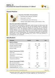
SiC <strong>UV</strong> Photodiode Selection Guide<br />
Basic Information<br />
SiC <strong>UV</strong> Photodiode Selection Guide<br />
That guide assists you selecting the right <strong>UV</strong> Silicon Carbide (SiC) based<br />
photodiode for your application. Basically this selection is between active<br />
area, spectral behaviour, packaging and additional special features. This<br />
first page is basic information and subsequent pages provide background<br />
knowledge and electronic circuit examples.<br />
About the sglux Silicon Carbide (SiC) <strong>UV</strong> photodiodes<br />
The <strong>of</strong>fered <strong>UV</strong> photodiodes base on a Silicon Carbide detector chip. SiC provides the unique<br />
property <strong>of</strong> near-perfect visible blindness, low dark <strong>current</strong>, high speed and low noise. These<br />
features make SiC the best available material for visible blind semiconductor <strong>UV</strong> detectors.<br />
The SiC detectors <strong>can</strong> be continuously operated at up to 170°C (338°F). The temperature<br />
coefficient <strong>of</strong> signal is
SiC <strong>UV</strong> Photodiode Selection Guide<br />
Background Information<br />
Table <strong>of</strong> Contents<br />
1.0 Selection <strong>of</strong> the Chip active area (photo<strong>current</strong> limits) page 2<br />
1.1 Problems with <strong>current</strong> too low (circuit linearity & temperature issues) page 3<br />
1.2 Problems with <strong>current</strong> too high (saturation) page 5<br />
1.3 Calculation <strong>of</strong> the relation between <strong>UV</strong> radiation and photo<strong>current</strong> page 5<br />
2.0 Selection <strong>of</strong> the Spectral Response page 7<br />
2.1 Unfiltered SiC page 7<br />
2.2 Filtered SiC page 8<br />
3.0 Packaging features page 9<br />
3.1 Overview page 9<br />
3.2 Drawings page 10<br />
4.0 Special features page 12<br />
Appendix A Photodiode Amplification Notes page 13<br />
Appendix B Application Note for Photodiodes page 13<br />
1.0 Selection <strong>of</strong> the Chip active area (photo<strong>current</strong> limits)<br />
The chip active area determines how many light quantum, (photons), <strong>can</strong> be collected by a<br />
photodetector. Semiconductor detectors, such as SiC <strong>UV</strong> photodiodes, convert the photons<br />
into an electrical <strong>current</strong>, the photo<strong>current</strong> I. This photo<strong>current</strong> rises linearly with the chip<br />
active area. sglux <strong>current</strong>ly <strong>of</strong>fers five different area sizes<br />
A1 = 0.06 mm 2 (S-type)<br />
A2 = 0.20 mm 2 (M-type)<br />
A3 = 0.50 mm 2 (D-type)<br />
A4 = 1.00 mm 2 (L-type)<br />
A5 = 4.00 mm 2 (XL-type)<br />
As the detector price rises with increasing active area, (see price information at p.1), the area<br />
selection basically is a compromise between costs and <strong>current</strong>.<br />
If you know the minimum and maximum irradiance you like to measure with the <strong>UV</strong><br />
photodiode the following simplified formula (1) shows a rough estimation <strong>of</strong> the photo<strong>current</strong> I<br />
given a particular chip active area AChip.<br />
Rev. 5.0 specifications subject to change without notice Page 2 [13]<br />
Manufacturer: sglux GmbH; Agent: <strong>Boston</strong> Electronics, 91 Boylston St, Brookline MA 02445 USA<br />
(800)347-5445 or (617)566-3821; fax (617)731-0935; uv@boselec.com ; www.boselec.com
SiC <strong>UV</strong> Photodiode Selection Guide<br />
I = Achip E 1.000 (1)<br />
I is the photo<strong>current</strong> in nA, Achip is the chip active area in mm 2 (enter values <strong>of</strong> 0.06 or 0.20 or<br />
1 or 4) and E is the spectral irradiance <strong>of</strong> the <strong>UV</strong> light source you like to measure in mWcm -<br />
2 nm -1 . You may find more information about photo<strong>current</strong> calculation in chapter 1.3<br />
(Calculation <strong>of</strong> the relation between <strong>UV</strong> radiation and photo<strong>current</strong>), p. 5.<br />
If you do not know the irradiance coming from your <strong>UV</strong> light source chapter 1. section 1.3<br />
gives some examples <strong>of</strong> common <strong>UV</strong> sources.<br />
The minimum <strong>current</strong> (photodiode output at lowest irradiance to be measured) should not fall<br />
below 500pA. The maximum <strong>current</strong> should not exceed 2μA and must not exceed 40μA if the<br />
component’s diode properties are to be maintained. Please refer to a detailed discussion on<br />
suitable minimum and maximum <strong>current</strong>s in the following chapters 1. section 1.1 (Problems<br />
with <strong>current</strong> too low) and 1. section 1.2 (Problems with <strong>current</strong> too high). These chapters<br />
assume a certain basic knowledge in photodiode amplifier circuits. If you are not familiar with<br />
circuits please see Appendix A (Photodiode Amplification Notes) at page 10.<br />
1.1 Problems with <strong>current</strong> too low<br />
If the <strong>current</strong> is too low, one ore more <strong>of</strong> the following problems (P1 – P4) may affect the<br />
measurement:<br />
P1 The measurement signal comes too close to the <strong>UV</strong> photodiode dark <strong>current</strong><br />
P2 High resistance feedback resistors (Rf) must be used which causes<br />
temperature drift and non linearity problems<br />
P3 Speed problems<br />
P4 Risk <strong>of</strong> electromagnetic interferences<br />
Using SiC, P1 <strong>can</strong> be neglected due to the extremely low dark <strong>current</strong> <strong>of</strong> the sglux 4H SiC <strong>UV</strong><br />
photodiodes <strong>of</strong> only some fA. P2 (temperature drift and non linearity) becomes essential<br />
from values Rf > 10 GTherefore, the photo<strong>current</strong> I should be strong enough to allow Rf<br />
values <strong>of</strong> 10 GThe relation between I and Rf is given by Ohm’s law:<br />
I = Usupply / Rf (2)<br />
where Usupply is the supply voltage <strong>of</strong> the used transimpedance amplifier. A typical value is<br />
5.00 V. Formula (2) calculates:<br />
Imin = 5.00V/10 G = 500pA (3)<br />
Rev. 5.0 specifications subject to change without notice Page 3 [13]<br />
Manufacturer: sglux GmbH; Agent: <strong>Boston</strong> Electronics, 91 Boylston St, Brookline MA 02445 USA<br />
(800)347-5445 or (617)566-3821; fax (617)731-0935; uv@boselec.com ; www.boselec.com
SiC <strong>UV</strong> Photodiode Selection Guide<br />
If a higher speed measurement is needed P3 (speed problems) could become an issue. As<br />
the SiC <strong>UV</strong> photodiode’s detection speed is extremely high (in nanoseconds only) the<br />
amplifier speed (rise time) always determines the circuit’s speed. The amplifier rise time is<br />
calculated with the following formula:<br />
= Rf Cf (4)<br />
where Cf is the feedback capacitor value which should not be lower than 0.1 nF. A lower Cf<br />
risks hitting the circuit’s resonance. Using a Cf = 0.1 nF and a Rf = 10 Gthe rise time is<br />
calculated as follows:<br />
= 10 G 0.1 nF = 1 second (5)<br />
Formula (5) shows that using a Rf = 10 Gthe circuit becomes very slow. If a higher speed is<br />
needed the photo<strong>current</strong> I must be increased to allow a decrease in the Rf value. This <strong>can</strong> be<br />
done by increasing the <strong>UV</strong> radiation or, if that is not feasible, by increasing the chip active<br />
area.<br />
The last problem (P4) that <strong>can</strong> be caused with too low photo<strong>current</strong> (= due to too small an<br />
active area) is complications from electromagnetic interferences. This is a general issue.<br />
Decreasing photo<strong>current</strong>s call for increasing shielding efforts which then increases the system<br />
price <strong>of</strong> the product. If the radiation (and thus the <strong>current</strong>) is low one should consider using a<br />
sglux TOCON pre-amplified hybrid <strong>UV</strong> sensor.<br />
Conclusion <strong>of</strong> needed minimum photo<strong>current</strong> Imin<br />
To achieve a stable temperature and linear photodiode-amplifier system the lowest<br />
measurement <strong>current</strong> Imin should be higher than 500pA. If a high speed measuring circuit is<br />
needed Imin is calculated by the following formula:<br />
Imin = Usupply Cf (6)<br />
With Usupply = 5.00V (typical value), Cf = 0.1nF (recommended value) and Rf = 10 G(lowest<br />
recommended value) the formula reduces to:<br />
Imin = 500 (7)<br />
where Imin results in nanoamperes (nA) and must be in milliseconds.<br />
In general, given these reasons, a decreasing photo<strong>current</strong> needs a more advanced amplifier<br />
design and better shielding. If you are not familiar with low <strong>current</strong> circuit development you<br />
should consider selecting a higher <strong>current</strong> (and thus larger active area) photodiode even if the<br />
price <strong>of</strong> a photodiode is higher. This strategy will provide conservative results and the initial<br />
increased financial cost will save you money in the long run.<br />
Rev. 5.0 specifications subject to change without notice Page 4 [13]<br />
Manufacturer: sglux GmbH; Agent: <strong>Boston</strong> Electronics, 91 Boylston St, Brookline MA 02445 USA<br />
(800)347-5445 or (617)566-3821; fax (617)731-0935; uv@boselec.com ; www.boselec.com
SiC <strong>UV</strong> Photodiode Selection Guide<br />
1.2 Problems with <strong>current</strong> too high (saturation)<br />
In the previous pages we discussed the calculation <strong>of</strong> a minimum recommended photodiode<br />
<strong>current</strong>. It also should be mentioned that aside from the photo<strong>current</strong> being too low too high <strong>of</strong><br />
a <strong>current</strong> may cause problems as well due to saturation effects. The saturation <strong>current</strong> Isat <strong>of</strong> a<br />
photodiode is the <strong>current</strong> limit from which the output <strong>of</strong> a photodiode turns to arbitrary values.<br />
It is determined by the photodiode’s open circuit voltage VOC and its serial resistance RS<br />
following the formula below:<br />
Isat = VOC / RS (8)<br />
A typical value (SiC photodiode) for VOC is 2.0V and for RS = 50k. The calculation is a<br />
follows:<br />
Isat = 2.0 V / (50 10 3 ) = 4 10 -5 A = 40μA.<br />
The needed minimum <strong>current</strong> (500 pA) is higher than the saturation <strong>current</strong> is higher by six<br />
orders <strong>of</strong> magnitude. Reaching the saturation limit <strong>of</strong> a SiC photodiode is therefore very<br />
unlikely.<br />
However, one should consider that a SiC <strong>UV</strong> photodiode is a sensible instrument for<br />
measurement. Even if SiC <strong>UV</strong> photodiodes are the most stable and most linear <strong>UV</strong><br />
photodiodes <strong>current</strong>ly available, values that come close to the limit should be avoided. The<br />
majority <strong>of</strong> applications use a photo<strong>current</strong> range from 1nA to 2000nA. Thus, whenever<br />
possible, the maximum <strong>current</strong> should not exceed 2000nA.<br />
1.3 Calculation <strong>of</strong> the relation between <strong>UV</strong> radiation and photo<strong>current</strong><br />
The photo<strong>current</strong> I is calculated by the following formula:<br />
I =<br />
where I is the photo<strong>current</strong> in A, Achip is the chip active area in m 2. Schip is the chip’s spectral<br />
sensitivity in AW -1 and E is the spectral irradiance <strong>of</strong> the <strong>UV</strong> light source in Wm -2 nm -1 . Due to<br />
extreme visible and IR blindness the integral value from 400nm to <strong>can</strong> be neglected even if<br />
Esource() is very strong. To get a rough estimate <strong>of</strong> the photo<strong>current</strong> generated by a certain<br />
irradiance a simplification <strong>of</strong> (9) leads to (10). That simplification assumes that the chip’s<br />
spectral sensitivity S and the <strong>UV</strong> source’s irradiance E is a constant value and does not<br />
depend on wavelength. The calculation is:<br />
I = Achip Schip E 10.000 (10)<br />
where I is the photo<strong>current</strong> in nA, Achip is the chip active area in mm 2. Schip is the chip’s<br />
spectral sensitivity in AW -1 nm -1 and E is the spectral irradiance <strong>of</strong> the <strong>UV</strong> light source in<br />
mWcm -2 nm -1 .<br />
Rev. 5.0 specifications subject to change without notice Page 5 [13]<br />
Manufacturer: sglux GmbH; Agent: <strong>Boston</strong> Electronics, 91 Boylston St, Brookline MA 02445 USA<br />
(800)347-5445 or (617)566-3821; fax (617)731-0935; uv@boselec.com ; www.boselec.com<br />
(9)
SiC <strong>UV</strong> Photodiode Selection Guide<br />
A typical value <strong>of</strong> Schip is 0.1 A/W. For further refinement please refer to the spectral response<br />
graph <strong>of</strong> the <strong>UV</strong> photodiode you are interested in (see Datasheet) or have a look at chapter<br />
2.0 (Selection <strong>of</strong> the Spectral Response, p. 7) <strong>of</strong> this guide.<br />
If you know the theoretical spectral irradiance range, (minimal and maximal values), <strong>of</strong> the <strong>UV</strong><br />
light source and you would like to measure you <strong>can</strong> easily estimate the photo<strong>current</strong> I by<br />
using formula (10) and hence select a chip active area (S-, M-, L- or XL-type) that guarantees<br />
that your minimum radiation generates a photo<strong>current</strong> <strong>of</strong> more than 500 pA and your<br />
maximum radiation generates a <strong>current</strong> <strong>of</strong>, if possible, less than 2000 nA.<br />
The following table lists some common <strong>UV</strong> applications / light sources with their spectral<br />
irradiances at peak. Please note that some simplifications apply; thus the table gives a rough<br />
estimation <strong>of</strong> photo<strong>current</strong>s for the different <strong>UV</strong> source types and different chip active areas.<br />
<strong>UV</strong> source Typ. peak E S-Type I M-Type I D-Type / L-Type I XL-Type I<br />
lacquer hardening<br />
Fe doped Hg medium<br />
pressure lamp<br />
<strong>UV</strong> sterilisation<br />
low or medium pressure<br />
Hg lamp<br />
Industrial and R&D<br />
various sources<br />
<strong>UV</strong>-Index<br />
sun<br />
Burner flame<br />
detection<br />
gas or oil flame<br />
Comments:<br />
lacquer hardening<br />
10 W/cm 2<br />
10 mW/cm 2<br />
10 μW/cm 2<br />
- 1 mW/cm 2<br />
10 μW/cm 2<br />
10 nW/cm 2<br />
600 μA<br />
600 nA with<br />
attenuated<br />
„GIGA“<br />
feature<br />
2 mA 5 mA 10 mA 40 mA<br />
600 nA 2 μA 5 μA 10 μA 40 μA<br />
0.6 - 40 nA 2 – 200 nA 5 – 500 nA 10 – 1000 nA 40 – 4000 nA<br />
600 pA 2 nA 5 nA 10 nA 40 nA<br />
600 fA 2 pA<br />
100 pA with<br />
“LENS” feature<br />
5 pA 10 pA 40 pA<br />
All <strong>current</strong> values <strong>of</strong> the standard photodiodes are too high. For lacquer hardening lamp<br />
control a special „GIGA“ attenuated photodiode will be applied. Please refer to chapter 4.0.<br />
(Special features) for more information.<br />
<strong>UV</strong> sterilisation<br />
S-chip is best. M, D, L, XL chips would work but are not needed.<br />
Industrial and R&D<br />
All chips are suited. Speed is the main consideration when selecting a chip being mindful <strong>of</strong><br />
linearity and temperature dependence values. Please contact us for further refinement.<br />
<strong>UV</strong>-Index<br />
Rev. 5.0 specifications subject to change without notice Page 6 [13]<br />
Manufacturer: sglux GmbH; Agent: <strong>Boston</strong> Electronics, 91 Boylston St, Brookline MA 02445 USA<br />
(800)347-5445 or (617)566-3821; fax (617)731-0935; uv@boselec.com ; www.boselec.com
SiC <strong>UV</strong> Photodiode Selection Guide<br />
S-Chips are too small for this application. All other chips <strong>can</strong> be applied. The reliability<br />
increases with increasing chip active area. Due to very low <strong>current</strong> the use <strong>of</strong> a TOCON (preamplified<br />
hybrid sensor) should be considered.<br />
Burner flame detection<br />
All chips are too small for this type <strong>of</strong> detection. A burner flame <strong>can</strong> be detected with the<br />
photodiode „SG10M-5Lens“. This sensor works with a concentrating lens. Please refer to<br />
chapter 4.0. (Special features), for more information. Another approach is to use a sglux<br />
TOCON_ABC1 sensor with its included pre-amplifier. The TOCON_ABC1 converts<br />
0-54 nW/cm 2 radiation into a 0-15 V output voltage.<br />
2.0 Selection <strong>of</strong> the Spectral Response<br />
This chapter assists in the selection <strong>of</strong> a spectral response pr<strong>of</strong>ile best suited for the<br />
measurement. All sglux 4H SiC <strong>UV</strong> photodiodes provide an extreme visible/IR blindness <strong>of</strong><br />
more than ten orders <strong>of</strong> magnitude. That means that the <strong>UV</strong> photodiodes reliably only<br />
measure the <strong>UV</strong> part <strong>of</strong> a radiation spectrum (and not the visible and/or infrared part), even if<br />
visible light or infrared radiation is strongly present. This is a unique feature <strong>of</strong> the<br />
semiconductor material SiC. Currently no other material provides that extreme visible<br />
blindness.<br />
2.1 Unfiltered SiC<br />
The following graph shows the spectral curve <strong>of</strong> an unfiltered 4H SiC <strong>UV</strong> photodiode.<br />
The curve’s maximum is at approximately 300nm. The response falls down to 10% <strong>of</strong><br />
maximum at 215nm, (<strong>UV</strong>C edge) and 365nm, (<strong>UV</strong>A edge). Unfiltered SiC <strong>can</strong> be used for any<br />
<strong>UV</strong> measurements where the whole <strong>UV</strong> band needs to be measured or a quasi<br />
monochromatic <strong>UV</strong> source (such as low pressure lamps) is controlled.<br />
2.2 Filtered SiC<br />
Rev. 5.0 specifications subject to change without notice Page 7 [13]<br />
Manufacturer: sglux GmbH; Agent: <strong>Boston</strong> Electronics, 91 Boylston St, Brookline MA 02445 USA<br />
(800)347-5445 or (617)566-3821; fax (617)731-0935; uv@boselec.com ; www.boselec.com
SiC <strong>UV</strong> Photodiode Selection Guide<br />
Some applications require measurement <strong>of</strong> one particular part <strong>of</strong> the <strong>UV</strong> radiation spectrum,<br />
and it is essential that other <strong>UV</strong> radiation parts do not contribute to the photodiode’s <strong>current</strong>.<br />
This requirement usually arises from standards as DVGW W294/2006 or CIE087 etc. Other<br />
applications for filtered photodiodes are <strong>UV</strong>A-<strong>UV</strong>B-<strong>UV</strong>C selective sensor probes. sglux<br />
industrially produces four different filtered SiC <strong>UV</strong> photodiode types.<br />
<strong>UV</strong>A (max = 335nm)<br />
<strong>UV</strong>B (max = 280nm)<br />
<strong>UV</strong>C (max = 270nm)<br />
<strong>UV</strong>-Index (following CIE087 curve)<br />
The following graph shows the four different spectra.<br />
The graph assigns the filtered photodiode’s spectral response to an individual wavelength.<br />
The following table extracts the most important specifications.<br />
Filter type Wavelength Sensitivity Wavelength Wavelength Visible<br />
<strong>of</strong> max.<br />
at max.<br />
10% left side 10% right side Blindness<br />
no filter (BBand) 300 nm 0.10 A/W 215 nm 365 nm >10 10<br />
<strong>UV</strong>A 335 nm 0.06 A/W 310 nm 370 nm >10 10<br />
<strong>UV</strong>B 280 nm 0.09 A/W 230 nm 315 nm >10 10<br />
<strong>UV</strong>C 270 nm 0.10 A/W 230 nm 285 nm >10 10<br />
ERYTHEMA 300 nm 0.90 A/W _ 310 nm >10 10<br />
Other spectral specifications are available on request.<br />
Rev. 5.0 specifications subject to change without notice Page 8 [13]<br />
Manufacturer: sglux GmbH; Agent: <strong>Boston</strong> Electronics, 91 Boylston St, Brookline MA 02445 USA<br />
(800)347-5445 or (617)566-3821; fax (617)731-0935; uv@boselec.com ; www.boselec.com
SiC <strong>UV</strong> Photodiode Selection Guide<br />
g<br />
3.0 Packaging features<br />
All sglux SiC <strong>UV</strong> photodiodes use a hermetically sealed melted window metal package. Each<br />
photodiode is gross and fine leak tested before sales. Two different sizes, (TO18 and TO5),<br />
with corresponding different heights and pin terminals are <strong>of</strong>fered.<br />
The reason for the different packaging types are technical in nature, (field <strong>of</strong> view, electrically<br />
floating housing, etc.) or just to allow the replacement <strong>of</strong> a previously applied photodiode by<br />
keeping the geometric parameters.<br />
3.1 Overview<br />
The below table illustrates the different packaging selection opportunities.<br />
sample<br />
picture<br />
selection description<br />
code<br />
18 TO18 Ni plated housing, 5.6 mm diameter, 5.2 mm height two gold plated pins<br />
(Anode grounded and Cathode isolated).<br />
18ISO90 TO18 Ni plated housing, 5.6 mm diameter, 5.2 mm height three gold plated pins<br />
(Anode and Cathode isolated, additional third pin for optional grounding <strong>of</strong> the body).<br />
18S TO18 Ni plated short housing, 5.6 mm diameter, 3.8 mm height two gold plated pins<br />
(Anode grounded and Cathode isolated). Not available with filters.<br />
5 TO5 Ni plated housing, 9.2 mm diameter, 4.3 mm height (unfiltered photodiodes), 6.6<br />
mm height (filtered photodiodes), two gold plated pins (Anode grounded and<br />
Cathode isolated).<br />
5ISO90 TO5 Ni plated housing, 9.2 mm diameter, 4.3 mm height (unfiltered photodiodes), 6.6<br />
mm height (filtered photodiodes), three gold plated pins (Anode and Cathode<br />
isolated, additional third pin for optional grounding <strong>of</strong> the body).<br />
Rev. 5.0 specifications subject to change without notice Page 9 [13]<br />
Manufacturer: sglux GmbH; Agent: <strong>Boston</strong> Electronics, 91 Boylston St, Brookline MA 02445 USA<br />
(800)347-5445 or (617)566-3821; fax (617)731-0935; uv@boselec.com ; www.boselec.com
SiC <strong>UV</strong> Photodiode Selection Guide<br />
3.2 Drawings<br />
Selection code “18” TO18 Ni plated housing, 5.6 mm diameter, 5.2 mm height two gold<br />
plated pins (Anode grounded and Cathode isolated).<br />
Selection code “18ISO90” TO18 Ni plated housing, 5.6 mm diameter, 5.2 mm height three<br />
gold plated pins (Anode and Cathode isolated, additional third pin for optional grounding <strong>of</strong> the<br />
body).<br />
Selection code “18S” TO18 Ni plated short housing, 5.6 mm diameter, 3.8 mm height two<br />
gold plated pins (Anode grounded and Cathode isolated). Not available with filters.<br />
Rev. 5.0 specifications subject to change without notice Page 10 [13]<br />
Manufacturer: sglux GmbH; Agent: <strong>Boston</strong> Electronics, 91 Boylston St, Brookline MA 02445 USA<br />
(800)347-5445 or (617)566-3821; fax (617)731-0935; uv@boselec.com ; www.boselec.com
SiC <strong>UV</strong> Photodiode Selection Guide<br />
Selection Code ”5” (photodiodes without filters) TO5 Ni plated housing, 9.2 mm diameter,<br />
4.3 mm height, two gold plated pins (Anode grounded and Cathode isolated).<br />
Selection Code ”5” (photodiodes with filters) TO5 Ni plated housing, 9.2 mm diameter, 6.6<br />
mm height, two gold plated pins (Anode grounded and Cathode isolated).<br />
Rev. 5.0 specifications subject to change without notice Page 11 [13]<br />
Manufacturer: sglux GmbH; Agent: <strong>Boston</strong> Electronics, 91 Boylston St, Brookline MA 02445 USA<br />
(800)347-5445 or (617)566-3821; fax (617)731-0935; uv@boselec.com ; www.boselec.com
SiC <strong>UV</strong> Photodiode Selection Guide<br />
4.0 Special features<br />
Besides the three main selection criteria chip active area, spectral response and packaging<br />
details some special features <strong>can</strong> be added to the photodiode’s properties. These special<br />
features are useful if the <strong>UV</strong> radiation is extremely high or low or if the working temperature is<br />
high. The below table shows the selectable special features.<br />
selection code description<br />
Lens Concentrating Lens creating a virtual active area <strong>of</strong> 55 real active area. This<br />
approximately multiplies the <strong>current</strong> by factor 55 while using the same chip active<br />
area. A disadvantage is a strongly reduced field <strong>of</strong> view compared with the flat<br />
window type.<br />
MEGA special attenuated photodiode for very strong <strong>UV</strong> radiation up to 500 mW/cm 2<br />
GIGA special attenuated photodiode for extreme <strong>UV</strong> radiation up to 7000 mW/cm 2<br />
Appendix A Photodiode Amplification Notes<br />
For a correct reading <strong>of</strong> the photodiode the <strong>current</strong> (and not the voltage) must be analyzed.<br />
This requires a short circuiting <strong>of</strong> the photodiode. Usual approaches are using a<br />
Picoamperemeter such as Keithley 617 or a transimpedance amplifier circuit as shown below.<br />
The adjacent design gives an example <strong>of</strong> a<br />
simple amplifier circuit. At the left side the<br />
photodiode is shown. The upper connection<br />
is the Cathode (isolated pin <strong>of</strong> the<br />
photodiode) and the lower connection is the<br />
Anode (usually grounded pin <strong>of</strong> the<br />
photodiode).<br />
We recommend using a Texas Instruments<br />
OPA336 transimpedance amplifier.<br />
The OPA336 is a low priced amplifier that is sufficient for the majority <strong>of</strong> applications.<br />
Appendix B Application Note for Photodiodes<br />
Rev. 5.0 specifications subject to change without notice Page 12 [13]<br />
Manufacturer: sglux GmbH; Agent: <strong>Boston</strong> Electronics, 91 Boylston St, Brookline MA 02445 USA<br />
(800)347-5445 or (617)566-3821; fax (617)731-0935; uv@boselec.com ; www.boselec.com
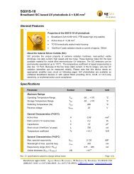
SG01S-18<br />
Broadband SiC based <strong>UV</strong> photodiode A = 0,06 mm 2<br />
General Features<br />
Properties <strong>of</strong> the SG01S-18 <strong>UV</strong> photodiode<br />
Broadband <strong>UV</strong>A+<strong>UV</strong>B+<strong>UV</strong>C, PTB tested high chip stability<br />
Active Area A = 0,06 mm 2<br />
About the material Silicon Carbide (SiC)<br />
TO18 hermetically sealed metal housing<br />
10mW/cm 2 peak radiation results a <strong>current</strong> <strong>of</strong> approx. 780nA<br />
SiC provides the unique property <strong>of</strong> extreme radiation hardness, near-perfect visible<br />
blindness, low dark <strong>current</strong>, high speed and low noise. These features make SiC the best<br />
available material for visible blind semiconductor <strong>UV</strong> detectors. The SiC detectors <strong>can</strong> be<br />
permanently operated at up to 170°C. The temperature coefficient <strong>of</strong> signal (responsivity) is<br />
also low, 10 10 -<br />
Rev. 5.1 specifications subject to change without notice Page 1 [3]<br />
Manufacturer: sglux GmbH; Agent: <strong>Boston</strong> Electronics, 91 Boylston St, Brookline NA 02445 USA<br />
(800)347-5445 or (617)566-3821; fax (617)731-0935; uv@boselec.com ; www.boselec.com
SG01S-18<br />
Broadband SiC based <strong>UV</strong> photodiode A = 0,06 mm 2<br />
Spectral Response<br />
Circuit Viewing Angle<br />
Drawing<br />
Rev. 5.1 specifications subject to change without notice Page 2 [3]<br />
Manufacturer: sglux GmbH; Agent: <strong>Boston</strong> Electronics, 91 Boylston St, Brookline NA 02445 USA<br />
(800)347-5445 or (617)566-3821; fax (617)731-0935; uv@boselec.com ; www.boselec.com
SG01S-18ISO90<br />
Broadband SiC based <strong>UV</strong> photodiode A = 0,06 mm 2<br />
General Features<br />
Properties <strong>of</strong> the SG01S-18ISO90 <strong>UV</strong> photodiode<br />
Broadband <strong>UV</strong>A+<strong>UV</strong>B+<strong>UV</strong>C photodiode<br />
Active Area A = 0,06 mm 2<br />
About the material Silicon Carbide (SiC)<br />
TO18 herm. sealed housing, both pins isolated & in a circle<br />
10mW/cm 2 peak radiation results a <strong>current</strong> <strong>of</strong> approx. 400nA<br />
SiC provides the unique property <strong>of</strong> extreme radiation hardness, near-perfect visible<br />
blindness, low dark <strong>current</strong>, high speed and low noise. These features make SiC the best<br />
available material for visible blind semiconductor <strong>UV</strong> detectors. The SiC detectors <strong>can</strong> be<br />
permanently operated at up to 170°C. The temperature coefficient <strong>of</strong> signal (responsivity) is<br />
also low, 10 10 -<br />
Rev. 5.0 specifications subject to change without notice Page 1 [3]<br />
Manufacturer: sglux GmbH; Agent: <strong>Boston</strong> Electronics, 91 Boylston St, Brookline NA 02445 USA<br />
(800)347-5445 or (617)566-3821; fax (617)731-0935; uv@boselec.com ; www.boselec.com
SG01S-18ISO90<br />
Broadband SiC based <strong>UV</strong> photodiode A = 0,06 mm 2<br />
Spectral Response<br />
Circuit Viewing Angle<br />
Drawing<br />
Rev. 5.0 specifications subject to change without notice Page 2 [3]<br />
Manufacturer: sglux GmbH; Agent: <strong>Boston</strong> Electronics, 91 Boylston St, Brookline NA 02445 USA<br />
(800)347-5445 or (617)566-3821; fax (617)731-0935; uv@boselec.com ; www.boselec.com
SG01S-A18<br />
<strong>UV</strong>A-only SiC based <strong>UV</strong> photodiode A = 0,06 mm 2<br />
General Features<br />
Properties <strong>of</strong> the SG01S-A18 <strong>UV</strong> photodiode<br />
<strong>UV</strong>A-only sensitivity, PTB tested high chip stability<br />
Active Area A = 0,06 mm 2<br />
TO18 hermetically sealed housing<br />
About the material Silicon Carbide (SiC)<br />
10mW/cm 2 radiation at 335nm results a <strong>current</strong> <strong>of</strong> approx. 360nA<br />
SiC provides the unique property <strong>of</strong> extreme radiation hardness, near-perfect visible<br />
blindness, low dark <strong>current</strong>, high speed and low noise. These features make SiC the best<br />
available material for visible blind semiconductor <strong>UV</strong> detectors. The SiC detectors <strong>can</strong> be<br />
permanently operated at up to 170°C. The temperature coefficient <strong>of</strong> signal (responsivity) is<br />
also low, 10 10 -<br />
Rev. 5.1 specifications subject to change without notice Page 1 [3]<br />
Manufacturer: sglux GmbH; Agent: <strong>Boston</strong> Electronics, 91 Boylston St, Brookline NA 02445 USA<br />
(800)347-5445 or (617)566-3821; fax (617)731-0935; uv@boselec.com ; www.boselec.com
SG01S-A18<br />
<strong>UV</strong>A-only SiC based <strong>UV</strong> photodiode A = 0,06 mm 2<br />
Spectral Response<br />
Circuit Viewing Angle<br />
Drawing<br />
Rev. 5.1 specifications subject to change without notice Page 2 [3]<br />
Manufacturer: sglux GmbH; Agent: <strong>Boston</strong> Electronics, 91 Boylston St, Brookline NA 02445 USA<br />
(800)347-5445 or (617)566-3821; fax (617)731-0935; uv@boselec.com ; www.boselec.com
SG01S-B18<br />
<strong>UV</strong>B-only SiC based <strong>UV</strong> photodiode A = 0,06 mm 2<br />
General Features<br />
Properties <strong>of</strong> the SG01S-B18 <strong>UV</strong> photodiode<br />
<strong>UV</strong>B-only sensitivity, compliant with CIE078<br />
Active Area A = 0,06 mm 2<br />
About the material Silicon Carbide (SiC)<br />
TO18 hermetically sealed housing, PTB tested high chip stability<br />
10mW/cm 2 radiation at peak results a <strong>current</strong> <strong>of</strong> approx. 350nA<br />
SiC provides the unique property <strong>of</strong> extreme radiation hardness, near-perfect visible<br />
blindness, low dark <strong>current</strong>, high speed and low noise. These features make SiC the best<br />
available material for visible blind semiconductor <strong>UV</strong> detectors. The SiC detectors <strong>can</strong> be<br />
permanently operated at up to 170°C. The temperature coefficient <strong>of</strong> signal (responsivity) is<br />
also low, 10 10 -<br />
Rev. 5.1 specifications subject to change without notice Page 1 [3]<br />
Manufacturer: sglux GmbH; Agent: <strong>Boston</strong> Electronics, 91 Boylston St, Brookline NA 02445 USA<br />
(800)347-5445 or (617)566-3821; fax (617)731-0935; uv@boselec.com ; www.boselec.com
SG01S-B18<br />
<strong>UV</strong>B-only SiC based <strong>UV</strong> photodiode A = 0,06 mm 2<br />
Spectral Response<br />
Circuit Viewing Angle<br />
Drawing<br />
Rev. 5.1 specifications subject to change without notice Page 2 [3]<br />
Manufacturer: sglux GmbH; Agent: <strong>Boston</strong> Electronics, 91 Boylston St, Brookline NA 02445 USA<br />
(800)347-5445 or (617)566-3821; fax (617)731-0935; uv@boselec.com ; www.boselec.com
SG01S-C18<br />
<strong>UV</strong>C-only SiC based <strong>UV</strong> photodiode A = 0,06 mm 2<br />
General Features<br />
Properties <strong>of</strong> the SG01S-C18 <strong>UV</strong> photodiode<br />
<strong>UV</strong>C-only sensitivity compliant with DVGW W294<br />
Active Area A = 0,06 mm 2<br />
About the material Silicon Carbide (SiC)<br />
TO18 hermetically sealed housing, PTB tested high chip stability<br />
10mW/cm 2 radiation at 254nm results a <strong>current</strong> <strong>of</strong> approx. 315nA<br />
SiC provides the unique property <strong>of</strong> extreme radiation hardness, near-perfect visible<br />
blindness, low dark <strong>current</strong>, high speed and low noise. These features make SiC the best<br />
available material for visible blind semiconductor <strong>UV</strong> detectors. The SiC detectors <strong>can</strong> be<br />
permanently operated at up to 170°C. The temperature coefficient <strong>of</strong> signal (responsivity) is<br />
also low, 10 10 -<br />
Rev. 5.1 specifications subject to change without notice Page 1 [3]<br />
Manufacturer: sglux GmbH; Agent: <strong>Boston</strong> Electronics, 91 Boylston St, Brookline NA 02445 USA<br />
(800)347-5445 or (617)566-3821; fax (617)731-0935; uv@boselec.com ; www.boselec.com
SG01S-C18<br />
<strong>UV</strong>C-only SiC based <strong>UV</strong> photodiode A = 0,06 mm 2<br />
Spectral Response<br />
Circuit Viewing Angle<br />
Drawing<br />
Rev. 5.1 specifications subject to change without notice Page 2 [3]<br />
Manufacturer: sglux GmbH; Agent: <strong>Boston</strong> Electronics, 91 Boylston St, Brookline NA 02445 USA<br />
(800)347-5445 or (617)566-3821; fax (617)731-0935; uv@boselec.com ; www.boselec.com
SG01S-C5<br />
<strong>UV</strong>C-only SiC based <strong>UV</strong> photodiode A = 0,06 mm 2<br />
General Features<br />
Properties <strong>of</strong> the SG01S-C5 <strong>UV</strong> photodiode<br />
<strong>UV</strong>C-only sensitivity according to DVGW W294<br />
Active Area A = 0,06 mm 2<br />
TO5 hermetically sealed housing<br />
About the material Silicon Carbide (SiC)<br />
10mW/cm 2 radiation at 254nm results a <strong>current</strong> <strong>of</strong> approx. 210nA<br />
SiC provides the unique property <strong>of</strong> extreme radiation hardness, near-perfect visible<br />
blindness, low dark <strong>current</strong>, high speed and low noise. These features make SiC the best<br />
available material for visible blind semiconductor <strong>UV</strong> detectors. The SiC detectors <strong>can</strong> be<br />
permanently operated at up to 170°C. The temperature coefficient <strong>of</strong> signal (responsivity) is<br />
also low, 10 10 -<br />
Rev. 5.0 specifications subject to change without notice Page 1 [3]<br />
Manufacturer: sglux GmbH; Agent: <strong>Boston</strong> Electronics, 91 Boylston St, Brookline NA 02445 USA<br />
(800)347-5445 or (617)566-3821; fax (617)731-0935; uv@boselec.com ; www.boselec.com
SG01S-C5<br />
<strong>UV</strong>C-only SiC based <strong>UV</strong> photodiode A = 0,06 mm 2<br />
Spectral Response<br />
Circuit Viewing Angle<br />
Drawing<br />
Rev. 5.0 specifications subject to change without notice Page 2 [3]<br />
Manufacturer: sglux GmbH; Agent: <strong>Boston</strong> Electronics, 91 Boylston St, Brookline NA 02445 USA<br />
(800)347-5445 or (617)566-3821; fax (617)731-0935; uv@boselec.com ; www.boselec.com
SG01S-18S<br />
Broadband SiC based <strong>UV</strong> photodiode A = 0,06 mm 2<br />
General Features<br />
Properties <strong>of</strong> the SG01S-18S <strong>UV</strong> photodiode<br />
Broadband <strong>UV</strong>A+<strong>UV</strong>B+<strong>UV</strong>C photodiode<br />
Active Area A = 0,06 mm 2<br />
About the material Silicon Carbide (SiC)<br />
TO18 hermetically sealed metal housing, short cap<br />
10mW/cm 2 peak radiation results a <strong>current</strong> <strong>of</strong> approx. 400nA<br />
SiC provides the unique property <strong>of</strong> extreme radiation hardness, near-perfect visible<br />
blindness, low dark <strong>current</strong>, high speed and low noise. These features make SiC the best<br />
available material for visible blind semiconductor <strong>UV</strong> detectors. The SiC detectors <strong>can</strong> be<br />
permanently operated at up to 170°C. The temperature coefficient <strong>of</strong> signal (responsivity) is<br />
also low, 10 10 -<br />
Rev. 5.0 specifications subject to change without notice Page 1 [4]<br />
Manufacturer: sglux GmbH; Agent: <strong>Boston</strong> Electronics, 91 Boylston St, Brookline NA 02445 USA<br />
(800)347-5445 or (617)566-3821; fax (617)731-0935; uv@boselec.com ; www.boselec.com
SG01S-18S<br />
Broadband SiC based <strong>UV</strong> photodiode A = 0,06 mm 2<br />
Spectral Response<br />
Circuit Viewing Angle<br />
Drawing<br />
Rev. 5.0 specifications subject to change without notice Page 2 [4]<br />
Manufacturer: sglux GmbH; Agent: <strong>Boston</strong> Electronics, 91 Boylston St, Brookline NA 02445 USA<br />
(800)347-5445 or (617)566-3821; fax (617)731-0935; uv@boselec.com ; www.boselec.com
SG01D-18<br />
Broadband SiC based <strong>UV</strong> photodiode A = 0,50 mm 2<br />
General Features<br />
Properties <strong>of</strong> the SG01M-18 <strong>UV</strong> photodiode<br />
Broadband <strong>UV</strong>A+<strong>UV</strong>B+<strong>UV</strong>C, PTB tested high chip stability<br />
Active Area A = 0,50 mm 2<br />
About the material Silicon Carbide (SiC)<br />
TO18 hermetically sealed metal housing<br />
10μ/cm 2 peak radiation results a <strong>current</strong> <strong>of</strong> approx. 6,5 nA<br />
SiC provides the unique property <strong>of</strong> extreme radiation hardness, near-perfect visible<br />
blindness, low dark <strong>current</strong>, high speed and low noise. These features make SiC the best<br />
available material for visible blind semiconductor <strong>UV</strong> detectors. The SiC detectors <strong>can</strong> be<br />
permanently operated at up to 170°C. The temperature coefficient <strong>of</strong> signal (responsivity) is<br />
also low, 10 10 -<br />
Rev. 5.1 specifications subject to change without notice Page 1 [4]<br />
Manufacturer: sglux GmbH; Agent: <strong>Boston</strong> Electronics, 91 Boylston St, Brookline MA 02445 USA<br />
(800)347-5445 or (617)566-3821; fax (617)731-0935; uv@boselec.com ; www.boselec.com
SG01D-18<br />
Broadband SiC based <strong>UV</strong> photodiode A = 0,50 mm 2<br />
Spectral Response<br />
Circuit Viewing Angle<br />
Drawing<br />
Rev. 5.1 specifications subject to change without notice Page 2 [4]<br />
Manufacturer: sglux GmbH; Agent: <strong>Boston</strong> Electronics, 91 Boylston St, Brookline MA 02445 USA<br />
(800)347-5445 or (617)566-3821; fax (617)731-0935; uv@boselec.com ; www.boselec.com
SG01M-18<br />
Broadband SiC based <strong>UV</strong> photodiode A = 0,20 mm 2<br />
General Features<br />
Properties <strong>of</strong> the SG01M-18 <strong>UV</strong> photodiode<br />
Broadband <strong>UV</strong>A+<strong>UV</strong>B+<strong>UV</strong>C photodiode<br />
Active Area A = 0,20 mm 2<br />
About the material Silicon Carbide (SiC)<br />
TO18 hermetically sealed metal housing<br />
10mW/cm 2 peak radiation results a <strong>current</strong> <strong>of</strong> approx. 2600nA<br />
SiC provides the unique property <strong>of</strong> extreme radiation hardness, near-perfect visible<br />
blindness, low dark <strong>current</strong>, high speed and low noise. These features make SiC the best<br />
available material for visible blind semiconductor <strong>UV</strong> detectors. The SiC detectors <strong>can</strong> be<br />
permanently operated at up to 170°C. The temperature coefficient <strong>of</strong> signal (responsivity) is<br />
also low, 10 10 -<br />
Rev. 5.0 specifications subject to change without notice Page 1 [3]<br />
Manufacturer: sglux GmbH; Agent: <strong>Boston</strong> Electronics, 91 Boylston St, Brookline NA 02445 USA<br />
(800)347-5445 or (617)566-3821; fax (617)731-0935; uv@boselec.com ; www.boselec.com
SG01M-18<br />
Broadband SiC based <strong>UV</strong> photodiode A = 0,20 mm 2<br />
Spectral Response<br />
Circuit Viewing Angle<br />
Drawing<br />
Rev. 5.0 specifications subject to change without notice Page 2 [3]<br />
Manufacturer: sglux GmbH; Agent: <strong>Boston</strong> Electronics, 91 Boylston St, Brookline NA 02445 USA<br />
(800)347-5445 or (617)566-3821; fax (617)731-0935; uv@boselec.com ; www.boselec.com
SG01M-E18 (ERYCA_custom)<br />
high precision <strong>UV</strong>-Index photodiode<br />
General Features<br />
Properties <strong>of</strong> the ERYCA_custom photodiode<br />
DIN5050/ CIE087 <strong>UV</strong>-Index measurement with very small error < 3%<br />
TO18 hermetically sealed housing, 1 <strong>UV</strong>I (2,5 μW/cm2) 500 pA<br />
Information about the <strong>UV</strong>-Index (<strong>UV</strong>I)<br />
The <strong>UV</strong> index is an international standard measurement <strong>of</strong> how strong the ultraviolet (<strong>UV</strong>)<br />
radiation from the sun is at a particular place on a particular day. It is a scale primarily used in<br />
daily forecasts aimed at the general public. The <strong>UV</strong>-Index is calculated by integrating the<br />
sun’s <strong>UV</strong> spectrum multiplied with the Erythema action curve (fig. 1, black curve and fig. 2,<br />
formula 1). That integral is divided by 25 mW/m 2 to generate a convenient index value, which<br />
becomes essentially a scale <strong>of</strong> 0 to 10. The Erythema action curve is a wavelength resolved<br />
measure <strong>of</strong> the sunburn danger. It is maximised at 297nm (<strong>UV</strong>B) and then strongly decreases<br />
towards <strong>UV</strong>A radiation. Literature: A. F. McKinlay and B. L. Diffey, “A reference action<br />
spectrum for ultraviolet induced erythema in human skin” CIE Journal, 6-1, 17-22 (1987)<br />
About the sglux ERYCA sensors<br />
The ERYCA is designed for accurate measurement <strong>of</strong> the <strong>UV</strong>-Index. ERYCA’s error is
SG01M-E18 (ERYCA_custom)<br />
high precision <strong>UV</strong>-Index photodiode<br />
Fig. 1 Spectral Response<br />
Fig. 2 Calculation Formulae Fig. 3 Error Graph<br />
Fig. 4 Sun Spectra Issued by the Swiss Meteo Institute<br />
Rev. 5.0 specifications subject to change without notice Page 2 [4]<br />
Manufacturer: sglux GmbH; Agent: <strong>Boston</strong> Electronics, 91 Boylston St, Brookline NA 02445 USA<br />
(800)347-5445 or (617)566-3821; fax (617)731-0935; uv@boselec.com ; www.boselec.com
SG01M-E18 (ERYCA_custom)<br />
high precision <strong>UV</strong>-Index photodiode<br />
Specifications<br />
Parameter Symbol Value Unit<br />
Maximum Ratings<br />
Operating Temperature Range Topt -55 … +170 °C<br />
Storage Temperature Range Tstor -55 … +170 °C<br />
Soldering Temperature (3s) Tsold 260 °C<br />
Reverse voltage VRmax 20 V<br />
General Characteristics (T=25°C)<br />
Active Area A 0,20 mm 2<br />
Dark <strong>current</strong> (1V reverse bias) Id 1 fA<br />
Capacitance C 75 pF<br />
Short circuit (1 <strong>UV</strong>I) I0 500 pA<br />
Temperature coefficient Tc
SG01L-18<br />
Broadband SiC based <strong>UV</strong> photodiode A = 1,0 mm 2<br />
General Features<br />
Properties <strong>of</strong> the SG01L-18 <strong>UV</strong> photodiode<br />
Broadband <strong>UV</strong>A+<strong>UV</strong>B+<strong>UV</strong>C photodiode<br />
Active Area A = 1,0 mm 2<br />
About the material Silicon Carbide (SiC)<br />
TO18 hermetically sealed metal housing<br />
10μW/cm 2 peak radiation results a <strong>current</strong> <strong>of</strong> approx. 12nA<br />
SiC provides the unique property <strong>of</strong> extreme radiation hardness, near-perfect visible<br />
blindness, low dark <strong>current</strong>, high speed and low noise. These features make SiC the best<br />
available material for visible blind semiconductor <strong>UV</strong> detectors. The SiC detectors <strong>can</strong> be<br />
permanently operated at up to 170°C. The temperature coefficient <strong>of</strong> signal (responsivity) is<br />
also low, 10 10 -<br />
Rev. 5.1 specifications subject to change without notice Page 1 [2]<br />
Manufacturer: sglux GmbH; Agent: <strong>Boston</strong> Electronics, 91 Boylston St, Brookline MA 02445 USA<br />
(800)347-5445 or (617)566-3821; fax (617)731-0935; uv@boselec.com ; www.boselec.com
SG01L-18<br />
Broadband SiC based <strong>UV</strong> photodiode A = 1,0 mm 2<br />
Spectral Response<br />
Circuit Viewing Angle<br />
Drawing<br />
Rev. 5.1 specifications subject to change without notice Page 2 [2]<br />
Manufacturer: sglux GmbH; Agent: <strong>Boston</strong> Electronics, 91 Boylston St, Brookline MA 02445 USA<br />
(800)347-5445 or (617)566-3821; fax (617)731-0935; uv@boselec.com ; www.boselec.com
SG01XL-5<br />
Broadband SiC based <strong>UV</strong> photodiode A = 4,00 mm 2<br />
General Features<br />
Properties <strong>of</strong> the SG01XL-5 <strong>UV</strong> photodiode<br />
Broadband <strong>UV</strong>A+<strong>UV</strong>B+<strong>UV</strong>C photodiode<br />
Active Area A = 4,00 mm 2<br />
About the material Silicon Carbide (SiC)<br />
TO5 hermetically sealed metal housing<br />
1μW/cm 2 peak radiation results a <strong>current</strong> <strong>of</strong> approx. 5nA<br />
SiC provides the unique property <strong>of</strong> extreme radiation hardness, near-perfect visible<br />
blindness, low dark <strong>current</strong>, high speed and low noise. These features make SiC the best<br />
available material for visible blind semiconductor <strong>UV</strong> detectors. The SiC detectors <strong>can</strong> be<br />
permanently operated at up to 170°C. The temperature coefficient <strong>of</strong> signal (responsivity) is<br />
also low, 10 10 -<br />
Rev. 5.0 specifications subject to change without notice Page 1 [3]<br />
Manufacturer: sglux GmbH; Agent: <strong>Boston</strong> Electronics, 91 Boylston St, Brookline MA 02445 USA<br />
(800)347-5445 or (617)566-3821; fax (617)731-0935; uv@boselec.com ; www.boselec.com
SG01XL-5<br />
Broadband SiC based <strong>UV</strong> photodiode A = 4,00 mm 2<br />
Spectral Response<br />
Circuit<br />
Drawing<br />
Viewing Angle<br />
Rev. 5.0 specifications subject to change without notice Page 2 [3]<br />
Manufacturer: sglux GmbH; Agent: <strong>Boston</strong> Electronics, 91 Boylston St, Brookline MA 02445 USA<br />
(800)347-5445 or (617)566-3821; fax (617)731-0935; uv@boselec.com ; www.boselec.com
AG28S<br />
<strong>UV</strong>C sensitive AlGaN based <strong>UV</strong> photodiode A = 0,076 mm 2<br />
General Features<br />
Properties <strong>of</strong> the AG28S <strong>UV</strong> photodiode<br />
<strong>UV</strong>C sensitive photodiode<br />
Active Area A = 0,076 mm 2<br />
TO18 metal housing<br />
10mW/cm 2 peak radiation results a <strong>current</strong> <strong>of</strong> approx. 240 nA<br />
About the material (Aluminium)Gallium Nitride (Al)GaN<br />
(Al)GaN is a new semiconductor material for visible blind <strong>UV</strong> photodiodes. By modification<br />
<strong>of</strong> the Al – to - Ga stoichiometry it is possible to produce photodiodes with different spectral<br />
behaviour. This allows to <strong>of</strong>fer Photodiodes sensible for broad band <strong>UV</strong> (<strong>UV</strong>A+<strong>UV</strong>B+<strong>UV</strong>C),<br />
for <strong>UV</strong>B-only and for <strong>UV</strong>C only without using a filter.<br />
Specifications<br />
Parameter Symbol Value Unit<br />
Maximum Ratings<br />
Operating Temperature Range Topt -25 … +70 °C<br />
Storage Temperature Range Tstor 0 … +100 °C<br />
Soldering Temperature (3s) Tsold 260 °C<br />
Reverse voltage VRmax 5 V<br />
General Characteristics (T=25°C)<br />
Active Area A 0,076 mm 2<br />
Dark <strong>current</strong> (1V reverse bias) Id 100 fA<br />
Capacitance C 24 pF<br />
Short circuit (10mW/cm 2 at peak) I0 240 nA<br />
Temperature coefficient Tc 400nm) VB 10 3 -<br />
Rev. 3.1 Page 1 [2]<br />
Manufacturer: sglux GmbH; Agent: <strong>Boston</strong> Electronics, 91 Boylston St, Brookline MA 02445 USA<br />
(800)347-5445 or (617)566-3821; fax (617)731-0935; uv@boselec.com; www.boselec.com
AG28S<br />
<strong>UV</strong>C sensitive AlGaN based <strong>UV</strong> photodiode A = 0,076 mm 2<br />
Spectral Response<br />
Circuit Viewing Angle<br />
Drawing<br />
Rev. 3.1 Page 2 [2]<br />
Manufacturer: sglux GmbH; Agent: <strong>Boston</strong> Electronics, 91 Boylston St, Brookline MA 02445 USA<br />
(800)347-5445 or (617)566-3821; fax (617)731-0935; uv@boselec.com; www.boselec.com
AG32S<br />
<strong>UV</strong>B sensitive AlGaN based <strong>UV</strong> photodiode A = 0,076 mm 2<br />
General Features<br />
Properties <strong>of</strong> the AG32S <strong>UV</strong> photodiode<br />
<strong>UV</strong>B sensitive photodiode<br />
Active Area A = 0,076 mm 2<br />
TO18 metal housing<br />
10mW/cm 2 peak radiation results a <strong>current</strong> <strong>of</strong> approx. 700 nA<br />
About the material (Aluminium)Gallium Nitride (Al)GaN<br />
(Al)GaN is a new semiconductor material for visible blind <strong>UV</strong> photodiodes. By modification<br />
<strong>of</strong> the Al – to - Ga stoichiometry it is possible to produce photodiodes with different spectral<br />
behaviour. This allows to <strong>of</strong>fer Photodiodes sensible for broad band <strong>UV</strong> (<strong>UV</strong>A+<strong>UV</strong>B+<strong>UV</strong>C),<br />
for <strong>UV</strong>B-only and for <strong>UV</strong>C only without using a filter.<br />
Specifications<br />
Parameter Symbol Value Unit<br />
Maximum Ratings<br />
Operating Temperature Range Topt -25 … +70 °C<br />
Storage Temperature Range Tstor 0 … +100 °C<br />
Soldering Temperature (3s) Tsold 260 °C<br />
Reverse voltage VRmax 5 V<br />
General Characteristics (T=25°C)<br />
Active Area A 0,076 mm 2<br />
Dark <strong>current</strong> (1V reverse bias) Id 100 fA<br />
Capacitance C 24 pF<br />
Short circuit (10mW/cm 2 at peak) I0 700 nA<br />
Temperature coefficient Tc 400nm) VB 10 3 -<br />
Rev. 3.1 Page 1 [2]<br />
Manufacturer: sglux GmbH; Agent: <strong>Boston</strong> Electronics, 91 Boylston St, Brookline MA 02445 USA<br />
(800)347-5445 or (617)566-3821; fax (617)731-0935; uv@boselec.com ; www.boselec.com
AG32S<br />
<strong>UV</strong>B sensitive AlGaN based <strong>UV</strong> photodiode A = 0,076 mm 2<br />
Spectral Response<br />
Circuit Viewing Angle<br />
Drawing<br />
Rev. 3.1 Page 2 [2]<br />
Manufacturer: sglux GmbH; Agent: <strong>Boston</strong> Electronics, 91 Boylston St, Brookline MA 02445 USA<br />
(800)347-5445 or (617)566-3821; fax (617)731-0935; uv@boselec.com ; www.boselec.com
AG38S<br />
Broad Band (Al)GaN based <strong>UV</strong> photodiode A = 0,076 mm 2<br />
General Features<br />
Properties <strong>of</strong> the AG38S <strong>UV</strong> photodiode<br />
Broad Band <strong>UV</strong>A+<strong>UV</strong>B+<strong>UV</strong>C photodiode<br />
Active Area A = 0,076 mm 2<br />
TO18 metal housing<br />
10mW/cm 2 peak radiation results a <strong>current</strong> <strong>of</strong> approx. 700 nA<br />
About the material (Aluminium)Gallium Nitride (Al)GaN<br />
(Al)GaN is a new semiconductor material for visible blind <strong>UV</strong> photodiodes. By modification<br />
<strong>of</strong> the Al – to - Ga stoichiometry it is possible to produce photodiodes with different spectral<br />
behaviour. This allows to <strong>of</strong>fer Photodiodes sensible for broad band <strong>UV</strong> (<strong>UV</strong>A+<strong>UV</strong>B+<strong>UV</strong>C),<br />
for <strong>UV</strong>B-only and for <strong>UV</strong>C only without using a filter.<br />
Specifications<br />
Parameter Symbol Value Unit<br />
Maximum Ratings<br />
Operating Temperature Range Topt -25 … +70 °C<br />
Storage Temperature Range Tstor 0 … +100 °C<br />
Soldering Temperature (3s) Tsold 260 °C<br />
Reverse voltage VRmax 5 V<br />
General Characteristics (T=25°C)<br />
Active Area A 0,076 mm 2<br />
Dark <strong>current</strong> (1V reverse bias) Id 100 fA<br />
Capacitance C 24 pF<br />
Short circuit (10mW/cm 2 at peak) I0 700 nA<br />
Temperature coefficient Tc 400nm) VB >10 2 -<br />
Rev. 3.1 Page 1 [3]<br />
Manufacturer: sglux GmbH; Agent: <strong>Boston</strong> Electronics, 91 Boylston St, Brookline MA 02445 USA<br />
(800)347-5445 or (617)566-3821; fax (617)731-0935; uv@boselec.com ; www.boselec.com
AG38S<br />
Broad Band (Al)GaN based <strong>UV</strong> photodiode A = 0,076 mm 2<br />
Spectral Response<br />
Circuit Viewing Angle<br />
Drawing<br />
Rev. 3.1 Page 2 [3]<br />
Manufacturer: sglux GmbH; Agent: <strong>Boston</strong> Electronics, 91 Boylston St, Brookline MA 02445 USA<br />
(800)347-5445 or (617)566-3821; fax (617)731-0935; uv@boselec.com ; www.boselec.com