IR Detectors from Vigo System - Boston Electronics Corporation
IR Detectors from Vigo System - Boston Electronics Corporation
IR Detectors from Vigo System - Boston Electronics Corporation

You also want an ePaper? Increase the reach of your titles
YUMPU automatically turns print PDFs into web optimized ePapers that Google loves.
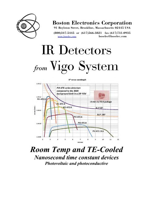
<strong>Boston</strong> <strong>Electronics</strong> <strong>Corporation</strong>91 Boylston Street, Brookline, Massachusetts 02445 USA(800)347-5445 or (617)566-3821 fax (617)731-0935www.boselec.comboselec@boselec.com<strong>IR</strong> <strong>Detectors</strong><strong>from</strong> <strong>Vigo</strong> <strong>System</strong>Room Temp and TE-CooledNanosecond time constant devicesPhotovoltaic and photoconductive
About VIGO <strong>System</strong> S.A.VIGO <strong>System</strong> S.A. is a leading innovator and manufacturer ofuncooled infraredphotodetectors. The companyhas been established tocontinue development andcommercialization of uncooledmiddle and long wavelength <strong>IR</strong>detectors initiated by itsfounders in late 60's at MilitaryUniversity of Technology(Warsaw).Our mission is sensitive, fastconvenient and affordabledetection of <strong>IR</strong> radiation.The devices we develop arebased on unique concept of <strong>IR</strong>detector as device thatintegrates optical, detection andelectronic functions in one monolithic chip device, made ofband-gap engineered structures.At present we manufacture photodetectors optimized for anywavelength within the 2-16 um spectral range. The devices arecharacterized by performance close to the fundamental limitsand sub nanosecond time constants.VIGO <strong>System</strong> S.A. offers products ranging <strong>from</strong> a singleelement photodetectors to integrated detection modulescontaining optics, <strong>IR</strong> detector, coolers, preamplifiers, A/Dconverters and other electronics. We provide also advancedcustom engineering services.The devices have found numerous industrial, scientific,medical, military and other applications.VIGO <strong>System</strong> is located in the high-tech industrial park atOżarów Mazowiecki, western outskirt of Warsaw, Poland. Thecompany owns two buildings with combined 1400 sq. metersof production and office space.VIGO <strong>System</strong> S.A. is ISO 9001 certified.A.P. 25.09.2010Glossary of TermsInfrared <strong>Detectors</strong> <strong>from</strong> VIGO <strong>System</strong> S.A.Hg 1-xCd xTeKnown also as Mercury Cadmium Telluride (MCT), CdHgTe,(Cd,Hg)Te or Mercadtel. Alloy of CdTe and HgTe. Change ofthe CdTe to HgTe ratio (composition or x-value) can be usedto tune optical absorption cut-off wavelength in the wide range<strong>from</strong> UV to deep <strong>IR</strong>. Cooling shifts the cut-off wavelengthtowards long wavelengths. <strong>Detectors</strong> <strong>from</strong> <strong>Vigo</strong> are based oncomplex graded gap MCT structures optimized for MW<strong>IR</strong>(3-5 µm) and LW<strong>IR</strong> (8-14 µm) ranges.Current and Voltage Responsivity: R i, R vcurrent signal d R i=incident power d (in A/W)voltage signald R v=incident power d (in V/W)Current responsivity is typically used for photovoltaicdetectors and voltage responsivity for photoconductors andphotoelectromagnetic detectors.Responsivity - Width ProductThe responsivity of PC and PVM detectors decreases linearlywith increase of the device width (contact width). Thereforethe normalized (area independent) responsivity can beexpressed as the responsivity - width product.Dark Current: I darkIn PV: the current through a photovoltaic cell when the reversebias is applied to its terminals under dark conditions. The darkcurrent is the mainsource of the noisecurrent thatdetermines theminimal detectablesignal.In PC: the currentthrough a biasedphotoconductorwithout the incidentradiant power.Detector FormatsSquare and rectangular formats are used for PC, PEM and PVdevices. Round shapes are also used for some PV devices.Custom shapes are available on request.Maximum Bias Current: I maxThe maximum current that can flow through aphotoconductive or photovoltaic detector without a risk of itsdamage.Multiple Junctions Photovoltaic Devices (PVM)PVM devices are the photovoltaic devices with multiplejunctions connected in series. They are used as large area, longwavelength detectors.Noise: NThe main types of noise are:- Generation-Recombination Noise- Johnson Noise (or Thermal Noise)- Shot Noise- Flicker or 1/f NoiseG-R Noise: Both generation and recombination occurrandomly, resulting in fluctuations in the input current.Johnson Noise or Thermal Noise is caused by thermalagitation of carriers in the conductor. In consequence there israndom fluctuations in the voltage across its terminals.
Shot Noise is due to the discrete nature of radiation, which iscomposed of photons arriving randomly in time. Absorbedphotons produce photoelectrons at random intervals, and thisvariation in current appears as a noise.Flicker or 1/f Noise is a frequency dependent noise that is stillnot fully understood. It occurs in any biased device. Its poweris proportional to 1/ f b where b is approx. 1. Forphotoconductors usually the 1/f knee is in the 1-20 kHz range.For biased LW<strong>IR</strong> photovoltaic detectors 1/f knee is in the 1-10MHz range.Noise Current and Noise Voltage: I n ,V nRoot mean square noise current or voltage.I n =I 2 n t V n =U 2 n tNoise Current and Noise Voltage Density:I ni n= f n= V n fi n , v nNoise Equivalent Power: NEPThe radiant power that produces signal to noise ratio of unity atthe output of the detector per square root bandwidth:NEP= nR v= i nR iinWHzNormalized Detectivity: D*The signal-to-noise ratio (SNR) at a detector output normalizedto 1 W radiant power, a 1 cm 2 detector optical area and a 1 Hzbandwidth. The higher the D* value, the better the detector.D *= R ii nA= R vv nA in cmHz1/2 /WThe D* is related to the NEP: D* = A 1/2 / NEP.The detectivity is the best parameter to characterize detectorsensitivity. The higher the D* the better the detector. The higherperformance can be achieved with optical immersion (Seriesnames with “I”) and thermoelectrical cooling (-2TE, -3TE and-4TE series).Operating Temperature: TBoth room temperature and TE cooled devices are offered. TEcooled devices give better performance but it is also morebulky and need appropriate handling. For more details on TEcooling see the chapter on TE Cooling and Cooler Controllers.Optical Area: AIt is an area where the incident radiant power is collected. Forrectangular photoconductive devices it is a contact width-length product where length is a distance between contacts.Spectral ResponseIt is often understood as a spectral responsivity or a spectraldetectivity. In detector data sheet it is presented as the D*(λ). Itcan be characterized by cut-on, cut-off wavelength, optimumwavelength, and peak wavelength.Optimum Wavelength: λ opThe wavelength for which a device was optimized for. For near<strong>IR</strong> detectors λ op is close to λ peak . In contrast, for uncooled longwavelength detectors λ op can be even larger then λ co . Forexample the uncooled λ op =10.6 µm detector has λ peak =6 to 7µm.Peak Wavelength: λ peakλ peak is a wavelength where a specified device has a maximumresponse.Cut-on and Cut-off Wavelengths: λ con, λ coffλ coff and λ con are minimum and maximum wavelength at whicha detector response reach 50% of the peak value. Cut-on forPC and PVM series is limited by GaAs transmittance (approx.0.9 µm) for MW<strong>IR</strong> single junction photovoltaic detectors cutoffis approx. 2.5 µm and for LW<strong>IR</strong> single junctionphotovoltaic detectors cut-off is approx. 3.5 µm. Customdetectors can be manufactured with different cut-on.Photocurrent: I phThe current signal <strong>from</strong> a photovoltaic device when exposed toincident radiant power. It is described by photovoltaic currentequation:I ph = QA D e gwhere:η - quantum efficiency, Q - photon flux, A d - active area,e - electron load, g - photoelectric gainPhotoelectric Gain: gNumber of electrons passing contacts per one absorbedphoton. In photovoltaic devices g it is close to 1.Photoconductive Devices (PC)Photoconductive Devices (PC) are detectors based onthe photoconductive effect. Infrared radiation generates chargecarriers in the semiconductor active region decreasing itsresistance. The resistance change is sensed as a voltage changeby applying a constant current bias. The optimum bias currentis specified in the Final Test Report and depends on thedetector size, operating temperature and spectralcharacteristics.Photoelectromagnetic Devices (PEM)PEM detectors are photovoltaic devices based onthe photoelectromagnetic effect. It relies on a spatialseparation of optically generated electrons and holes in amagnetic field applied to the semiconductor by a permanentmagnet built in to the detector housing. PEM detectors do notrequire electrical bias and show no flicker (1/f) noise. Thedevices are typically used as fast uncooled detectors of longwavelength radiation.Photovoltaic Devices (PV or PVM)Photovoltaic devices (photodiodes) are semiconductorstructures with one (PV) or multiple (PVM) homo- orheterojunctions. Absorbed photons produce electron-holepairs, resulting in external photocurrent. Reverse bias voltagemay be applied to increase differential resistance, reduce theshot noise, improve high frequency performance and dynamicrange. Reverse bias may increase responsivity in somedevices. Unfortunately, at the expense of flicker (1/f) noise inmost cases. PV detectors are more vulnerable to electrostaticdischarges than photoconductors.Circuitry for Photoconductive <strong>Detectors</strong>A typical circuit for PC MCT detectors is shown in fig. 1a.The detectors are usually low impedance devices and requirelow input voltage noise preamplifiers. A constant bias currentis used in the detector requiring a low noise DC voltage supplyor battery with current-limiting resistor R L . Typically, ACcoupling is used to prevent saturation of the preamplifier bydetector bias.Circuitry for Photovoltaic <strong>Detectors</strong>Transimpedance preamps that provide constant voltage reversebias are required for the best linearity and frequency responseextend high frequency response beyond the unbiased valuespublished in individual VIGO detector data sheets. Consult usfor options. This can be achieved using transimpedanceA.P. 25.09.2010Infrared <strong>Detectors</strong> <strong>from</strong> VIGO <strong>System</strong> S.A.
preamplifiers as shown in the Fig. 1b. This preamplifierprovides also biasing of the detector with DC reverse voltage.In this way, the conditions for a maximum signal-to-noise ratioin a wide waveband are created.R fhν-+V bQuantum Efficiency η:The ratio of the number of generated electron-hole pairs to thenumber of incident photons.Resistance – Area ProductResistance of typical photodiodes (PV series) decreasesproportionally to their area. Therefore the normalize resistancecan be expressed as the R A product.In contrast, the PVM series devices are characterized byconstant sheet resistance.Time constant: τThe time that takes a detector to reach 1/e of the initial signalvalue after switching off the irradiation.Time constant is related to the high frequency cut-off f c (-3dBpoint):=1/2 f c The time constant for one stage low pass RC network can becalculated as proportional to 10-90% rise time t r :t r =2.2Series Resistance: R sParasitic resistance in photodiode. It's contribution to the totaldiode resistance may be significant for long wavelengths andoperating at near room temperatures diodes especially for largeactive area.Sheet Resistance: R sqThe normalized resistance expressed in ohm/square. It is usedto normalize the resistance for different size devices with nonsquareactive areaR sq =Rw/lShunt Resistance: R shThe resistance of the photovoltaic detector biased with zero orvery small voltage (e.g.±10 mV) when not exposed to anyradiation (dark state). Also referred to as dynamic impedance atzero bias.Optimal Wavelength, Spectral RangeTypical spectral responses were presented in the glossary. Ourstandard detectors are detectivity-optimized for any wavelengthwithin 3-16 µm range. Additional optical filters or specialdevice heterostructures can be used to achieve selectivedevices.Frequency responseUncooled and thermoelectrically cooled detectors can be usedfor both low and high frequency applications.Unbiased photovoltaic and photoelectromagnetic detectors arethe devices of choice for operation <strong>from</strong> DC to very highfrequencies, exceeding 1 GHz for some custom devices. Fasterresponse speeds can be obtained by applying reverse bias tophotodiodes. Compare time constant τ and choose the bestsolution for your application.A.P. 25.09.2010Infrared <strong>Detectors</strong> <strong>from</strong> VIGO <strong>System</strong> S.A.
Optical Immersion of the <strong>Detectors</strong>Optical immersion of infrared detectors to high refractionmicrolenses is used to improve performance of the devices butmay limit acceptance angle. Action and properties ofhemispheric and hyperhemispheric lenses are illustrated in thedrawings and tables below.hemispherical lensacceptanceangle Φobjectiveacceptanceangle ΦobjectiveR=Ld – optical (apparent) detector sized' – physical detector sizeR – lens radiusL – lens face to objective focal plane distanceobjectivefocal planed'dhyperhemisphericallensobjectivefocal planeRLd'dApplicationsThe typical applications of the VIGO <strong>System</strong> S.A. detectorsare given in the table below. Please, provide detailed systemrequirements – we will recommend optimum solution.Table 2. ApplicationsApplicationsDetector Series - examplesSpectroscopyPCI-2TE, PVI-nTE, PVI, PCIGas AnalysisPCI-2TE, PVI-nTE, PVI, PCILaser MetrologyPV, PV-2TE, PVM, PVM-2TE,PEM, PEMIHigh Speed OperationPVI-nTE, PVI, PVM, PVMI,PEM, PEMIAnalysis of Spatial and TimeDistribution of Laser BeamPV, PV-nTE, PVM, PVM-nTERemote TemperatureMeasurementsPV-nTE, PVI-nTE, PVI-nTE,PCI, PCI-nTEHeterodyne DetectionPV-2TE, PVI-nTE, PCI,PCI-nTEBiomedical applicationsPV, PVI-nTE, PVM, PVMI,PEM, PEMIPyrometers, ScannersPV-2TE, PVI-nTE, PCI,Thermal ImagersFree Space OpticalCommunicationLIDARDetection and Monitoring ofThermal ObjectsLaser-Matter InteractionStudiesLaser Threat WarningFire, Flame and Human BodyDetectionPositioning <strong>System</strong>sTracking <strong>System</strong>sNondestructive MaterialTestingPCI-nTEPV-2TE, PVI-nTE, PCI,PCI-nTEPVI-nTE, PVIPVI-nTE, PCI-nTEPV-2TE, PVI-nTE PCI,PCI-nTEPV, PV-2TE, PVM, PVM-2TE,PEM, PEMIMPC, PCI, PVI, PVMIPV-2TE, PVI-nTE, PCI,PCI-nTEPV, PV-2TEPV, PV-2TE, PC, PCI,PCI-2TE, PC-2TEAll DevicesTable 1. Immersed device parametersParameter Hemisphere HyperhemisphereTheory GaAs Theory GaAsDistance, L R R R(n + 1) 4.3Rd/d' n 3.3 n 2 10.9D* imm /D* nonimm n 3.3 n 2 10.9Acceptance angle, Φ 180˚ 180˚ 2 arcsin(1/n) 35F/# 0.5 0.5 n/2 1.62Where n is the index of refraction (~3.3 for GaAs)The values in table 1 show the relative change of a givenparameter comparing to a non-immersed detector of the sameoptical size.<strong>Detectors</strong> with custom acceptance angles are available onrequest.Immersion technology is described in “Infrared <strong>Detectors</strong> and<strong>System</strong>s”, E.L. Dereniak and G.D. Boreman, WileyInterscience 2000.A.P. 25.09.2010Infrared <strong>Detectors</strong> <strong>from</strong> VIGO <strong>System</strong> S.A.
Custom Engineering25 years of experience in infrared technology has given usopportunity to provide the extensive custom engineeringcapabilities. Our Custom Engineering staff is ready for closecooperation with our partners at any stage of the developmentprocess to select the best solutions.Our manufacturing technologies are very flexible, therefore inaddition to our catalog products, we could offer optimizeddevices for particular applications- various detector areas andformats, spectral and frequency response, temperature ofoperation, field of view, packages, connectors and othercharacteristics. Custom detector formats available at present areshaped single element detectors, linear and bilinear arrays,small 2-D arrays (e.g. quadrants).Even more flexible are integrated optics /detector/electronicspackages, fabricated for general use and OEM applications.They may include objectives, optical filters, detectors, variouspreamplifiers, detector bias circuits, A/D converters, Peltiercoolers, cooler controllers, heat dissipation and othercomponents.Quadrant Detector in a Specialised PackageStandard PackagesMultielement Linear ArrayEpitaxial Production <strong>System</strong>A.P. 25.09.2010Infrared <strong>Detectors</strong> <strong>from</strong> VIGO <strong>System</strong> S.A.
Comparison tableUncooled detectors without optical immersionModel λ op, μm Type D*, cmHz 1/2 /W τ, nsPV-3 3 PV 6.5×10 9 15PV-3.4 3.4 PV 5×10 9 15PC-4 4 PC 2×10 9 1000PV-4 4 PV 3×10 9 15PC-5 5 PC 1×10 9 500PV-5 5 PV 1×10 9 15PC-6 6 PC 3×10 8 200PV-6 6 PV 5×10 8 12PV-8 8 PV 4×10 7 7PVM-8 8 PV 6×10 7 12PC-9 9 PC 2×10 7 2PC-10.6 10.6 PC 9×10 6 1PVM-10.6 10.6 PV 1×10 7 1PEM-10.6 10.6 PEM 1×10 7 1PCQ-10.6 10.6 PC 9×10 6 12TE cooled optically immersed detectorsModel λ op, μm Type D*, cmHz1 /2 /W τ, nsPVI-2TE-3 3 PV 5.5×10 11 15PVI-2TE-3.4 3.4 PV 3×10 11 15PCI-2TE-4 4 PC 4×10 10 4000PVI-2TE-4 4 PV 2×10 11 20PCI-2TE-5 5 PC 2×10 10 2000PVI-2TE-5 5 PV 6×10 10 20PCI-2TE-6 6 PC 1×10 10 1000PVI-2TE-6 6 PV 2×10 10 10PVI-2TE-8 8 PV 2×10 9 7PVMI-2TE-8 8 PV 2×10 9 3PCI-2TE-9 9 PC 4×10 9 7PCI-2TE-10.6 10.6 PC 1.4×10 9 3PVI-2TE-10.6 10.6 PV 1×10 9 3PVMI-2TE-10.6 10.6 PV 1×10 9 3PCI-2TE-12 12 PC 4.5×10 8 2PCI-2TE-13 13 PC 2.3×10 8 2Uncooled optically immersed detectorsModel λ op, μm Type D*, cmHz 1/2 /W τ, nsPVI-3 3 PV 5×10 10 15PVI-3.4 3.4 PV 4.5×10 10 15PCI-4 4 PC 6×10 9 1000PVI-4 4 PV 2×10 10 15PCI-5 5 PC 4×10 9 500PVI-5 5 PV 5×10 9 15PCI-6 6 PC 1×10 9 200PVI-6 6 PV 4×10 9 12PVI-8 8 PV 4×10 8 7PVMI-8 8 PV 3×10 8 7PCI-9 9 PC 1×10 8 2PCI-10.6 10.6 PC 9×10 7 1PVMI-10.6 10.6 PV 1×10 8 1PEMI-10.6 10.6 PEM 5×10 7 12TE cooled detector without optical immersionModel λ op, μm Type D*, cmHz 1/2 /W τ, nsPV-2TE-3 3 PV 7×10 10 15PV-2TE-3.4 3.4 PV 4×10 10 15PC-2TE-4 4 PC 2×10 10 4000PV-2TE-4 4 PV 3×10 10 20PC-2TE-5 5 PC 1×10 10 2000PV-2TE-5 5 PV 9×10 9 20PC-2TE-6 6 PC 3×10 9 1000PV-2TE-6 6 PV 2×10 9 10PV-2TE-8 8 PV 2×10 8 7PVM-2TE-8 8 PV 3×10 8 7PC-2TE-9 9 PC 4.5×10 8 7PC-2TE-10.6 10.6 PC 1.4×10 8 3PV-2TE-10.6 10.6 PV 1×10 8 3PVM-2TE-10.6 10.6 PV 1×10 8 3PC-2TE-12 12 PC 4.5×10 7 2PC-2TE-13 13 PC 9×10 6 2A.P. 25.09.2010Infrared <strong>Detectors</strong> <strong>from</strong> VIGO <strong>System</strong> S.A.
3TE cooled optically immersed detectorsModel λ op, μm Type D*, cmHz 1/2 /W τ, nsPVI-3TE-3 3 PV 7×10 11 15PVI-3TE-3.4 3.4 PV 5×10 11 15PVI-3TE-4 4 PV 4×10 11 20PVI-3TE-5 5 PV 8×10 10 20PVI-3TE-6 6 PV 3×10 10 10PVI-3TE-8 8 PV 3×10 9 7PVMI-3TE-8 8 PV 3×10 9 7PCI-3TE-9 9 PC 6×10 9 8PCI-3TE-10.6 10.6 PC 2.5×10 9 5PVI-3TE-10.6 10.6 PV 1.5×10 9 3PVMI-3TE-10.6 10.6 PV 2.5×10 9 7PCI-3TE-12 12 PC 9×10 8 5PCI-3TE-13 13 PC 4.5×10 8 4λ op , μm – Optimal wavelength - The wavelength for which adevice was optimized for. For near <strong>IR</strong> detectors λ op is close topeak value. In contrast, for uncooled (300K) long wavelengthdetectors λ op is larger is than λ co .Device type:PC – Photoconductive,PV- Photovoltaic,PEM – PhotoelectromagneticD*, cmHz ½ /W – minimum detectivity. The higher the D*value, the better the detector.τ, ns - maximum time constant (“1/e” time)Time constants have been measured using Alpes Lasers SAquantum cascade lasers (QCL) (www.alpeslasers.ch).3TE cooled detectors without optical immersionModel λ op, μm Type D*, cmHz 1/2 /W τ, nsPV-3TE-3 3 PV 1×10 11 15PV-3TE-3.4 3.4 PV 7×10 10 15PV-3TE-4 4 PV 4×10 10 20PV-3TE-5 5 PV 1×10 10 20PV-3TE-6 6 PV 4×10 9 10PV-3TE-8 8 PV 3×10 8 7PV-3TE-10.6 10.6 PV 1.5×10 8 3PC-3TE-9 9 PC 1.5×10 9 8PC-3TE-10.6 10.6 PC 2.5×10 8 5PC-3TE-12 12 PC 9×10 7 5PC-3TE-13 13 PC 6×10 7 44TE cooled detectorsModel λ op, μm Type D*, cmHz 1/2 /W τ, nsPV-4TE-3 3 PV 1.5×10 11 15PV-4TE-3.4 3.4 PV 1×10 11 15PV-4TE-4 4 PV 6×10 10 20PV-4TE-5 5 PV 1.5×10 10 20PV-4TE-6 6 PV 5×10 9 10PV-4TE-8 8 PV 4×10 8 7PV-4TE-10.6 10.6 PV 2×10 8 3PVI-4TE-3 3 PV 8×10 11 15PVI-4TE-3.4 3.4 PV 7×10 11 15PVI-4TE-4 4 PV 4×10 11 20PVI-4TE-5 5 PV 1×10 11 20PVI-4TE-6 6 PV 4×10 10 10PVI-4TE-8 8 PV 4×10 9 7PVI-4TE-10.6 10.6 PV 2×10 9 3A.P. 25.09.2010Infrared <strong>Detectors</strong> <strong>from</strong> VIGO <strong>System</strong> S.A.
Packages, Windows and Pin LayoutDevices are delivered in several packages: TO-8, BNC-based,TO-39, PEM with SMA connectors and quadrant with SMAconnectors. The BNC and the TO-39 packages are used foruncooled PV and PC devices. The TO-8 package is used for TEcooled devices. All TE-cooled detectors are provided with awindow. We offer windows optimized for different spectralbands: BaF 2 , ZnSe, CdTe, CaF 2 , sapphire, Si and Ge. Windowscan be anti reflection coated upon request.TO-39 PackagesWindowless TO-39-based packages are typically used foruncooled devicesPEM Specialized PackagesDimensions in millimeters.The photoelectromagnetic detectors (PEMI-, PEM-) aremounted in specialized packages with SMA connectors,designed for broadband applications. A magnetic circuit isincorporated into the package.BaF 2 window is supplied as astandard. Dimensions in millimeters.Signal 1(+), 2(-), 3 (GND)Detectoroptical area[mm 2 ]Hyperhemisphere0.5×0.5 1×1 2×2 3×3Hemisphere0.5×0.5 –3×3Flat0.01×0.01– 4×4R [mm] 0.5 0.8 1.25 1.6 0.5-1.6 ∞A [mm] 1.5±0.2 2.4±0.2 3.75±0.2 4.8±0.2 0 0B [mm] 1.9±0.2 1.9±0.2 1.9±0.2 1.9±0.2 1.9±0.2 1.9±0.2FOV ~36º ~36º ~36º ~36º ~90º ~90ºA.P. 25.09.2010Infrared <strong>Detectors</strong> <strong>from</strong> VIGO <strong>System</strong> S.A.
TO-8 PackagesThe TO-8-based packages are used for thermoelectricallycooled devices (PC-nTE, PCI-nTE, PV-nTE, PVM-nTE andPVI-nTE). The packages are filled with dry, heavy gases forlow thermal conductivity (Kr/Xe mixtures). Water vaporcondensation is prevented by careful sealing and waterabsorbers applied inside the package. BaF 2 windows are usedas a standard, other windows possible on request. Dimensionsin millimeters.4TEHyperhemisphere Hemisphere FlatOptical0.5×0.5 – 0.01×0.00.5×0.5 1×1 2×2 3×3area[mm 2 ]3×3 1 – 4×4R [mm] 0.5 0.8 1.25 1.6 0.5-1.6 ∞A [mm] 7.3±0.4 6.4±0.4 5±0.4 4±0.48.8±0.4 8.8±0.4B [mm] 8.8±0.4 8.8±0.4 8.8±0.4 8.8±0.48.8±0.4 8.8±0.4C [mm] 14±0.3 14±0.3 14±0.3 14±0.314±0.3 14±0.3FOV ~36° ~36° ~36° ~36° ~70º ~70ºbottom v iew – pin lay out9 10 11 12 1Packages with BNC ConnectorsThe specialized BNC-based packages are used for uncooledroom temperature devices (MPC, PC, PCI, PV, PVI, PVM,PVMI). Standard devices are delivered without a window.Dimensions in millimeters.8I Ph276543Signal 1 and 3Thermistor7 and 9TE Cooler Supply2(+) and 8(-)Chassis Ground11not used 4, 5, 6, 10, 12Note: 2-56UNC-2A thread: 56 threads/inch, major dia.: 0.086”,minor dia.: 0.0648”, pitch dia.: 0.0744”2TEHyperhemisphere Hemisphere FlatOpticalarea[mm 2 ] 0.5×0.5 1×1 2×2 3×3 0.5×0.5 – 0.01×0.03×3 1 – 4×4R [mm] 0.5 0.8 1.25 1.6 0.5-1.6 ∞A [mm] 4.1±0.3 3.2±0.3 1.85±0.3 0.8±0.3 5.6±0.3 5.6±0.3B [mm] 5.6±0.3 5.6±0.3 5.6±0.3 5.6±0.3 5.6±0.3 5.6±0.3C [mm] 11±0.3 11±0.3 11±0.3 11±0.3 11±0.3 11±0.3FOV ~36° ~36° ~36° ~36° ~70º ~70º3TEHyperhemisphere Hemisphere FlatOpticalArea[mm] 0.5×0.5 1×1 2×2 3×3 0.5×0.5 – 0.01×0.03×3 1 – 4×4R [mm] 0.5 0.8 1.25 1.6 0.5-1.6 ∞A [mm]5.7±0.3 4.8±0. 3.45±0.3 2.4±0.35 35 5 57.2±0.35 7.2±0.35B [mm]7.2±0.3 7.2±0.7.2±0.35 7.2±0.35 3557.2±0.35 7.2±0.35C [mm]12.4±0. 12.4±012.4±0.3 12.4±0.3 .3312.4±0.3 12.4±0.3FOV ~36º ~36º ~36º ~36º ~70º ~70ºUncooledHyperhemisphere Hemisphere FlatOptical0.5×0.5 – 0.01×0.010.5×0.5 1×1 2×2 3×3area3×3 – 4×4R [mm] 0.5 0.8 1.25 1.6 0.5-1.6 ∞A [mm] 4.6±0.3 5.5±0.3 6.85±0.3 7.9±0.3 3.1±0.3 1.6±0.3B [mm] 3.1±0.1 3.1±0.15 53.1±0.15 3.1±0.15 3.1±0.15 1.6±0.15FOV,C=Ø4~36° ~36° ~36° ~36° 66° 102°FOV,C=Ø6~36° ~36° ~36° ~36° 88° 124°A.P. 25.09.2010Infrared <strong>Detectors</strong> <strong>from</strong> VIGO <strong>System</strong> S.A.
Quadrant PackagesDevices are mounted in specially designed packages, suppliedwith the SMA connectors, suitable for fast applications. Thesepackages are used for PCQ, PVQ and PVMQ devices.Standard devices are delivered without a window.Dimensions in millimeters.TO-8 Quadrant PackagesOther option is package based on TO-8 headers, suitable forfast applications and PCB soldering. These packages are usedfor PCQ, PVQ and PVMQ devices.Standard devices are delivered without a window.Dimensions in millimeters.A.P. 25.09.2010Infrared <strong>Detectors</strong> <strong>from</strong> VIGO <strong>System</strong> S.A.
TE coolingCooling reduces noise, increases responsivity and, in somedevices, improves high frequency response.The devices with two, three and four stage TE coolers areavailable as a standard. TE cooler (TEC) is biased with the DCpower. Performance data shown in specifications is given forheat sink temperature 300K. The coolers are characterized by:Maximum temperature difference ΔT maxΔT max rated at Q=0, at other Q the ΔT should be estimated asΔT=ΔT max (1-Q/Q max )Optimum current: I optCurrent resulting the highest temperature difference (ΔT max ) atthe specified conditions stated in test data sheet for eachdetector.Maximum TEC current: I maxCurrent resulting in greatest ΔT max without the heat load. . Thehigher currents may damage the cooler. To ensure lastingoperation it is recommended to supply the cooler with
Precautions for UseStorageThe following conditions should be fulfilled for the safe andreliable operation of detectors:-Storage temperature: -10ºC to +50ºC-Avoiding ESD; detectors are very sensitive to electrostaticdischarges, therefore they should be stored having detectionelement’s leads shorted.HandlingWindows of some detectors are made of very soft materialslike ZnSe or BaF 2 . Particular attention should be paid to notscratch a surface of the window when some sharp tools are inuse. A damaged window may entirely degrade the detector’sperformance. Excessive mechanical stress applied to thepackage itself or to a device containing the package may resultin permanent damage of the latter.Beam Power LimitationsFor devices without immersion lens continuous work incidentbeam power must not exceed 100 W/cm 2 and pulses shorterthan 1 µs must not exceed 1 MW/cm 2 .For optically immersed devices continuous work incident beampower must not exceed 2.5 W/cm 2 and pulses shorter than 1 µsmust not exceed 10 kW/cm. Stated power densities arespecified at λ opt . Saturation power density depends on a type ofthe detector and can be provided upon request.Shaping LeadsAvoid bending the leads at a distance less then 2 mm <strong>from</strong> abase of the package to prevent glass seals damage. Whenshaping the leads, do not exceed the following limits:- Maximal mechanical tension – 0.5 kg for 5 sec- Maximum two right angle bends and three twists at thedistance minimum 6 mm <strong>from</strong> the base of the packageWhen shaping the leads of the detector, short the leads of thedetecting element.Soldering Leads<strong>IR</strong> <strong>Detectors</strong> can be easily damaged by excessive heat. Specialcare should be taken when soldering the leads. Usage of heatsinks is highly recommended. Tweezers can be used for thispurpose; when soldering clamp a lead at a place between thesoldering iron and the base of the case. To avoid destructiveinfluence of ESD and other accidental voltages (deriving forexample <strong>from</strong> a non-grounded soldering iron) all rules forhandling LSI integrated circuits should be applied to <strong>IR</strong>detectors too.Cleaning WindowKeep the window clean. Use a soft cotton cloth damped withisopropyl alcohol and wipe off the surface gently if necessary.Mechanical ShocksThe Peltier elements may be damaged by the excessivemechanical shocks and vibrations. Great care is recommendedduring all manipulations (including normal exploitation) toavoid the mentioned hazards. Drop impacts against a hard basemay be particularly dangerous.Heat SinkingThe base of the detector housing must be firmly attached to theheat sink. This can be achieved either by using a thin layer ofheat conductive epoxy glue or silicone grease between thementioned elements. The latter requires carefully madeclamping of the elements to assure possibly thin layer of thegrease.WarrantyVIGO <strong>System</strong> S.A. issues a warranty for the material and theworkmanship of its products under normal operatingconditions for the period of one year <strong>from</strong> the date of thedelivery. Exceptional operating conditions, damage due tocareless handling and misapplication may void the warranty.A.P. 25.09.2010Infrared <strong>Detectors</strong> <strong>from</strong> VIGO <strong>System</strong> S.A.
Part numberingType Immersion - Cooling - λ op - Length x Width - Pack Type - Window - FOVType Immersion - Cooling - λ op - Φ Diameter - Pack Type - Window - FOVI) PVI-2TE-5-0.1x0.1-TO8-BaF2-35PV I - 2TE - 5 - 0.1 x 0.1 - TO8 - BaF2 - 352) PEM-10.6-1x1-PEM-NO WINDOWPVM - - 10.6 - 1 x 1 - PEM - NO WINDOW -3) PC-10.6-1x1-BNC-NO WINDOWPC - - 10.6 - 1 x 1 - BNC - NO WINDOW -4) PVI-2TE-6-ø0.05-TO8-ARGe-60PV I - 2TE - 6 - Φ 0.05 - TO8 - ARGe - 60Types:PC – PhotoconductorsPV – Single Junction Photovoltaic DevicesPVM – LW<strong>IR</strong> Multiple Junction Photovoltaic Devices optimized for large areaPEM – Photoelectromagnetic DevicesPCQ – Quadrant PhotoconductorsImmersion:All devices can be monolithically integrated with optical immersion lens. Add letter 'I' to the end of type symbol for immerseddetectors. Hiperhemispherical immersion is offered as a standardCooler TypeOur PC, PV and PVM detectors are available as uncooled devices or equipped with multiple stage TE cooling. Add '-2TE','-3TE' or '-4TE' for two, three or four stage TE cooled devices.Wavelength Range and Optimum Wavelength (λ op):Our standard devices are optimized for specific wavelength see table below. Other wavelength are available as an option.TypeOptimum WavelengthPC, PCI 4 5 6 9 10.6PC-2TE, PCI-2TE 4 5 6 9 10.6 12 13PV, PVI 3 3.4 4 5 6 8PV-2TE, PVI-2TE, PVI-3TE 3 3.4 4 5 6 8 10.6PCI-3TE 10.6 12 13PVM, PVMI, PVMI-2TE 8 10.6PVM-2TE, PEM, PEMI, PCQ 10.6Optical Area availability tableTypical devices are square-shaped. Single junction photovoltaic devices are also available as a circular. Specify side length anddiameter for square and circular areas, respectively.TypeLength or diameter [mm]0.025 0.05 0.1 0.2 0.25 0.5 1 2 3 4MPC X X X XPV-3 O X X O O OPV-2TE-3 O X X O O OPV-3TE-3 O X X O O OPV-4TE-3 O X X O O OPVI-3 O X X OPVI-2TE-3 O X X OPVI-3TE-3 O X X OPVI-4TE-3 O X X OPV-3.4 O X X O O OPV-2TE-3.4 O X X O O OPV-3TE-3.4 O X X O O OPV-4TE-3.4 O X X O O OPVI-3.4 O X X OPVI-2TE-3.4 O X X OPVI-3TE-3.4 O X X OPVI-4TE-3.4 O X X OPC-4 X X X X X X X X X XPC-2TE-4 X X X X X X X XPCI-4 X X X XPCI-2TE-4 X X X XPV-4 O X X O O OPV-2TE-4 O X X O O OPV-3TE-4 O X X O O OPV-4TE-4 O X X O O OPVI-4 O X X OPVI-2TE-4 O X X OPVI-3TE-4 O X X OPVI-4TE-4 O X X OPC-5 X X X X X X X X X XA.P. 25.09.2010Infrared <strong>Detectors</strong> <strong>from</strong> VIGO <strong>System</strong> S.A.
TypeLength or diameter [mm]0.025 0.05 0.1 0.2 0.25 0.5 1 2 3 4PC-2TE-5 X X X X X X X XPCI-5 X X X XPCI-2TE-5 X X X XPV-5 O X X O O OPV-2TE-5 O X X O O OPV-3TE-5 O X X O O OPV-4TE-5 O X X O O OPVI-5 O X X OPVI-2TE-5 O X X OPVI-3TE-5 O X X OPVI-3TE-5 O X X OPVI-4TE-5 O X X OPC-6 X X X X X X X X X XPC-2TE-6 X X X X X X X XPCI-6 X X X XPCI-2TE-6 X X X XPV-6 O X X O O OPV-2TE-6 O X X O O OPV-3TE-6 O X X O O OPV-4TE-6 O X X O O OPVI-6 O O X OPVI-2TE-6 O X X OPVI-3TE-6 O X X OPVI-4TE-6 O X X OPV-8 X X* PPV-2TE-8 X X* PPV-3TE-8 X X* PPV-4TE-8 X X* PPVI-8 X X X* PPVI-2TE-8 X X X* PPVI-3TE-8 X X X* PPVI-4TE-8 X X X* PPVM-8 O O X X O O X X X XPVM-2TE-8 O O X X O O X X XPVMI-8 O O O X XPVMI-2TE-8 O O X X O O X XPC-9 X X X X X X X X X XPC-2TE-9 X X X X X X X XPC-3TE-9 X X X X X X X XPCI-9 X X X XPCI-2TE-9 X X X XPCI-3TE-9 X X X XPC-10.6 (R005) X X X X X X X X X XPC-2TE-10.6 X X X X X X X XPC-3TE-10.6 X X X X X X X XPCI-10.6 X X X XPCI-2TE-10.6 X X X XPCI-3TE-10.6 X X X XPV-2TE-10.6 X X* PPV-3TE-10.6 X X* PPV-4TE-10.6 x X* PPVI-2TE-10.6 X X X* PPVI-3TE-10.6 X X X* PPVI-4TE-10.6 X X X* PPVM-10.6 O O X X O O X X X XPVM-2TE-10.6 O O X X O O X X XPVMI-10.6 O O X XPVMI-2TE-10.6 O O X XPVMI-3TE-10.6 O O X XPEM-10.6 O O O O X XPEMI-10.6 O O X XPCQ-10.6 X X X X X X X X XPC-2TE-12 X X X X X X X XPC-3TE-12 X X X X X X X XPCI-2TE-12 X X X XPCI-3TE-12 X X X XPC-2TE-13 X X X X X X X XPC-3TE-13 X X X X X X X XPCI-2TE-13 X X X XPCI-3TE-13 X X X X*) Devices may require reverse bias in order to increase dynamic resistance and improve frequency response.X – standard device without bias, P – default with reverse bias , O – detectors available on request, parameters may vary <strong>from</strong> these in data sheets.Package Type (Pack_Type):Devices are typically offered in 5 different packages:TypePC,PCI, PV, PVI, PVM, PVMIPC-2TE,PCI-2TE, PV-2TE, PVI-2TE, PVM-2TE, PVMI-2TE, PCI-3TE, PVI-3TE, PVI-4TE,PEM, PEMIPCQPack_TypeBNC, TO39Window Type (Window):Cooled devices are typically offered with wedged BaF 2 window. When no window is needed, "NO WINDOW" attribute mustbe added. Windows are available as following options:Window Symbol Window SymbolBaF 2 BaF2 sapphire Al2O3ZnSe ZnSe AR-coated Si ARSiCdTe CdTe AR-coated Ge ARGeCaF 2 CaF2FOV - Field of View:Angular field of view of detector in degrees. Depends on type of immersion lens applied and package used for the detector.DatasheetsTO8PEMPCQA.P. 25.09.2010Infrared <strong>Detectors</strong> <strong>from</strong> VIGO <strong>System</strong> S.A.
MPC SERIESMULTISPECTRAL <strong>IR</strong> PHOTOCONDUCTORSAMBIENT TEMPERATURE101Rv , V/W0.10.01λ, µm0 1 2 3 4 5 6 7 8 9 10 11 12 13 14FEATURES- 0.5-12 µm spectral range- D*(1.06 µm) up to 3×10 7 cmHz 1/2 /W- D*(10.6 µm) up to 9×10 6 cmHz 1/2 /W- 1 ns time constant @ 10.6µm- Sheet resistance 30-70 Ohm/sq- High output signal- Perfect match to fast electronics- Lightweight, rugged and reliable- Convenient to use- Low cost- Custom design upon requestDESCRIPTIONSpectral response optimized for maximum performance at twowavelengths 1.06 and 10.6 µm. Devices are typically mounted inmodified TO-39-style packages with ZnSe windows or without anywindow. Specialized packages with other connectors and windowsare available upon request.See application notes for more details.Length or diameter [mm]Type0.025 0.05 0.1 0.2 0.25 0.5 1 2 3 4MPC X X X XACCESSORIESStand Alone Preamplifier/SupplyIntegrated Preamplifier/SupplyVIGO <strong>System</strong> S.A.Polandinfo@vigo.com.plAgents: <strong>Boston</strong> <strong>Electronics</strong> <strong>Corporation</strong>91 Boylston St.Brookline MA 02445 USAirdet@boselec.com www.boselec.comA.P. 25.09.2010Infrared <strong>Detectors</strong> <strong>from</strong> VIGO <strong>System</strong> S.A.
PC SERIES2-11 µm <strong>IR</strong> PHOTOCONDUCTORS1E+101E+91E+8D*, cmHz1/2/WPC-4PC-5PC-6PC-91E+7PC-10.6FEATURES- Ambient temperature operation- Wide dynamic range- Perfect match to fast electronics- Convenient to use- Low cost- Prompt delivery- Custom design upon requestSPECIFICATIONDESCRIPTIONThe PC-n (where n is wavelength λ op in micrometers, to whichthe detector is optimized) series are high speed, ambienttemperature photoconductive mode <strong>IR</strong> photodetectors. Thesedevices can be optimized for the maximum performanceanywhere <strong>from</strong> 2 to 11 µm. High performance and stability wereachieved by using band gap engineered (HgCdZn)Te structureswith optimized composition/doping profiles and improvedsurface processing. They are housed in rugged packages ofreduced size and weight. Performance data are provided witheach detector.The detectors are well suited for heterodyne detection due to avery short time constant and to the perfect match to fastelectronics.Custom devices with quadrant cells, multielement arrays,specialized packages, connectors, windows and optical filtersare available on request.@20ºCCHARACTERISTICS UNITS PC-4 PC-5 PC-6 PC-9 PC-10.6λ op µm 4 5 6 9 10.6Detectivity*:at λ peak, 20kHzat λ op, 20kHzcmHz 1/2 /W >3.2×10 9 >1.5×10 9 >7×10 8 >1×10 8 >1.9×10 7>2×10 9 >1×10 9 >3×10 8 >2×10 7 >9×10 6Responsivity-Widthproduct @ λ opVmm/W >100 >40 >6 >0.4 >0.1Time Constant ns
PC-2TESERIES2-13 μm <strong>IR</strong> PHOTOCONDUCTORSTHERMOELECTRICALLY COOLED1E+111E+101E+9D*, cmHz1/2/WPC-2TE-4PC-2TE-5PC-2TE-6PC-2TE-9PC-2TE-10.61E+8PC-2TE-121E+7PC-2TE-13λ, µm1 2 3 4 5 6 7 8 9 10 11 12 13 14FEATURES- High performance in the 2 to 13 µm range- Fast response- Convenient to use- Wide dynamic range- Compact, rugged and reliable- Low cost- Prompt delivery- Custom design upon requestSPECIFICATIONDESCRIPTIONThe PC-2TE-n (where n is wavelength λ op , in µm, to which thedetector is optimized) series photodetectors are two-stage TEcooled<strong>IR</strong> photoconductive detectors. These devices can beoptimized for the maximum performance anywhere within 2 to 13µm range. High performance and stability were achieved by usingband gap engineered (HgCdZn)Te structures with optimized dopingand improved surface processing. Custom devices with quadrantcells, multielement arrays, various immersion lenses, windows andoptical filters are available on request.Standard detectors are available in modified TO-8 packages withBaF 2 windows. Other packages, windows and connectors areavailable upon request. See application notes for more details.@20ºCCHARACTERISTICS UNITS PC-2TE-4 PC-2TE-5 PC-2TE-6 PC-2TE-9 PC-2TE- PC-2TE- PC-2TE-10.6 12 13λ op µm 4 5 6 9 10.6 12 13Detectivity*:at λ peak, 20kHzat λ op, 20kHzcmHz 1/2 /W >3.2×10 10>2×10 10 >2×10 10>1×10 10 >6×10 9>3×10 9 >9×10 8>4.5×10 8 >4×10 8>1.4×10 8 >1×10 8>4.5×10 7 >4×10 7>2×10 7Responsivity-Width product @λ op 1x1 mmVmm/W >1000 >500 >70 >5 >1.5 >0.5 >0.25Time Constant ns
PC-3TE SERIES1E+101E+92-14 µm <strong>IR</strong> PHOTOCONDUCTIVEDETECTORS THERMOELECTRICALLY COOLEDD*, cmHz1/2/WPC-3TE-9PC-3TE-10.61E+8PC-3TE-13PC-3TE-121E+7λ, µm1 2 3 4 5 6 7 8 9 10 11 12 13 14FEATURES- High performance in the 2-14 µm range- Fast response- Convenient to use- Wide dynamic range- Compact, rugged and reliable- Low cost- Prompt delivery- Custom design upon requestSPECIFICATIONDESCRIPTIONThe PC-3TE-n (where n is wavelength λ op , in micrometers, to which thedetector is optimized) series photodetectors are three-stage TE-cooled <strong>IR</strong>photoconductive detectors. These devices can be optimized for themaximum performance anywhere within 2 to 14 µm range. Highperformance and stability were achieved by using band gap engineered(HgCdZn)Te structures of optimized doping and improved surfaceprocessing. Custom devices with quadrant cells, multielement arrays,various immersion lenses, windows and optical filters are available onrequest. Standard detectors are available in modified TO-8 packageswith BaF 2 windows. Other packages, windows and connectors areavailable upon request. See application notes for more details.@20ºCCHARACTERISTICS UNITS PC-3TE-9 PC-3TE-10.6 PC-3TE-12 PC-3TE-13λ op µm 9 10.6 12 13Detectivity*:at λ peak, 20kHzat λ op, 20kHzcmHz 1/2 /W ≥2.9×10 9 ≥4.5×10 8 ≥1.8×10 8 ≥1.2×10 8≥1.5×10 9 ≥2.5×10 8 ≥9×10 7 ≥6×10 7Responsivity-Width product @λ op1×1 mmVmm/W ≥15 ≥3 ≥1.5 ≥1Time Constant ns
PCI SERIES2-11 µm <strong>IR</strong> PHOTOCONDUCTORSOPTICALLY IMMERSED1E+111E+101E+9D*, cmHz1/2/WPCI-4PCI-5PCI-6PCI-91E+8PCI-10.6FEATURES- Ambient temperature operation- Time constant of 1 ns or less- Wide dynamic range- Perfect match to fast electronics- Convenient to use- Low cost- Prompt delivery- Custom design upon requestSPECIFICATIONDESCRIPTIONThe PCI-n (where n is wavelength λ op , in micrometers, to whichthe detector is optimized) series photodetectors are uncooled <strong>IR</strong>photoconductors, which have been optically immersed to highrefractive index GaAs hyperhemispherical (standard) orhemispherical (option) lenses. These devices can be optimizedfor the maximum performance anywhere within 2 to 11 µmrange. High performance and stability were achieved by using aband gap engineered (HgCdZn)Te, structures with optimizedcomposition/doping profiles and improved surface processing.Custom devices with quadrant cells, multielement arrays,specialized packages, connectors, windows and optical filtersare available on request.@20ºCCHARACTERISTICS UNITS PCI-4 PCI-5 PCI-6 PCI-9 PCI-10.6λ op µm 4 5 6 9 10.6Detectivity*:at λ peak, 20kHzat λ op, 20kHz1 2 3 4 5 6 7 8 9 10 11 12cmHz 1/2 /W >1×10 10 >8×10 9 >2.5×10 9 >5×10 8 >1×10 8>6×10 9 >4×10 9 >1×10 9 >1×10 8 >8×10 7Responsivity-Width product @λ op 1x1 mmVmm/W >600 >300 >60 >3 >1Time Constant ns
PCI-2TE SERIES2-14 μm <strong>IR</strong> PHOTOCONDUCTORSTHERMOELECTRICALLY COOLEDOPTICALLY IMMERSED1E+111E+10D*, cmHz1/2/WPCI-2TE-4PCI-2TE-5PCI-2TE-6PCI-2TE-9PCI-2TE-10.61E+91E+8PCI-2TE-12PCI-2TE-13λ, µm1 2 3 4 5 6 7 8 9 10 11 12 13 14FEATURES- High performance in the 2 to 14 µm range- Fast response- Convenient to use- Wide dynamic range- Compact, rugged and reliable- Low cost- Prompt delivery- Custom design upon requestSPECIFICATIONDESCRIPTIONThe PCI-2TE-n (where n is wavelength λ op , in micrometers, to whichthe detector is optimized) series photodetectors are two-stage TEcooled<strong>IR</strong> photoconductive detectors, which have been opticallyimmersed to high refractive index GaAs hyperhemispherical(standard) or hemispherical (option) lenses. These devices can beoptimized for the maximum performance anywhere within 2 to 14µm range. High performance and stability were achieved by usingband gap engineered (HgCdZn)Te structures of optimized doping andimproved surface processing. Custom devices with quadrant cells,multielement arrays, various immersion lenses, windows and opticalfilters are available on request.Standard detectors are available in modified TO-8 packages withBaF 2 windows. Other packages, windows and connectors areavailable upon request. See application notes for more details.@20ºCUNITS PCI-2TE-4 PCI-2TE-5 PCI-2TE-6 PCI-2TE- PCI-2TE- PCI-2TE- PCI-2TE-CHARACTERISTICS9 10.6 12 13λ op µm 4 5 6 9 10.6 12 13Detectivity*:cmHzat λ peak, 20kHz1/2 />6×10W10 >4×10 10 >2×10 10 >1×10 10 >3.5×10 9 >1×10 9 >4×10 8at λ op, 20kHz>4×10 10 >2×10 10 >1×10 10 >4×10 9 >1.4×10 9 >4.5×10 8 >2.3×10 8Responsivity-W idth product@λ op 1x1mmVmm/W >6000 >3000 >600 >40 >15 >5 >2.5Time Constant ns
PCI-3TE SERIES2-14 µm <strong>IR</strong> PHOTOCONDUCTIVEDETECTORS THERMOELECTRICALLY COOLEDOPTICALLY IMMERSED1E+111E+10D*, cmHz1/2/WPCI-3TE-9PCI-3TE-10.61E+9PCI-3TE-13PCI-3TE-121E+8λ, µm1 2 3 4 5 6 7 8 9 10 11 12 13 14FEATURES- High performance in the 2-14 µm range- Fast response- Convenient to use- Wide dynamic range- Compact, rugged and reliable- Low cost- Prompt delivery- Custom design upon requestSPECIFICATIONDESCRIPTIONThe PCI-3TE-n (where n is wavelength λ op , in micrometers, to which thedetector is optimized) series photodetectors are three-stage TE-cooled <strong>IR</strong>photoconductive detectors, which have been optically immersed to highrefractive index GaAs (or CdZnTe) hyperhemispherical (standard) orhemispherical (option) lenses. These devices can be optimized for themaximum performance anywhere within 2 to 14 µm range. Highperformance and stability were achieved by using band gap engineered(HgCdZn)Te structures of optimized doping and improved surfaceprocessing. Custom devices with quadrant cells, multielement arrays,various immersion lenses, windows and optical filters are available onrequest. Standard detectors are available in modified TO-8 packages withBaF 2 windows. Other packages, windows and connectors are availableupon request. See application notes for more details.@20ºCCHARACTERISTICS UNITS PCI-3TE-9 PCI-3TE-10.6 PCI-3TE-12 PCI-3TE-13λ op µm 9 10.6 12 13Detectivity*:at λ peak, 20kHzat λ op, 20kHzcmHz 1/2 /W ≥1.1×10 10≥6×10 9 ≥4.5×10 9≥2.5×10 9 ≥1.6×10 9≥9×10 8 ≥9×10 8≥4.5×10 8Responsivity-Width product@λ op 1×1 mmVmm/W ≥150 ≥30 ≥10 ≥5Time Constant ns
PCQ SERIES2-11 µm <strong>IR</strong> PHOTOCONDUCTORSQUADRANT GEOMETRY1.0E+81.0E+7D*, cmHz1/2/WFEATURES- Ambient temperature operation- D*(10.6 µm) >9·10 6 cmHz 1/2 /W- Time constant of 1 ns or less- Wide dynamic range- Perfect match to fast electronics- Convenient to use- Low cost- Prompt delivery- Custom design upon requestSPECIFICATION1.0E+6λ, µm1 2 3 4 5 6 7 8 9 10 11 12DESCRIPTIONThe PCQ series detectors are quadrant, high speed, ambient temperaturephotoconductive mode <strong>IR</strong> photodetectors. These devices can beoptimized for the maximum performance at 10.6 µm. High performanceand stability were achieved by using band gap engineered (HgCdZn)Te,structures of optimized composition/doping profiles and improvedsurface processing. They are housed in rugged packages of reduced sizeand weight. Performance data are provided with each detector.The detectors are well suited for broadband CO 2 laser detection due to avery short time constant and perfect match to fast electronics.Custom devices such as single elements of various sizes, connectors,windows and optical filters are available on request.@20ºCCHARACTERISTICS UNITS PCQ-10.6λ op µm 10.6Detectivity*:at λ peak, 20kHzat λ op, 20kHzcmHz 1/2 /W >2.5×10 7>9×10 6Responsivity-Width product @ λ op Vmm/W >0.1Time Constant ns
PEM SERIES10.6 µm PHOTOELECTROMAGNETIC <strong>IR</strong> DETECTORSAMBIENT TEMPERATURE1E+8D*, cmHz1/2/WPEMPEMI1E+71E+6λ, µm1 2 3 4 5 6 7 8 9 10 11 12FEATURES- Ambient temperature operation- No bias required- 2 to 11 µm spectral range- Time constant of 1 ns or less- No flicker noise- Operation <strong>from</strong> DC to HF- Lightweight, rugged and reliable- Convenient to use- Low cost- Custom design upon requestSPECIFICATIONDESCRIPTIONThe PEM series detectors operate on the photoelectromagneticeffect photo voltage in the semiconductors. The devices aretypically optimized for the best performance at 10.6 µm. ThePEMI devices have been optically immersed to high refractiveindex GaAs hyperhemispherical (standard) or hemispherical(option) lenses. The detector includes active element based on(HgCdZn)Te band gap engineered with selected composition anddoping profiles, and miniature permanent magnets to producemagnetic field.The PEM detectors are well suited for heterodyne detection of10.6 µm radiation. Exhibiting no flicker noise, they can be at thesame time used for detection of CW and low frequencymodulated radiation in the whole 2 to 11 µm spectral range.Custom detectors such as single elements of various sizes,quadrant cells and multielement arrays, various specializedpackages and connectors are available upon request.CHARACTERISTICS UNITS PEM-10.6 PEMI-10.6λ op µm 10.6 10.6Detectivity*:at λ peakat λ opcmHz 1/2 /W ≥3×10 7≥1×10 7 ≥1x10 8≥5x10 7Responsivity V/W ≥0.1 ≥0.4Time Constant ns ≤0.5 ≤0.5Resistance Ω 40 to 100 40 to 100Operating temperature K 300Acceptance angle, F/# deg, - 60, 1 36, 1.62* Data sheet states minimum D* values for each detector model. Higher performance detectors can be provided upon request.See application notes for more details.@20ºCTypeLength [mm]0.025 0.05 0.1 0.2 0.25 0.5 1 2 3 4PEM-10.6 O O O O X XPEMI-10.6 O O X XX – standard device without reverse bias appliedO – detectors available on request, parameters may vary <strong>from</strong> these in data sheets.VIGO <strong>System</strong> S.A.Polandinfo@vigo.com.plAgents: <strong>Boston</strong> <strong>Electronics</strong> <strong>Corporation</strong>91 Boylston St.Brookline MA 02445 USAirdet@boselec.com www.boselec.comA.P. 25.09.2010Infrared <strong>Detectors</strong> <strong>from</strong> VIGO <strong>System</strong> S.A.
PV SERIES3-8 µm <strong>IR</strong> PHOTOVOLTAIC DETECTORS1E+101E+9D*, cmHz1/2/WPV-3PV-3.4PV-4PV-5PV-61E+8PV-81E+7λ, µm2 3 4 5 6 7 8 9FEATURES- Ambient temperature operation- No bias required- Short time constant- No flicker noise- Operation <strong>from</strong> DC to VHF- Perfect match to fast electronics- Wide dynamic range- Low cost- Custom design upon requestSPECIFICATIONDESCRIPTIONThe PV-n (where n is optimal wavelength (λ op ), in micrometers, to whichthe detector is optimized) series photodetectors are <strong>IR</strong> photovoltaicdetectors. These devices can be optimized for the maximum performanceanywhere within 3 to 8 µm range. High performance and stability areachieved by using a variable gap (HgCdZn)Te structures of optimizeddoping and surface processing. Custom devices with quadrant cells,multielement arrays, various immersion lenses, windows and opticalfilters are available on request.Standard detectors are available in modified TO-39 or BNC-basedwindowless packages. Other packages, windows and connectors areavailable upon request. See application notes for more details.Multiple cells connected in series (PVM-n) are preferable for large areadevices. They are characterized by similar D*, larger resistance (for betterPA integration) and lower R i.@20ºCCHARACTERISTICS UNITS PV-3 PV-3.4 PV-4 PV-5 PV-6 PV-8λ op µm 3 3.4 4 5 6 8Detectivity*:at λ peakat λ opcmHz 1/2 /W ≥8×10 9≥6.5×10 9 ≥5×10 9 ≥3×10 9 ≥1×10 9 ≥5×10 8 ≥4×10 7≥7×10 9 ≥5×10 9 ≥2×10 9 ≥1×10 9 ≥8×10 7Responsivity A/W ≥0.5 ≥0.8 ≥1 ≥1 ≥1 ≥0.3Time Constant** ns ≤15 ≤15 ≤15 ≤15 ≤12 ≤7Parallel resistance-optical area product Ω×cm 2 ≥1 ≥0.5 ≥0.1 ≥0.01 ≥0.002 ≥0.0001Operating temperature K 300Acceptance angle, F/# deg, - >90, 0.71* Data sheet states minimum D* values for each detector model. Higher performance detectors can be provided upon request.** Faster response may be achieved at reverse bias and with high-frequency-optimized devices.See application notes for more details.TypeLength or diameter [mm]0.025 0.05 0.1 0.2 0.25 0.5 1 2 3 4PV-3 O X X O O OPV-3.4 O X X O O OPV-4 O X X O O OPV-5 O X X O O OPV-6 O X X* O OPV-8 X X* P*) Devices may require reverse bias in order to increase dynamic resistance and improve frequency response.X – unbiased standard deviceP – default with reverse biasO – detectors available on request, parameters may vary <strong>from</strong> these in data sheetsVIGO <strong>System</strong> S.A.Polandinfo@vigo.com.plAgents: <strong>Boston</strong> <strong>Electronics</strong> <strong>Corporation</strong>91 Boylston St.Brookline MA 02445 USAirdet@boselec.com www.boselec.comA.P. 25.09.2010Infrared <strong>Detectors</strong> <strong>from</strong> VIGO <strong>System</strong> S.A.
PV-2TE SERIES1E+111E+101E+9D*, cmHz1/2/WPV-2TE-3PV-2TE-3.4PV-2TE-42-12 µm <strong>IR</strong> PHOTOVOLTAIC DETECTORSTHERMOELECTRICALLY COOLEDPV-2TE-5PV-2TE-6PV-2TE-81E+81E+7PV-2TE-10.6λ, µm2 3 4 5 6 7 8 9 10 11 12 13FEATURES- High performance in the 2-12 µm range- Fast response- No flicker noise- Convenient to use- Wide dynamic range- Compact, rugged and reliable- Low cost- Prompt delivery- Custom design upon requestSPECIFICATIONDESCRIPTIONThe PV-2TE-n (where n is optimal wavelength (λ op ), in micrometers,to which the detector is optimized) series photodetectors are two-stageTE-cooled <strong>IR</strong> photovoltaic detectors. These devices can be optimizedfor the maximum performance anywhere within 2 to 12 µm range.High performance and stability are achieved by using band gapengineered (HgCdZn)Te structures of optimized doping and improvedsurface processing. Custom devices with quadrant cells, multielementarrays, various immersion lenses, windows and optical filters areavailable on request.Standard detectors are available in modified TO-8 packages with BaF 2windows. Other packages, and connectors are available upon request.See application notes for more details.Multiple cells connected in series (PVM-2TE-n) are preferable forlarge area devices. They are characterized by similar D*, largerresistance (for better PA integration) and lower R i.@20ºCCHARACTERISTICS UNITS PV-2TE-3 PV-2TE- PV-2TE-4 PV-2TE-5 PV-2TE-6 PV-2TE-8 PV-2TEλop µm 3 3.4 4 5 6 8 10.6Detectivity*:at λ peakat λ op ≥7×10 10 ≥4×10 10 ≥3×10 10 ≥9×10 9 ≥2×10 9 ≥2×10 8 ≥1×10 8cmHz 1/2 /W ≥1×10 11 ≥6×10 10 ≥4×10 10 ≥1.5×10 10 ≥5×10 9 ≥4×10 8 ≥2×10 8Responsivity A/W ≥0.5 ≥0.8 ≥1 ≥1.3 ≥1.5 ≥0.8 ≥0.4Time Constant** ns ≤15 ≤15 ≤20 ≤20 ≤10 ≤7 ≤3Parallel resistance-opticalΩ×cm 2 ≥150 ≥3 ≥2 ≥0.1 ≥0.02 ≥0.0002 ≥0.0001area productOperating temperature K 220 to 240Acceptance angle, F/# deg, - 70, 0.87* Data sheet states minimum D* values for each detector model. Higher performance can be provided upon request.** Faster response may be achieved with high-frequency-optimized devices.See application notes for more details.TypeLength or diameter [mm]0.025 0.05 0.1 0.2 0.25 0.5 1 2 3 4PV-2TE-3 O X X O O O OPV-2TE-3.4 O X X O O O OPV-2TE-4 O X X O O O OPV-2TE-5 O X X O O OPV-2TE-6 O X X O O OPV-2TE-8 X X* PPV-2TE-10.6 X X* P*) Devices may require reverse bias in order to increase dynamic resistance and improve frequency response.X – unbiased standard device without reverse bias appliedP – default with reverse biasO – detectors available on request, parameters may vary <strong>from</strong> these in data sheetsVIGO <strong>System</strong> S.A.Polandinfo@vigo.com.plAgents: <strong>Boston</strong> <strong>Electronics</strong> <strong>Corporation</strong>91 Boylston St.Brookline MA 02445 USAirdet@boselec.com www.boselec.comA.P. 25.09.2010Infrared <strong>Detectors</strong> <strong>from</strong> VIGO <strong>System</strong> S.A.
PV-3TE SERIES1E+111E+101E+91E+8D*, cmHz1/2/W3-12 µm <strong>IR</strong> PHOTOVOLTAIC DETECTORSTHERMOELECTRICALLY COOLEDPV-3TE-3PV-3TE-3.4PV-3TE-4PV-3TE-5PV-3TE-6PV-3TE-8PV-3TE-10.6FEATURES- High performance in the 2-11 µm range- Fast response- No flicker noise- Convenient to use- Wide dynamic range- Compact, rugged and reliable- Low cost- Custom design upon requestSPECIFICATIONλ, µm1E+72 3 4 5 6 7 8 9 10 11 12 13DESCRIPTIONThe PV-3TE-n (where n is optimal wavelength (λ op ), in micrometers, towhich the detector is optimized) series photodetectors are three-stage TEcooled<strong>IR</strong> photovoltaic detectors. These devices can be optimized for themaximum performance anywhere within 3 to 12 µm range. Highperformance and stability are achieved by using band gap engineered(HgCdZn)Te structures of optimized doping and improved surfaceprocessing. Custom devices with quadrant cells, multielement arrays, variousimmersion lenses, windows and optical filters are available on request.Standard detectors are available in modified TO-8 packages with BaF 2windows. Other packages, and connectors are available upon request. Seeapplication notes for more details.Multiple cells connected in series are preferable for large area devices. Theyare characterized by similar D*, larger parallel resistance and lower R i.@20ºCCHARACTERISTICS UNITS PV-3TE-3 PV-3TE-3.4 PV-3TE-4 PV-3TE-5 PV-3TE-6 PV-3TE-8PV-3TE-10.6λ op µm 3 3.4 4 5 6 8 10.6Detectivity*:cmHzat λ 1/2 /peak>3×10W11 >9×10 10 >6×10 10 >4×10 10 >7×10 9 >5×10 8at λ op >1×10 11 >7×10 10 >4×10 10 >1×10 10 >4×10 9Ω×cm 2 >240 >15 >6 >0.3 >0.025 >0.0004 >0.0002>3×10 8 >1.5×10 8>3×10 8Responsivity A/W >0.5 >0.8 >1 >1.3 >1.5 >1 >0.7Time constant ns ≤15 ≤15 ≤20 ≤20 ≤10 ≤7 ≤3Parallel resistanceopticalarea productOperating temperature K 210Acceptance angle, F/# deg, - 70, 0.87Data sheet states minimum D* values for each detector model. Higher performance detectors can be provided upon request.See application notes for more details.TypeLength or diameter [mm]0.025 0.05 0.1 0.2 0.25 0.5 1 2 3 4PV-3TE-3 O X X O O OPV-3TE-3.4 O X X O O OPV-3TE-4 O X X O O OPV-3TE-5 O X X O O OPV-3TE-6 O X X O O OPV-3TE-8 X X* PPV-3TE-10.6 X X* P*) Devices may require reverse bias in order to increase dynamic resistance and improve frequency response.X – unbiased standard deviceP – default with reverse biasO – detectors available on request, parameters may differ <strong>from</strong> these in data sheetsVIGO <strong>System</strong> S.A.Polandinfo@vigo.com.plAgents: <strong>Boston</strong> <strong>Electronics</strong> <strong>Corporation</strong>91 Boylston St.Brookline MA 02445 USAirdet@boselec.com www.boselec.comA.P. 25.09.2010Infrared <strong>Detectors</strong> <strong>from</strong> VIGO <strong>System</strong> S.A.
PV-4TE SERIES2-12 µm <strong>IR</strong> PHOTOVOLTAIC DETECTORSTHERMOELECTRICALLY COOLED1E+111E+10D*, cmHz1/2/WPV-4TE-3PV-4TE-3.4PV-4TE-4PV-4TE-5PV-4TE-61E+91E+8PV-4TE-8PV-4TE-10.61E+7λ, µm2 3 4 5 6 7 8 9 10 11 12FEATURES- High performance in the 2-12 µm range- No flicker noise- Convenient to use- Wide dynamic range- Compact, rugged and reliable- Low cost- Prompt delivery- Custom design upon requestSPECIFICATIONDESCRIPTIONThe PV-4TE-n (where n is optimal wavelength (λ op ), in micrometers, to whichthe detector is optimized) series photodetectors are four-stage TE-cooled <strong>IR</strong>photovoltaic detectors. These devices can be optimized for the maximumperformance anywhere within 2 to 12 µm range. High performance andstability were achieved by using band gap engineered (HgCdZn)Te structuresof optimized doping and improved surface processing. Custom devices withquadrant cells, multielement arrays, various immersion lenses, windows andoptical filters are available on request.Standard detectors are available in modified TO-8 packages with BaF 2windows. Other packages, windows and connectors are available uponrequest. See application notes for more details.Multiple cells connected in series are preferable for large area devices. Theyare characterized by similar D*, larger parallel resistance and lower R i.@20ºCCHARACTERISTICS UNITS PV-4TE-3 PV-4TE-3.4 PV-4TE-4 PV-4TE-5 PV-4TE-6 PV-4TE-8PV-4TE-10.6λ op µm 3 3.4 4 5 6 8 10.6Detectivity*:cmHzat λ 1/2peak>3×10/W11 >2×10 11 >1×10 10 >4×10 10 >9×10 9 >5×10 8at λ op >1.5×10 11 >1×10 11 >6×10 10 >1.5×10 10 >5×10 9Ω×cm 2 >300 >20 >8 >0.4 >0.03 >0.0006 >0.0005>4×10 8 >2×10 8>4×10 8Responsivity A/W >0.5 >0.8 >1 >1.3 >1.5 >1.5 >0.7Time constant ns ≤15 ≤15 ≤20 ≤20 ≤10 ≤7 ≤3Parallel resistanceopticalarea productOperating temperature K 195Acceptance angle, F/# deg, - 70, 0.87Data sheet states minimum D* values for each detector model. Higher performance detectors can be provided upon request.See application notes for more details.TypeLength or diameter [mm]0.025 0.05 0.1 0.2 0.25 0.5 1 2 3 4PV-4TE-3 O X X O O OPV-4TE-3.4 O X X O O OPV-4TE-4 O X X O O OPV-4TE-5 O X X O O OPV-4TE-6 O X X O O OPV-4TE-8 X X* PPV-4TE-10.6 X X* P*) Devices may require reverse bias in order to increase dynamic resistance.X – unbiased standard deviceP – default with reverse biasO – detectors available on request, parameters may differ <strong>from</strong> these in data sheetsVIGO <strong>System</strong> S.A.Polandinfo@vigo.com.plAgents: <strong>Boston</strong> <strong>Electronics</strong> <strong>Corporation</strong>91 Boylston St.Brookline MA 02445 USAirdet@boselec.com www.boselec.comA.P. 25.09.2010Infrared <strong>Detectors</strong> <strong>from</strong> VIGO <strong>System</strong> S.A.
PVI SERIES2-8 µm <strong>IR</strong> PHOTOVOLTAIC DETECTORSTHERMOELECTRICALLY COOLED1E+111E+10D*, cmHz1/2/WPVI-3PVI-3.4PVI-4PVI-5PVI-61E+9PVI-81E+8λ, µm2 3 4 5 6 7 8 9FEATURES- Ambient temperature operation- No bias required- Short time constant- No flicker noise- Operation <strong>from</strong> DC to VHF- Perfect match to fast electronics- Wide dynamic range- Low cost- Custom design upon requestDESCRIPTIONThe PVI-n (where n is optimal wavelength (λ op ), in micrometers, towhich the detector is optimized) series photodetectors are <strong>IR</strong>photovoltaic detectors, which have been optically immersed to highrefractive index GaAs hyperhemispherical (standard) or hemispherical(option) lenses. These devices can be optimized for the maximumperformance anywhere within 2 to 8 µm range. High performance andstability are achieved by using band gap engineered (HgCdZn)Testructures of optimized doping and improved surface processing.Custom devices with quadrant cells, multielement arrays, variousimmersion lenses, windows and optical filters are available on request.Standard detectors are available in modified TO-39 or BNC-basedpackages with out window. Other packages, and connectors areavailable upon request. See application notes for more details.Multiple cells connected in series (PVMI-n) are preferable for largearea devices. They are characterized by similar D*, larger resistance(for better PA integration) and lower R i.SPECIFICATION@20ºCCHARACTERISTICS UNITS PVI-3 PVI-3.4 PVI-4 PVI-5 PVI-6 PVI-8λ op µm 3 3.4 4 5 6 8Detectivity*:at λ peakat λ opcmHz 1/2 /W ≥5×10 10≥5×10 10 ≥5×10 10≥4.5×10 10 ≥3×10 10≥2×10 10 ≥1.5×10 10≥9×10 9 ≥8×10 9≥4×10 9 ≥8×10 8≥4×10 8Responsivity A/W ≥0.5 ≥0.8 ≥1 ≥1 ≥1 ≥0.3Time constant** ns ≤15 ≤15 ≤15 ≤15 ≤12 ≤7Parallel resistance-optical area product Ω×cm 2 ≥100 ≥50 ≥6 ≥1 ≥0.2 ≥0.01Operating temperature K 300Acceptance angle, F/# deg, - 36, 1.62* Data sheet states minimum D* values for each detector model. Higher performance detectors can be provided upon request.** Faster response may be achieved with high-frequency-optimized devices.See application notes for more details.TypeLength or diameter [mm]0.025 0.05 0.1 0.2 0.25 0.5 1 2 3 4PVI-3 O X X OPVI-3.4 O X X OPVI-4 O X X OPVI-5 O X X OPVI-6 O X X OPVI-8 X X* P*) Devices may require reverse bias in order to increase dynamic resistance and improve frequency response.X – unbiased standard deviceP – default with reverse biasO – detectors available on request, parameters may differ <strong>from</strong> these in data sheetsVIGO <strong>System</strong> S.A.Polandinfo@vigo.com.plAgents: <strong>Boston</strong> <strong>Electronics</strong> <strong>Corporation</strong>91 Boylston St.Brookline MA 02445 USAirdet@boselec.com www.boselec.comA.P. 25.09.2010Infrared <strong>Detectors</strong> <strong>from</strong> VIGO <strong>System</strong> S.A.
PVI-2TE SERIES1E+121E+11D*, cmHz1/2/WPVI-2TE-3PVI-2TE-3.42-12 µm <strong>IR</strong> PHOTOVOLTAIC DETECTORSTHERMOELECTRICALLY COOLEDPVI-2TE-4PVI-2TE-5PVI-2TE-61E+10PVI-2TE-81E+9PVI-2TE-10.61E+8λ, µm2 3 4 5 6 7 8 9 10 11 12 13FEATURES- High performance in the 2-12 µm range- Fast response- No flicker noise- Convenient to use- Wide dynamic range- Compact, rugged and reliable- Low cost- Prompt delivery- Custom design upon requestSPECIFICATIONDESCRIPTIONThe PVI-2TE-n (where n is optimal wavelength (λ op ), in micrometers, to whichthe detector is optimized) series photodetectors are two-stage TE-cooled <strong>IR</strong>photovoltaic detectors, which have been optically immersed to high refractiveindex GaAs hyperhemispherical (standard) or hemispherical (option) lenses.These devices can be optimized for the maximum performance anywherewithin 2 to 12 µm range. High performance and stability are achieved by usinga variable gap (HgCdZn)Te structures of optimized doping and improvedsurface processing. Custom devices with quadrant cells, multielement arrays,various immersion lenses, windows and optical filters are available on request.Standard detectors are available in modified TO-8 packages with BaF 2windows. Other packages, and connectors are available upon request. Seeapplication notes for more details.Multiple cells connected in series (PVMI-2TE-n) are preferable for large areadevices. They are characterized by similar D*, larger resistance (for better PAintegration) and lower Ri.@20ºCCHARACTERISTICS UNITS PVI-2TE-3 PVI-2TE-3.4 PVI-2TE-4 PVI-2TE-5 PVI-2TE-6 PVI-2TE-8 PVI-2TE-10.6λ op µm 3 3.4 4 5 6 8 10.6Detectivity*:cmHzat λ /peak≥8×10W≥6×10 11 ≥3×10 11 ≥1×10 11 ≥5×10 10 ≥4×10 9 ≥2×10 9at λ op ≥5.5×10 11 ≥3×10 11 ≥2×10 11 ≥6×10 10 ≥2×10 10 ≥2×10 9 ≥1×10 9Responsivity A/W ≥0.5 ≥0.8 ≥1 ≥1.3 ≥1.5 ≥0.8 ≥0.4Time Constant** ns ≤15 ≤15 ≤20 ≤20 ≤10 ≤7 ≤3Parallel resistanceopticalarea productΩ×cm 2 ≥15000 ≥300 ≥200 ≥10 ≥2 ≥0.02 ≥0.01OperatingtemperatureK 220 to 240Acceptance angle,F/#deg, - 36, 1.62* Data sheet states minimum D* values for each detector model. Higher performance can be provided upon request.** Faster response may be achieved with high-frequency-optimized devices.See application notes for more details.TypeLength or diameter [mm]0.025 0.05 0.1 0.2 0.25 0.5 1 2 3 4PVI-2TE-3 O X X OPVI-2TE-3.4 O X X OPVI-2TE-4 O X X OPVI-2TE-5 O X X OPVI-2TE-6 O X X OPVI-2TE-8 X X X* PPVI-2TE-10.6 X X X* P*) Devices may require reverse bias in order to increase dynamic resistance and improve spectral responseX – unbiased standard deviceP – default with reverse biasO – detectors available on request, parameters may differ <strong>from</strong> these in data sheetsVIGO <strong>System</strong> S.A.Polandinfo@vigo.com.plAgents: <strong>Boston</strong> <strong>Electronics</strong> <strong>Corporation</strong>91 Boylston St.Brookline MA 02445 USAirdet@boselec.com www.boselec.comA.P. 25.09.2010Infrared <strong>Detectors</strong> <strong>from</strong> VIGO <strong>System</strong> S.A.
PVI-3TE SERIES1E+121E+111E+101E+9D*, cmHz1/2/W2-12 µm <strong>IR</strong> PHOTOVOLTAIC DETECTORSTHERMOELECTRICALLY COOLEDOPTICALLY IMMERSEDPVI-3TE-3PVI-3TE-3.4PVI-3TE-4PVI-3TE-5PVI-3TE-6PVI-3TE-8PVI-3TE-10.61E+8λ, µm2 3 4 5 6 7 8 9 10 11 12 13FEATURES- High performance in the 2-12 µm range- Fast response- No flicker noise- Convenient to use- Wide dynamic range- Compact, rugged and reliable- Low cost- Prompt delivery- Custom design upon requestSPECIFICATIONDESCRIPTIONThe PVI-3TE-n (where n is optimal wavelength (λ op ), in micrometers, towhich the detector is optimized) series photodetectors are three-stage TEcooled<strong>IR</strong> photovoltaic detectors, which have been optically immersed tohigh refractive index GaAs (or CdZnTe) hyperhemispherical (standard) orhemispherical (option) lenses. These devices can be optimized for themaximum performance anywhere within 2 to 12 µm range. Highperformance and stability were achieved by using band gap engineered(HgCdZn)Te structures of optimized doping and improved surfaceprocessing. Custom devices with quadrant cells, multielement arrays,various immersion lenses, windows and optical filters are available onrequest.Standard detectors are available in modified TO-8 packages with BaF 2windows. Other packages, windows and connectors are available uponrequest. See application notes for more details.Multiple cells connected in series are preferable for large area devices. Theyare characterized by similar D*, larger parallel resistance and lower R i.@20ºCCHARACTERISTICS UNITS PVI-3TE-3 PVI-3TE-3.4λ op µm 3 3.4 4 5 6 8 10.6Detectivity*:at λ peakcmHz 1/2 /W >9×10 11 >7×10 11 >5×10 11 >1×10 11 >6×10 10 >5×10 9 >3×10 9at λ op >7×10 11 >5×10 11 >3×10 11 >8×10 10 >3×10 10 >3×10 9PVI-3TE-4 PVI-3TE-5 PVI-3TE-6 PVI-3TE-8 PVI-3TE-10.6>1.5×10 9Responsivity A/W >0.5 >0.8 >1 >1.3 >1.5 >1 >0.7Time constant ns ≤15 ≤15 ≤20 ≤20 ≤10 ≤7 ≤3Parallel resistance-optical areaΩ×cm 2 >24000 >1500 >600 >30 >2.5 >0.04 >0.02productOperating temperature K 210Acceptance angle, F/# deg, - 36, 1.62* Data sheet states minimum D* values for each detector model. Higher performance detectors can be provided upon request.See application notes for more details.TypeLength or diameter [mm]0.025 0.05 0.1 0.2 0.25 0.5 1 2 3 4PVI-3TE-3 O X X OPVI-3TE-3.4 X O X X OPVI-3TE-4 X O X X OPVI-3TE-5 X O X X OPVI-3TE-6 X O X X OPVI-3TE-8 X X X* PPVI-3TE-10.6 X X X* P*) Devices may require reverse bias in order to increase dynamic resistance and improve frequency responseX – unbiased standard deviceP – default with reverse biasO – detectors available on request, parameters may differ <strong>from</strong> these in data sheetsVIGO <strong>System</strong> S.A.Polandinfo@vigo.com.plAgents: <strong>Boston</strong> <strong>Electronics</strong> <strong>Corporation</strong>91 Boylston St.Brookline MA 02445 USAirdet@boselec.com www.boselec.comA.P. 25.09.2010Infrared <strong>Detectors</strong> <strong>from</strong> VIGO <strong>System</strong> S.A.
PVI-4TE SERIES2-13 µm <strong>IR</strong> PHOTOVOLTAIC DETECTORSTHERMOELECTRICALLY COOLEDOPTICALLY IMMERSED1E+121E+111E+10D*, cmHz1/2/WPVI-4TE-3PVI-4TE-3.4PVI-4TE-4PVI-4TE-5PVI-4TE-6PVI-4TE-8PVI-4TE-10.61E+91E+8λ, µm2 3 4 5 6 7 8 9 10 11 12 13FEATURES- High performance in the 2-13 µm range- Fast response- No flicker noise- Convenient to use- Wide dynamic range- Compact, rugged and reliable- Low cost- Prompt delivery- Custom design upon requestSPECIFICATIONDESCRIPTIONThe PVI-4TE-n (where n is optimal wavelength (λ op ), in micrometers, towhich the detector is optimized) series photodetectors are four-stage TEcooled<strong>IR</strong> photovoltaic detectors, which have been optically immersed tohigh refractive index GaAs (or CdZnTe) hyperhemispherical (standard) orhemispherical (option) lenses. These devices can be optimized for themaximum performance anywhere within 2 to 13 µm range. Highperformance and stability were achieved by using band gap engineered(HgCdZn)Te structures of optimized doping and improved surfaceprocessing. Custom devices with quadrant cells, multielement arrays, variousimmersion lenses, windows and optical filters are available on request.Standard detectors are available in modified TO-8 packages with BaF 2windows. Other packages, windows and connectors are available uponrequest. See application notes for more details.Multiple cells connected in series are preferable for large area devices. Theyare characterized by similar D*, larger parallel resistance and lower R i.@20ºCCHARACTERISTICS UNITS PVI-4TE-3 PVI-4TE-3.4λ op µm 3 3.4 4 5 6 8 10.6Detectivity*:at λ peakcmHz 1/2 /W >1×10 12 >8×10 11 >6×10 11 >3×10 11 >6×10 10 >5×10 9 >4×10 9at λ op >8×10 11 >7×10 11 >4×10 11 >1×10 11 >4×10 10 >4×10 9 >2×10 9PVI-4TE-4 PVI-4TE-5 PVI-4TE-6 PVI-4TE-8 PVI-4TE-10.6Responsivity A/W >0.5 >0.8 >1 >1.3 >1.5 >1.5 >0.7Time constant ns ≤15 ≤15 ≤20 ≤20 ≤10 ≤7 ≤3Parallel resistance-optical areaΩ×cm 2 >30000 >2000 >800 >40 >3 >0.06 >0.05productOperating temperature K 195Acceptance angle, F/# deg, - 36, 1.62* Data sheet states minimum D* values for each detector model. Higher performance detectors can be provided upon request.See application notes for more details.TypeLength or diameter [mm]0.025 0.05 0.1 0.2 0.25 0.5 1 2 3 4PVI-4TE-3 O X X OPVI-4TE-3.4 O X X OPVI-4TE-4 O X X OPVI-4TE-5 O X X OPVI-4TE-6 O X X OPVI-4TE-8 X X X* PPVI-4TE-10.6 X X X* P*) Devices may require reverse bias in order to increase dynamic resistance and improve frequency response.X – unbiased standard deviceP – default with reverse biasO – detectors available on request, parameters may differ <strong>from</strong> these in data sheetsVIGO <strong>System</strong> S.A.Polandinfo@vigo.com.plAgents: <strong>Boston</strong> <strong>Electronics</strong> <strong>Corporation</strong>91 Boylston St.Brookline MA 02445 USAirdet@boselec.com www.boselec.comA.P. 25.09.2010Infrared <strong>Detectors</strong> <strong>from</strong> VIGO <strong>System</strong> S.A.
PVM SERIES8-11 µm <strong>IR</strong> PHOTOVOLTAICMULTIPLE JUNCTION DETECTORS1E+8PVM-8PVM-10.6FEATURES- Ambient temperature operation- No bias required- Short time constant- No flicker noise- Operation <strong>from</strong> DC to VHF- Perfect match to fast electronics- Wide dynamic range- Large area devicesLow cost- Custom design upon requestSPECIFICATION1E+72 3 4 5 6 7 8 9 10 11 12DESCRIPTIONThe PVM-n (where n is optimal wavelength (λ op ), inmicrometers, to which the detector is optimized) seriesphotodetectors are multiple heterojunction photovoltaic <strong>IR</strong>detectors. These devices are especially useful as large areadetectors operating within 2 to 11 µm range. High performanceand stability were achieved by using band gap engineered(HgCdZn)Te semiconductors, optimized doping and improvedsurface processing. Custom devices with quadrant cells,multielement arrays, various immersion lenses, windows andoptical filters are available on request.Standard detectors are available in modified TO-39 or BNCbasedpackages with no windows. Other packages, windows andconnectors are available upon request. See application notes formore details.@20ºCCHARACTERISTICS UNITS PVM-8 PVM-10.6λ op µm 8 10.6Detectivity*:at λ peakat λ opcmHz 1/2 /W ≥1.2×10 8≥6×10 7 ≥3×10 7≥1×10 7Responsivity - Width Product at λ op A×mm/W ≥0.002 ≥0.0007Time constant ns ≤12 ≤1Resistance Ω 15 to 300 10 to 150Operating temperature K 300Acceptance angle, F/# deg, - >90, 0.71* Data sheet states minimum D* values for each detector model. Higher performance detectors can be provided upon request.See application notes for more details.TypeLength [mm]0.025 0.05 0.1 0.2 0.25 0.5 1 2 3 4PVM-8 O O X X O O X X X XPVM-10.6 O O X X O O X X X XX – unbiased standard deviceO – detectors available on request, parameters may vary <strong>from</strong> these in data sheetsVIGO <strong>System</strong> S.A.Polandinfo@vigo.com.plAgents: <strong>Boston</strong> <strong>Electronics</strong> <strong>Corporation</strong>91 Boylston St.Brookline MA 02445 USAirdet@boselec.com www.boselec.comA.P. 25.09.2010Infrared <strong>Detectors</strong> <strong>from</strong> VIGO <strong>System</strong> S.A.
PVM-2TE SERIES8-11 µm <strong>IR</strong> PHOTOVOLTAIC MULTIPLEJUNCTION DETECTORSTHERMOELECTRICALLY COOLED1E+9D*, cmHz1/2/WPVM-2TE-8PVM-2TE-10.61E+81E+7λ, µm2 3 4 5 6 7 8 9 10 11 12FEATURES- High performance in the 8-11 µm range- Fast response- No flicker noise- Convenient to use- Wide dynamic range- Compact, rugged and reliable- Low cost- Prompt delivery- Custom design upon requestSPECIFICATIONDESCRIPTIONThe PVM-2TE-n (where n is optimal wavelength (λ op ), inmicrometers, to which the detector is optimized) seriesphotodetectors are two-stage TE-cooled <strong>IR</strong> photovoltaicdetectors. These devices can be optimized for the maximumperformance for long wavelength, large area devices.Standard detectors are available in modified TO-8 packages withBaF 2 windows. High performance and stability were achieved byusing band gap engineered semiconductors (HgCdZn)Te,optimized composition/doping profiles and improved surfaceprocessing.Custom devices with quadrant cells, multielement arrays,specialized packages, connectors, windows and optical filters areavailable on request.See application notes for more details.@20ºCCHARACTERISTICS UNITS PVM-2TE-8 PVM-2TE-10.6λ op µm 8 10.6Detectivity*:at λ peakat λ opcmHz 1/2 /W ≥6×10 8≥3×10 8 ≥2×10 8≥1×10 8Responsivity - Width Product at λ op A×mm/W ≥0.007 ≥0.002Time constant ns ≤7 ≤3Resistance Ω 40 to 300 30 to 300Operating temperature K 220 to 240Acceptance angle, F/# deg, - 70, 0.87* Data sheet states minimum D* values for each detector model. Higher performance detectors can be provided upon request.See application notes for more details.TypeLength [mm]0.025 0.05 0.1 0.2 0.25 0.5 1 2 3 4PVM-2TE-8 O O X X O O X X XPVM-2TE-10.6 O O X X O O X X XX – unbiased standard deviceO – detectors available on request, parameters may vary <strong>from</strong> these in data sheetsVIGO <strong>System</strong> S.A.Polandinfo@vigo.com.plAgents: <strong>Boston</strong> <strong>Electronics</strong> <strong>Corporation</strong>91 Boylston St.Brookline MA 02445 USAirdet@boselec.com www.boselec.comA.P. 25.09.2010Infrared <strong>Detectors</strong> <strong>from</strong> VIGO <strong>System</strong> S.A.
PVMI SERIES1E98-11 µm <strong>IR</strong> PHOTOVOLTAICMULTIPLE JUNCTION DETECTORSOPTICALLY IMMERSEDPVMI-8PVMI-10.61E8FEATURES- Ambient temperature operation- No bias required- Short time constant- No flicker noise- Operation <strong>from</strong> DC to VHF- Perfect match to fast electronics- Wide dynamic range- Large area devices- Low cost- Custom design upon requestSPECIFICATION1E72 3 4 5 6 7 8 9 10 11 12DESCRIPTIONThe PVMI-n (where n is optimal wavelength (λ op ),, in micrometers, towhich the detector is optimized) series photodetectors are multipleheterojunction photovoltaic <strong>IR</strong> detectors, which have been opticallyimmersed to high refractive index GaAs hyperhemispherical (standard) orhemispherical (option) lenses. These devices especially useful as large areadetectors operating within 2 to 11 µm range. High performance andstability were achieved by using band gap engineered (HgCdZn)Tesemiconductors, optimized doping and improved surface processing.Custom devices with quadrant cells, multielement arrays, variousimmersion lenses, windows and optical filters are available on request.Standard detectors are available in modified TO-39 or BNC-basedpackages with no windows. Other packages, windows and connectors areavailable upon request. See application notes for more details.@20ºCCHARACTERISTICS UNITS PVMI-8 PVMI-10.6λ op µm 8 10.6Detectivity*:at λ peakat λ opcmHz 1/2 /W ≥6×10 8≥3×10 8 ≥2×10 8≥1×10 8Responsivity - WidthProduct at λ opA×mm/W≥0.01 ≥0.003Time constant ns ≤7 ≤1Resistance Ω 15 to 300 10 to 150Operating temperature K 300Acceptance angle, F/# deg, - 36, 1.62* Data sheet states minimum D* values for each detector model. Higher performance detectors can be provided upon request.See application notes for more details.TypeLength [mm]0.025 0.05 0.1 0.2 0.25 0.5 1 2 3 4PVMI-8 O O O X XPVMI-10.6 O O X XX – unbiased standard deviceO – detectors available on request, parameters may vary <strong>from</strong> these in data sheetsVIGO <strong>System</strong> S.A.Polandinfo@vigo.com.plAgents: <strong>Boston</strong> <strong>Electronics</strong> <strong>Corporation</strong>91 Boylston St.Brookline MA 02445 USAirdet@boselec.com www.boselec.comA.P. 25.09.2010Infrared <strong>Detectors</strong> <strong>from</strong> VIGO <strong>System</strong> S.A.
PVMI-nTE SERIES8-11 µm <strong>IR</strong> PHOTOVOLTAICMULTIPLE JUNCTION DETECTORSTHERMOELECTRICALLY COOLED OPTICALLY IMMERSED8E+97E+96E+95E+9D*, cmHz1/2/WPVMI-2TE-8PVMI-3TE-84E+93E+92E+91E+95E+7PVMI-3TE-10.6PVMI-2TE-10.6λ, µm2 3 4 5 6 7 8 9 10 11 12FEATURESDESCRIPTION- High performance in the long wavelength range The PVMI-nTE-N (where N is wavelength λ op , in micrometers, to whichwithout LN-coolingthe detector is optimized and n is number of TE stages) series- Fast responsephotodetectors are two-stage TE-cooled <strong>IR</strong> photovoltaic detectors, which- No flicker noisehave been optically immersed to high refractive index GaAs- Convenient to usehemispherical or hyperhemispherical lenses. These devices can be- Wide dynamic rangeoptimized for the maximum performance for long wavelength, large area- Compact, rugged and reliabledevices. High performance and stability were achieved by using using- Low costband gap engineered semiconductors (HgCdZn)Te, optimized- Prompt deliverycomposition/doping profiles and improved surface processing.- Custom design upon requestStandard detectors are available in modified TO-8 packages with BaF 2windows.Other packages and windows are available upon request. See applicationnotes for more details.Custom devices with quadrant cells, multielement arrays, specializedpackages, connectors, windows and optical filters are available onrequest.SPECIFICATION@20ºCCHARACTERISTICS UNITS PVMI-2TE-8 PVMI-2TE-10.6 PVMI-3TE-8 PVMI-3TE-10.6λ op µm 8 10.6 8 10.6Detectivity*:≥3×10at λ peakcmHz 1/2 /W≥2×10 9≥8.0×10 9≥5.0×10 9≥2×10at λ ≥1×10 9 ≥4.0×10 9 ≥2.5×10 9opResponsivity - WidthProduct at λ opA×mm/W ≥0.1 ≥0.05 ≥0.2 ≥0.1Time constant ns ≤3 ≤3 ≤7 ≤7Resistance Ω 30 to 300 30 to 300 30 to 400 30 to 400Operating temperature K 220-240 220-240 210 210Acceptance angle, F/# deg, - 36, 1.62* Data sheet states minimum D* values for each detector model. Higher performance detectors can be provided upon request.See application notes for more details.TypeLength [mm]0.025 0.05 0.1 0.2 0.25 0.5 1 2 3 4PVMI-2TE-10.6 O O X XPVMI-3TE-10.6 O O X XPVMI-2TE-8 O O X XPVMI-3TE-8 O O X XX – unbiased standard deviceO – detectors available on request, parameters may vary <strong>from</strong> these in data sheetsVIGO <strong>System</strong> S.A.Polandinfo@vigo.com.plAgents: <strong>Boston</strong> <strong>Electronics</strong> <strong>Corporation</strong>91 Boylston St.Brookline MA 02445 USAirdet@boselec.com www.boselec.comA.P. 25.09.2010Infrared <strong>Detectors</strong> <strong>from</strong> VIGO <strong>System</strong> S.A.
Page 1 of 8\\snap105913\SHARE1\Product Literature\<strong>Vigo</strong>\<strong>Vigo</strong> brochure parts\<strong>Vigo</strong> predicting the performance of a photodetector docPredicting the performance of aphotodetectorby Fred Perry, <strong>Boston</strong> <strong>Electronics</strong> <strong>Corporation</strong>, 91 Boylston Street, Brookline, MA 02445 USA.Comments and corrections and questions are welcome in order to insure the correctness, clarity and usefulness ofthis document. Phone (800)347-5445 or (617)566-3821; fax (617)731-0935; e-mail boselec@world.std.comThe performance of a photodetector system can be predicted <strong>from</strong> theparameters D* (detectivity), Responsivity, time constant and saturation level, and<strong>from</strong> some knowledge about the noise in the system. No photodetector should bepurchased until a prediction has been made.Detectivity and NEPThe principal issue usually facing the system designer is whether the systemwill have sufficient sensitivity to detect the optical signal which is of interest.Detector manufacturers assist in making this determination by publishing thefigure of merit “D*”. D* is defined as follows:A fD* (equation 1)NEPwhere A is the detector area in cm 2f is the signal bandwidth in hertzand NEP is an acronym for “Noise Equivalent Power”, the optical inputpower to the detector that produces a signal-to-noise ratio of unity (S/N=1).D* is a “figure of merit” and is invaluable in comparing one device withanother. The fact that S/N varies in proportion to A and f is a fundamentalproperty of infrared photodetectors.<strong>Boston</strong> <strong>Electronics</strong> <strong>Corporation</strong>, 91 Boylston Street, Brookline MA 02445(800)347-5445 or (617)566-3821 * fax (617)731-0935 * boselec@boselec.com * www.boselec.com
Page 2 of 8\\snap105913\SHARE1\Product Literature\<strong>Vigo</strong>\<strong>Vigo</strong> brochure parts\<strong>Vigo</strong> predicting the performance of a photodetector docActive AreaConsider a target about which we wish to measure some optical property. Ifthe image of the target is larger than the photodetector, some energy <strong>from</strong> thetarget falls outside the area of the detector and is lost. By increasing the detectorsize we can intercept more energy. Assuming the energy density at the focal planeis constant in watts/cm 2 , doubling the linear dimension of the detector means thatthe energy intercepted increases by 2 2 4 times. But NEP increases only as4 2 . Conversely, if the image of the target is small compared to the detectorsize, and if there are no pointing issues related to making the image of the targetfall on the photodetector, then halving the linear dimension of the photodetectorwill similarly double S/N, since the input optical signal S stays constant while theNEP DECREASES by a factor of 4 2 . The moral of this story is: Neither throwaway photons nor detector area. Know your system well enough to decide on anoptimized active area.BandwidthError theory tells us that signal increases in a linear fashion but noise (if it israndom) adds ‘RMS’. That is, Signal increases in proportion to the time weobserve the phenomenon, but Noise according to the square root of the observationtime. This means that if we observe for a microsecond and achieve signal-to-noiseof , in an integration time of 100 microseconds we can expect S/N of100 10 . Bandwidth is related to integration time by the formula1f (equation 2)2where is the integration time or “time constant” of the system in seconds. Timeconstant is the time it takes for the detector (or the system) output to reach a value 1 of 1 63%of its final, steady state value. e SignalSignal in all quantum photodetectors is constant versus frequency at lowfrequencies but begins to decline as the frequency increases. The decline is afunction of the time constant. If S low is the signal at f low , a few hertz, the signal atarbitrary frequency f » f low is<strong>Boston</strong> <strong>Electronics</strong> <strong>Corporation</strong>, 91 Boylston Street, Brookline MA 02445(800)347-5445 or (617)566-3821 * fax (617)731-0935 * boselec@boselec.com * www.boselec.com
Page 3 of 8\\snap105913\SHARE1\Product Literature\<strong>Vigo</strong>\<strong>Vigo</strong> brochure parts\<strong>Vigo</strong> predicting the performance of a photodetector docSfSlow(equation 3)21(2f)1This is graphically illustrated below. Frequency f c is the point at which S f Slow.2NoiseNoise is not as simple as signal. Photoconductive devices like PbS, PbSe,and most HgCdTe exhibit “flicker” or 1/f noise, which is excess noise at lowfrequencies. Consequently, Signal-to-Noise ratio and D* are degraded at these1frequencies. 1/f noise actually varies as in voltage terms. At high frequencies,fthe detector noise actually decreases according to the same relationship as signal<strong>Boston</strong> <strong>Electronics</strong> <strong>Corporation</strong>, 91 Boylston Street, Brookline MA 02445(800)347-5445 or (617)566-3821 * fax (617)731-0935 * boselec@boselec.com * www.boselec.com
Page 4 of 8\\snap105913\SHARE1\Product Literature\<strong>Vigo</strong>\<strong>Vigo</strong> brochure parts\<strong>Vigo</strong> predicting the performance of a photodetector docdecreases. However, the difficulty in constructing following amplifier electronicsthat are significantly lower in noise than the photodetector results in system alwayshaving a noise at high frequencies that is no better than noise at low frequencies.The following set of graphs illustrates this.To predict low frequency performance of a photoconductor, the extent towhich D* is degraded by 1/f noise must be estimated. Either of the following waysis applicable:1. use the manufacturer’s published graphical data of D* versus frequency todetermine the multiplication factor N excess to use to convert minimum guaranteedD* at its measured frequency to D* at the frequency of interest.2. use the 1/f “corner frequency”f corner > f low reported by the manufacturer toestimate the degradation factor at f low asexcess noise factorfcornerNexcess (equation 4)flowIn contrast to photoconductors, photovoltaic detectors normally have no 1/fnoise. Signal is flat to or near DC and therefore D* is constant below the highfrequency roll-off region, so no low frequency correction need be made.<strong>Boston</strong> <strong>Electronics</strong> <strong>Corporation</strong>, 91 Boylston Street, Brookline MA 02445(800)347-5445 or (617)566-3821 * fax (617)731-0935 * boselec@boselec.com * www.boselec.com
Page 5 of 8\\snap105913\SHARE1\Product Literature\<strong>Vigo</strong>\<strong>Vigo</strong> brochure parts\<strong>Vigo</strong> predicting the performance of a photodetector docSpectral response correctionThe D* of a quantum detector varies with wavelength . The detectormanufacturer typically guarantees D* at the wavelength of peak response,D*(peak). When using the device at another wavelength , the D* should becorrected by an appropriate factor:R( response at )( response at peak)D* (equation 5) D* peakR where the relative response at wavelength is estimated by inspection of spectralresponse curves or other data supplied by the manufacturer.Therefore, the optical input power required to produce a signal-to-noiseration of 1:1 for a stated system response time and wavelength becomes:Case 1: Photoconductor at low frequency:A fNEP N* excess(equation 6)DCase 2: Photovoltaic detector at low to moderate frequency:A fNEP (equation 7)D*<strong>Boston</strong> <strong>Electronics</strong> <strong>Corporation</strong>, 91 Boylston Street, Brookline MA 02445(800)347-5445 or (617)566-3821 * fax (617)731-0935 * boselec@boselec.com * www.boselec.com
Page 6 of 8\\snap105913\SHARE1\Product Literature\<strong>Vigo</strong>\<strong>Vigo</strong> brochure parts\<strong>Vigo</strong> predicting the performance of a photodetector docCase 3: Photoconductor or photovoltaic frequency at higher frequency:NEPA f (equation 8)S Df*This yields an estimate of the input optical power to achieve a voltage outputwith S/N=1.Upper LimitsAnother important question is the dynamic range of the system, e.g. the ratioof the maximum signal available to the NEP of the system. The upper limit of thesystem is typically set by the electrical gain of the preamp or the vertical gain ofthe oscilloscope used to display the signal, combined with the maximum outputsignal of the preamp or the maximum vertical deflection of the oscilloscope. Thedynamic range of the system is then expressed in multiples of the system NEP.Let the preamp gain be G. Let the responsivity of the detector in volts perwatt (or volts per division in the case of an oscilloscope) at low frequency be R lowand at frequency f let it be R f whereRf R S(equation 10)lowfThe voltage signal <strong>from</strong> the detector into the preamp or oscilloscope whenS/N=1 corresponding to this responsivity will beV NEP (equation 11)fR fThen the output of the preamp at frequency f and S/N=1 will beVpreamp V G (equation 12)fLet the maximum output of the system be preamp volts (or vertical verticaldivisions in the case of an oscilloscope). The multiple of the NEP that correspondsto the maximum output preamp will therefore be<strong>Boston</strong> <strong>Electronics</strong> <strong>Corporation</strong>, 91 Boylston Street, Brookline MA 02445(800)347-5445 or (617)566-3821 * fax (617)731-0935 * boselec@boselec.com * www.boselec.com
Page 7 of 8\\snap105913\SHARE1\Product Literature\<strong>Vigo</strong>\<strong>Vigo</strong> brochure parts\<strong>Vigo</strong> predicting the performance of a photodetector docpreampPreamp Dynamic Range D (equation 13)V GfOf course, with an oscilloscope it is usually possible to turn down the gainand thus increase the dynamic range. However, preamps usually have fixed gain.In that case the input optical must be attenuated in order to keep the output <strong>from</strong>the preamp <strong>from</strong> saturating.Sometimes the photodetector itself will saturate before the preamp. Someprocess, thermal or photonic, intrinsic to the photodetector may limit it’s output.In this case, the maximum available (saturation) output signal should be specifiedby the device manufacturer, typically as a not-to-exceed output voltage detector ..Graphically the situation is illuatrated as follows:Case 1: Dynamic Range limited by the preampDpreamp det ector (equation 14)Vf GVfCase 2: Dynamic Range limited by the detector det ector preampD (equation 15)V V GffThis completes our prediction of system performance. We have calculatedthe input optical signal that corresponds to S/N=1, and the maximum output thatcan be extracted <strong>from</strong> the system in terms of a multiplier of the minimum inputsignal. The multiplier is “dynamic range”.<strong>Boston</strong> <strong>Electronics</strong> <strong>Corporation</strong>, 91 Boylston Street, Brookline MA 02445(800)347-5445 or (617)566-3821 * fax (617)731-0935 * boselec@boselec.com * www.boselec.com
Page 8 of 8\\snap105913\SHARE1\Product Literature\<strong>Vigo</strong>\<strong>Vigo</strong> brochure parts\<strong>Vigo</strong> predicting the performance of a photodetector doc<strong>System</strong> optionsThe designer has the following additional degrees of freedom in designinghis system:1. He may increase the size of his optics in order to deliver more optical energy tothe photodetector. The key concept to remember is that throughput in any opticalsystem, defined asT A , where A is area in cm 2 and is solid angle field ofview in steradians, is a constant in the system. If A D is detector area and D isdetector FOV, then collector area A C and collector FOV C are at best satisfyAC C T AD D. Increasing the collector aperture decreases the FOV.2. He may increase the efficiency of his optics (transmittance and reflectanceoptimization, etc).3. He may increase the power of his source in a cooperative, active system(though not in a passive one).4. He may increase the time he observes the signal, that is decrease the bandwidthand increase the time constant.===========================================================Appendix 1: Sample CalculationsAppendix 2: D* versus wavelength and frequency for some photodetectors.<strong>Boston</strong> <strong>Electronics</strong> <strong>Corporation</strong>, 91 Boylston Street, Brookline MA 02445(800)347-5445 or (617)566-3821 * fax (617)731-0935 * boselec@boselec.com * www.boselec.com
<strong>Boston</strong> <strong>Electronics</strong> <strong>Corporation</strong> Responsivity D*(10.6 um) Amplifier 481-1X to 481- volts1/8/2010 17:13 PVM-10.6 200 1.5E+07 20X saturates at……… 5mV/W cm.Hz 1/2 /wattAssume detector saturation for CW signal is 10 mVAssume detector saturation for single fast pulse is 600 mvAssume wavelength is 10.6 micronsAssume active area is 1x1 mmAssume resistance is 50 ohmsCW case Pulsed case<strong>System</strong> Time 3dB <strong>System</strong> Optical signal Electrical signal S/N at S/N at S/N atElements Constant Frequency Gain (voltage) Responsivity for S/N=1 for S/N=1 Detector Detector Preamp(nsec) (MHz) (V/W) (NEP, microwatts) (millivolts) Saturation Saturation SaturationPVM-10.6 unamplified
Heterodyne NEP Calculations for Room Temp& TE-cooled HgCdTe PhotodetectorsConsider the case when detector noise dominates. We assume that detector parameters do not depend on optical powerup to the maximum allowable optical power densities. The optical signal at intermediate frequency due to optical power1/ 2P and power of radiation of local oscillator P LO is VIF= Rv(2PPLo) where R v - is the voltage responsivity of thedetector. NEP is the optical power that generated the signal equal to noise voltage V n2VnNEP =2Note: Other system noise sources are likely2PLORvto dominate, resulting in degradedAΔfbut D* = RHeterodyne NEP performance. CautionvThereforeVshould be used in raising the LO powernAΔfabove 0.1 W/mm 2 in unimmersed detectorsNEP =22P LO D *and above 0.01 W/mm 2 in immersed devices(detectors built on the plano face ofNEP per 1 Hz is equal tohyperhemispherical micro lenses).A 1NEP / Δf= =22P PLOD *LO 22 D *A1NEP / Δ f =2pDp2LO is the power density of the Local Oscillator.LO *Therefore, the normalized NEP is directly related to the product of detectivity squared and optical power density.Increasing p LO reduces NEP until D* is independent of p LO or the decrease of D* 2 is lower than increase of p LO .Examples:Calculated NEP as a function of D* and p LO .D*, cmHz 1/2 /W p LO , W/mm 2 NEP/Δf, W/Hz1·10 7 0.1 5·10 161·10 7 1 5·10 171·10 8 0.1 5·10 181·10 8 1 5·10 191·10 9 0.01 5·10 191·10 9 0.1 5·10 20Some conclusions:1. Heterodyne NEP can be easily calculated for known D* and p LO2. Heterodyne NEP is dependent on detector size. The dependence is not strong however. Smaller devices makepossible achievement of better NEP because of higher maximum p LO due to 3D power dissipation3. The use of optical hyper immersion increases D* by a factor of n 2 . The increase of optical power density is bya factor of n 2 . For the same optical area, optically immersed devices make it possible to obtain better NEP dueto 3D power dissipation.4. TE coolers greatly improve the performance of heterodyne devices due to increased D* and p LO .5. Heterodyne photodetectors should be optimized for high p LO . Measures should be taken to prevent parasiticabsorption of LO radiation under and around active area.Q:\Product Literature\<strong>Vigo</strong>\Heterodyne NEP calculation.DOC 05/15/2001
<strong>Boston</strong> <strong>Electronics</strong> <strong>Corporation</strong>91 Boylston Street, Brookline, Massachusetts 02445 USA(800)347-5445 or (617)566-3821 fax (617)731-0935www.boselec.comboselec@world.std.comWhen do I need to use a preamp? (and other comments onsignal levels and device saturation)One of the very convenient things about <strong>Vigo</strong> MCT detectors is that many users will not require a preamplifier but can insteadgo directly into an oscilloscope for display of fast transients, usually laser pulses. When is this the case and when not? Briefly,the answer is, for a CW signal, you probably need a preamp, and for short pulses widely spaced in time, you probably do notneed a preamp.The question relates to saturation levels in the detector. We consider “saturation” to be the point at which the detector outputdeviates <strong>from</strong> linear by 20%. You might want to choose another percentage deviation <strong>from</strong> linearity, but the idea remains thesame and in fact, once saturation begins it seems to happen quickly so there will not be a large difference whether we speak of1%, 20% or 50% deviation.Saturation is most easily described NOT in terms of input optical signal but in terms of output electrical signal. For example,for the model PD-10.6-3, we expect output saturation at about 10 millivolts for a CW signal, and at about 600 millivolts for asingle short pulse. These represent the extreme cases. Since few if any users have oscilloscopes that will display a signal of 10millivolts with much deflection on the CRT, those users trying to see a CW signal will pretty much always need a preamp.However, users whose input signals are short and strong (say < 1 sec and > 5 watts peak) should be able to dispense with theamplifier and go direct to the scope using the PD-10.6-3. A certain amount of experimentation around these levels to optimizethem should be expected.Many users in fact have input waveforms that can be considered neither CW nor “short single shot” pulses. This gets us intothe intermediate “quasi-CW” regime. There are no firm rules here, but some guidance is available <strong>from</strong> experience: Many CO 2 lasers are called “pulsed” but are in fact better described as modulated. Duty cycle is in the range of 50%and the modulation frequency is in the kHz region. These should be considered CW sources and a preamp used. Pulsed lasers with short pulses and duty cycles
<strong>Boston</strong> <strong>Electronics</strong> <strong>Corporation</strong> Responsivity D*(10.6 um) Amplifier 481-1 to 481- volts5/18/2007 15 23 PVM-10.6 200 1.5E+07 50 saturates at……… 5mV/W cm.Hz 1/2 /wattAmplifier 481-50 to 481-Assume detector saturation for CW signal is 20 mV200 saturates at …..Assume detector saturation for single fast pulse is 600 mv493A and 493A/40Assume wavelength is 10.6 micronsAssume active area is 1x1 mmAssume resistance is 50 ohmssaturates at .............CW case Pulsed case<strong>System</strong> Time 3dB <strong>System</strong> Optical signal Electrical signal S/N at S/N at S/N atElements Constant Frequency Gain (voltage) Responsivity for S/N=1 for S/N=1 Detector Detector Preamp(nsec) (MHz) (V/W) (NEP, microwatts) (millivolts) Saturation Saturation SaturationPVM-10.6 unamplified
<strong>Boston</strong> <strong>Electronics</strong> <strong>Corporation</strong>91 Boylston Street, Brookline, MA 02445, USATel:800-347-5445 or 617-566-382 Fax: 617-731-0935www.Boselec.comBoselec@Boselec.comMounting, amplifying and controlling VIGO thermoelectrically cooled<strong>Detectors</strong> PC(I)-nTE-series and PV(I)-nTE-seriesMounting and Heat Sinking1. Do it yourself – Drill holes for the leads andmounting stud in a thermally conductive plateand apply thermally conductive compoundbetween the detector and plate. Use the 2-56UNC stud to hold the parts securely together.Make sure the leads do not touch the metallicplate. Thermal conductance should be betterthan 2 C°/W for a two-stage cooled device andbetter than 3 C°/W for a three-stage cooleddevice. See illustration at right.TE cooled detectorThermalcompoundRadiator plateElectricalinsulationMounting studTo insure proper heat extraction <strong>from</strong> the detector it is important to pick the proper size heat sink.2. Let us do it for you – We can supply the detector mounted a heat sink. The heat sink can have adetector and preamplifier mounted inside, tested at the factory, and test data supplied. The DR series ofpassive heat sinks are useful for detectors with two-stage TE coolers but we prefer the more compact MxPxCand MxPxC-F heat sinks. The MxPxC-F is required for the three-stage cooled detectors. The MxPxC-Fincludes a fan for greater heat dissipation capability.MxPxC – Compact, passive heat sinkMxPxC-F – Compact, fan-assisted heat sinkPowering the TE cooler and controlling it’s temperature1. Do it yourself – We supply the details of the maximum current and voltage for the TE cooler with eachdetector or detector built into a heat sink and you are on your own.
2. Make one at board level – We can supply TE-coolercomponents. In particular, we can supply the Wavelength<strong>Electronics</strong> PID 1500. See illustration at right. This is a bigadvantage over a purely do-it-yourself project. There are othermanufacturers of similar products that can be used for thisapplication.SUPPLY VOLTAGE+5 TO +12 VDCSELECT10 μA100 μA10 mA100 mATEMP SETP GAINLIMIT IWavelength <strong>Electronics</strong>PID-1500TEMPERATURECONTROLLER3. Buy our controller – Actually, we have two choices. The MTCC-01 is a miniature, board level unit thatis ideal for applications where space is at a premium and the STCC-04 which is intended for use on the labbench that plugs into local AC power and is “plug and play” ready.+3.3V+ GND+15VGND-15V1 2 3 4MIN MAXLOCKPOWERTEMPERATURESETTINGSMTCC-01THERMOCOOLER CONTROLLERSTCC-04POWERLOCKSUPPLYTEMP SETMTCC-01 – Miniature controllerSTCC-04 – Bench-top controllerAmplifying1. Do it yourself – Not recommended for the beginner as it is difficult to make an amplifier that hassufficiently low noise.2. Buy an external amplifier – An external amplifier is always needed when you choose the do-it-yourselfmounting/heat sinking option. Our amplifiers are manufactured to match the detector to which it will bemated. We have excellent, compact (2”x2”x1”), stand-alone, transimpedance amplifiers which are madein the USA. These normally can be delivered in two to three weeks to match detectors, either unmounted ormounted on any heat sink we supply. AC-coupled versions are available <strong>from</strong> 1 to 500 MHz and DCcoupledversions are available up to 200 MHz.3. Buy an integrated amplifier – We also supply preamplifiers manufactured by VIGO that fit inside the DR-1, DR-10, MIPxC, or MIPxC-F heat sinks. These are normally transimpedance amplifiers and whenintegrated with the heat sinks the become the VPAC-xxI, VPDC-xxI, MIPAC-xx, MIPDC-xx, MIPAC-F-xx,or MIPDC-F-xx models. The DR-1 heat sink is used for AC- or DC-coupled amplifiers with a frequencyresponse of up to 20 MHz. The DR-10 is used for AC- or DC-coupled amplifiers with a frequency responseof 50 MHz to 250 MHz.AC-coupled amplifiers with a frequency response of 1 GHz are available but have a special heat sink that isunique to this amplifier.Additional information is available on our web site. Please call or send an e-mail if you have anyquestions.
Preamps: achieve detector-noise-limited performancePreamps: achieve detector-noise-limited performanceDC-Coupled Preamps for Photovoltaic HgCdZnTe <strong>Detectors</strong>Model 481-1X 481-5X 481-10X 481-20X 481-50X 481-100X 481-200X 477AGgain stageGain [RD is detectorresistance]Transimpedance Factor(Vout/Iin)200 K/ RD 48 K/ RD 20 K/ RD 10 K/ RD 10 K/ RD 4 K/ RD 2 K/ RD VariableX5 to 2004/29/2010 Perry Preamps 4-10.doc491 VideoLine Driver200K 48 K 20 K 10 K 10 K 4 K 2 K Input 10K --Bandwidth (DC to…) Price $895 $895 $6951 MHz 5 MHz 10 MHz 20 MHz 50 MHz 100 MHz 200 MHz 10 + MHz 200 MHzZero set and DC pedestalOptional: +$100 -- --adjustOutput (volts, max, p-p) 5 1 5 4Noise (nV/Hz 1/2 ) 1.0 1.8 --Input (Volts @ milliAmps+/-12 to 15 @ 18 +/-6 @ 25 +/- 5 to +/- 12 @ 20quiescent)Size (inches) 2 x 2 x 1 1.1 x 0.9 x 2.3X2AC-Coupled Preamps for Photovoltaic or Photoconductive HgCdZnTe <strong>Detectors</strong>Model 050/50 070/40 080/34 480 490 493A 493A/40 477AGgain stageGain 50 dB 40 dB 34 dB 32 dB 26 dB 20 dB 40 dB Variable,X5 to 200491 VideoLine DriverBandwidth <strong>from</strong>: 10 Hz 1KHz -- --To: 5 MHz 10 MHz 20 MHz 50 MHz 100 MHz 500+ MHz 500 MHz 10 + MHz 200 MHzOutput (volts, max, p-p) 4 3 5 5 5Noise figure 1dB nominal 2.8 dB nominal 50 µV RMS, wideband --Input (Volts @ milliAmpsquiescent)-12 @ 10 to 20 +/-12 to 15 @ 40 +6 to 8 @ 30 +/-5 to +/-12 @ 20Size (inches) Price $895 $995 $895 $6952 x 2 x 1 1.1 x 0.9 x 2.3Notes:A. We can tailor preamp bandwidth to customer requirements.B. All units have BNC Connectors on Input and Output.C. Output impedance is 50 ohms for all except model 491 which may be 2ohm or 75 ohm output instead of 50 ohm on special order.D. Cable <strong>from</strong> detector to amplifier should be less than 3 feet.E. Use model 477AG gain stage on amp output if extra output voltageneeded.F. Use the model 491 line driver when output cable is longer than 6 feet.G. Operating temperature range -55 to +85 CH. Prices current as of 29 April 2010. Specifications & prices subject tochange without notice.I. Variable back bias capability available at extra costX2<strong>Boston</strong> <strong>Electronics</strong> <strong>Corporation</strong>, 91 Boylston Street, Brookline MA 02445(800)347-5445 or (617)566-3821 * fax (617)731-0935 * boselec@boselec.com * www.boselec.com
SCHEMATIC DIAGRAMDIMENSIONS
SIPAC SeriesINTEGRATED <strong>IR</strong> DETECTOR / PREAMPLIFIERMODULEFEATURESAPPLICATIONSSPECIFICATION
DESCRIPTIONCONNECTORS CONFIGURATIONSCHEMATIC DIAGRAMDIMENSIONS
APPLICATION INFORMATIONEXTENDED SYMBOLTRANSIMPEDANCESRECOMMENDED ACCESORIESHEADQUARTERS3 Swietlikow St.,01-389 Warsaw, POLANDtel.: +48 22 666 01 45fax: +48 22 666 01 59http://www.vigo.com.plSALES OFFICE11a Wyki St.,01-318 Warsaw, POLANDtel.: +48 22 666 14 10fax: +48 22 665 21 55info@vigo.com.plAR, 17.10.07
VPAC-1000FWIDE BANDWIDTH CURRENT PREAMPLIFIERFEATURESAPPLICATIONSDESCRIPTIONSPECIFICATIONABSOLUTE MAXIMUM RATINGS
ESD SUSCEPTIBILITYDIMENSIONSCHARACTERISTICHEADQUARTERS3 Swietlikow St.,01-389 Warsaw, POLANDtel.: +48 22 666 01 45fax: +48 22 666 01 59http://www.vigo.com.plSALES OFFICE129/133 Poznanska St.,05-850 Ozarow Maz., POLANDtel.: +48 22 733 54 21fax: +48 22 665 21 55info@vigo.com.plAR, 27.02.08.
High PerformanceTEMPERATURE CONTROLLERSSimply Advanced Control for Your Cutting Edge DesignPID1500 Temperature ControllersQuantity 1 2-4 5-24Prices $ 229.00 $ 179.00 $ 159.00To order use part number: PID1500Single Supply Operation: +5V to +12 VUp to 1.5 Amps.< 0.008 ° C stability (24 hours)Adjustable Current Limit+ 8V compliance with +12V InputAnalog input to adjust Temperature Set pointremotelySupports Thermistors, IC sensors, or RTD'sTemperature Set point, Proportional Gain,and Current Limit are user adjustableRemotely Enable / Disable OutputCan be Modified for Resistive Heater ControlGeneral DescriptionThe PID1500 Linear Bipolar Thermoelectric Temperature Controller provides ultra-stable, low noisetemperature control <strong>from</strong> a single output DC supply. The on-board 12-turn temperature set trimpot sets thedesired temperature. Single turn trimpots control the proportional gain and current limit. A four position sensorselect jumper applies the proper bias current for thermistors, IC sensors or RTDs. All inputs and outputs areaccessed via a single 14 pin header on the base. These pins provide easy access for DC supply input ,sensor, thermoelectrics or resistive heaters, external control and measurements with an external digital voltmeter. The rugged, compact design can be used in many environments and has a 0° C to +60° C operatingrange. The integral heatsink can be removed to mount the module to a system chassis.PID1500 Temperature Controllers AccessoriesPart Number:PWRPAK-5V +5V/8Amp Power Supply $ 156.00Part Number:PIDEVALPCB Evaluation PCB for the PID1500 $ 100.00<strong>Boston</strong> <strong>Electronics</strong> <strong>Corporation</strong> are authorized agents for these products
HEADQUARTERS3 Swietlikow St.,01-389 Warsaw, POLANDtel.: +48 22 666 01 45fax: +48 22 666 01 59SALES OFFICE11a Wyki St.,01-318 Warsaw, POLANDtel.: +48 22 666 14 10fax: +48 22 665 21 55AR, 12.03.07
Preamps: achieve detector-noise-limited performancePreamps: achieve detector-noise-limited performanceDC-Coupled Preamps for Photovoltaic HgCdZnTe <strong>Detectors</strong>Model 481-1X 481-5X 481-10X 481-20X 481-50X 481-100X 481-200X 477AGgain stageGain [RD is detectorresistance]Transimpedance Factor(Vout/Iin)200 K/ RD 48 K/ RD 20 K/ RD 10 K/ RD 10 K/ RD 4 K/ RD 2 K/ RD VariableX5 to 2004/29/2010 Perry Preamps 4-10.doc491 VideoLine Driver200K 48 K 20 K 10 K 10 K 4 K 2 K Input 10K --Bandwidth (DC to…) Price $895 $895 $6951 MHz 5 MHz 10 MHz 20 MHz 50 MHz 100 MHz 200 MHz 10 + MHz 200 MHzZero set and DC pedestalOptional: +$100 -- --adjustOutput (volts, max, p-p) 5 1 5 4Noise (nV/Hz 1/2 ) 1.0 1.8 --Input (Volts @ milliAmps+/-12 to 15 @ 18 +/-6 @ 25 +/- 5 to +/- 12 @ 20quiescent)Size (inches) 2 x 2 x 1 1.1 x 0.9 x 2.3X2AC-Coupled Preamps for Photovoltaic or Photoconductive HgCdZnTe <strong>Detectors</strong>Model 050/50 070/40 080/34 480 490 493A 493A/40 477AGgain stageGain 50 dB 40 dB 34 dB 32 dB 26 dB 20 dB 40 dB Variable,X5 to 200491 VideoLine DriverBandwidth <strong>from</strong>: 10 Hz 1KHz -- --To: 5 MHz 10 MHz 20 MHz 50 MHz 100 MHz 500+ MHz 500 MHz 10 + MHz 200 MHzOutput (volts, max, p-p) 4 3 5 5 5Noise figure 1dB nominal 2.8 dB nominal 50 µV RMS, wideband --Input (Volts @ milliAmpsquiescent)-12 @ 10 to 20 +/-12 to 15 @ 40 +6 to 8 @ 30 +/-5 to +/-12 @ 20Size (inches) Price $895 $995 $895 $6952 x 2 x 1 1.1 x 0.9 x 2.3Notes:A. We can tailor preamp bandwidth to customer requirements.B. All units have BNC Connectors on Input and Output.C. Output impedance is 50 ohms for all except model 491 which may be 2ohm or 75 ohm output instead of 50 ohm on special order.D. Cable <strong>from</strong> detector to amplifier should be less than 3 feet.E. Use model 477AG gain stage on amp output if extra output voltageneeded.F. Use the model 491 line driver when output cable is longer than 6 feet.G. Operating temperature range -55 to +85 CH. Prices current as of 29 April 2010. Specifications & prices subject tochange without notice.I. Variable back bias capability available at extra costX2<strong>Boston</strong> <strong>Electronics</strong> <strong>Corporation</strong>, 91 Boylston Street, Brookline MA 02445(800)347-5445 or (617)566-3821 * fax (617)731-0935 * boselec@boselec.com * www.boselec.com