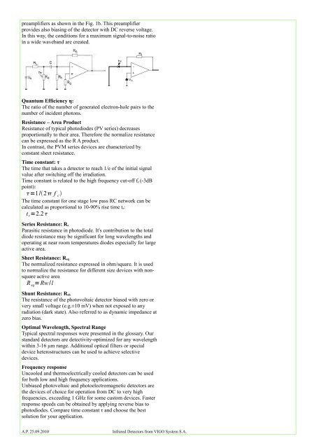
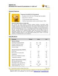
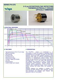
Shot Noise is due to the discrete nature of radiation, which iscomposed of photons arriving randomly in time. Absorbedphotons produce photoelectrons at random intervals, and thisvariation in current appears as a noise.Flicker or 1/f Noise is a frequency dependent noise that is stillnot fully understood. It occurs in any biased device. Its poweris proportional to 1/ f b where b is approx. 1. Forphotoconductors usually the 1/f knee is in the 1-20 kHz range.For biased LW<strong>IR</strong> photovoltaic detectors 1/f knee is in the 1-10MHz range.Noise Current and Noise Voltage: I n ,V nRoot mean square noise current or voltage.I n =I 2 n t V n =U 2 n tNoise Current and Noise Voltage Density:I ni n= f n= V n fi n , v nNoise Equivalent Power: NEPThe radiant power that produces signal to noise ratio of unity atthe output of the detector per square root bandwidth:NEP= nR v= i nR iinWHzNormalized Detectivity: D*The signal-to-noise ratio (SNR) at a detector output normalizedto 1 W radiant power, a 1 cm 2 detector optical area and a 1 Hzbandwidth. The higher the D* value, the better the detector.D *= R ii nA= R vv nA in cmHz1/2 /WThe D* is related to the NEP: D* = A 1/2 / NEP.The detectivity is the best parameter to characterize detectorsensitivity. The higher the D* the better the detector. The higherperformance can be achieved with optical immersion (Seriesnames with “I”) and thermoelectrical cooling (-2TE, -3TE and-4TE series).Operating Temperature: TBoth room temperature and TE cooled devices are offered. TEcooled devices give better performance but it is also morebulky and need appropriate handling. For more details on TEcooling see the chapter on TE Cooling and Cooler Controllers.Optical Area: AIt is an area where the incident radiant power is collected. Forrectangular photoconductive devices it is a contact width-length product where length is a distance between contacts.Spectral ResponseIt is often understood as a spectral responsivity or a spectraldetectivity. In detector data sheet it is presented as the D*(λ). Itcan be characterized by cut-on, cut-off wavelength, optimumwavelength, and peak wavelength.Optimum Wavelength: λ opThe wavelength for which a device was optimized for. For near<strong>IR</strong> detectors λ op is close to λ peak . In contrast, for uncooled longwavelength detectors λ op can be even larger then λ co . Forexample the uncooled λ op =10.6 µm detector has λ peak =6 to 7µm.Peak Wavelength: λ peakλ peak is a wavelength where a specified device has a maximumresponse.Cut-on and Cut-off Wavelengths: λ con, λ coffλ coff and λ con are minimum and maximum wavelength at whicha detector response reach 50% of the peak value. Cut-on forPC and PVM series is limited by GaAs transmittance (approx.0.9 µm) for MW<strong>IR</strong> single junction photovoltaic detectors cutoffis approx. 2.5 µm and for LW<strong>IR</strong> single junctionphotovoltaic detectors cut-off is approx. 3.5 µm. Customdetectors can be manufactured with different cut-on.Photocurrent: I phThe current signal <strong>from</strong> a photovoltaic device when exposed toincident radiant power. It is described by photovoltaic currentequation:I ph = QA D e gwhere:η - quantum efficiency, Q - photon flux, A d - active area,e - electron load, g - photoelectric gainPhotoelectric Gain: gNumber of electrons passing contacts per one absorbedphoton. In photovoltaic devices g it is close to 1.Photoconductive Devices (PC)Photoconductive Devices (PC) are detectors based onthe photoconductive effect. Infrared radiation generates chargecarriers in the semiconductor active region decreasing itsresistance. The resistance change is sensed as a voltage changeby applying a constant current bias. The optimum bias currentis specified in the Final Test Report and depends on thedetector size, operating temperature and spectralcharacteristics.Photoelectromagnetic Devices (PEM)PEM detectors are photovoltaic devices based onthe photoelectromagnetic effect. It relies on a spatialseparation of optically generated electrons and holes in amagnetic field applied to the semiconductor by a permanentmagnet built in to the detector housing. PEM detectors do notrequire electrical bias and show no flicker (1/f) noise. Thedevices are typically used as fast uncooled detectors of longwavelength radiation.Photovoltaic Devices (PV or PVM)Photovoltaic devices (photodiodes) are semiconductorstructures with one (PV) or multiple (PVM) homo- orheterojunctions. Absorbed photons produce electron-holepairs, resulting in external photocurrent. Reverse bias voltagemay be applied to increase differential resistance, reduce theshot noise, improve high frequency performance and dynamicrange. Reverse bias may increase responsivity in somedevices. Unfortunately, at the expense of flicker (1/f) noise inmost cases. PV detectors are more vulnerable to electrostaticdischarges than photoconductors.Circuitry for Photoconductive <strong>Detectors</strong>A typical circuit for PC MCT detectors is shown in fig. 1a.The detectors are usually low impedance devices and requirelow input voltage noise preamplifiers. A constant bias currentis used in the detector requiring a low noise DC voltage supplyor battery with current-limiting resistor R L . Typically, ACcoupling is used to prevent saturation of the preamplifier bydetector bias.Circuitry for Photovoltaic <strong>Detectors</strong>Transimpedance preamps that provide constant voltage reversebias are required for the best linearity and frequency responseextend high frequency response beyond the unbiased valuespublished in individual VIGO detector data sheets. Consult usfor options. This can be achieved using transimpedanceA.P. 25.09.2010Infrared <strong>Detectors</strong> <strong>from</strong> VIGO <strong>System</strong> S.A.
preamplifiers as shown in the Fig. 1b. This preamplifierprovides also biasing of the detector with DC reverse voltage.In this way, the conditions for a maximum signal-to-noise ratioin a wide waveband are created.R fhν-+V bQuantum Efficiency η:The ratio of the number of generated electron-hole pairs to thenumber of incident photons.Resistance – Area ProductResistance of typical photodiodes (PV series) decreasesproportionally to their area. Therefore the normalize resistancecan be expressed as the R A product.In contrast, the PVM series devices are characterized byconstant sheet resistance.Time constant: τThe time that takes a detector to reach 1/e of the initial signalvalue after switching off the irradiation.Time constant is related to the high frequency cut-off f c (-3dBpoint):=1/2 f c The time constant for one stage low pass RC network can becalculated as proportional to 10-90% rise time t r :t r =2.2Series Resistance: R sParasitic resistance in photodiode. It's contribution to the totaldiode resistance may be significant for long wavelengths andoperating at near room temperatures diodes especially for largeactive area.Sheet Resistance: R sqThe normalized resistance expressed in ohm/square. It is usedto normalize the resistance for different size devices with nonsquareactive areaR sq =Rw/lShunt Resistance: R shThe resistance of the photovoltaic detector biased with zero orvery small voltage (e.g.±10 mV) when not exposed to anyradiation (dark state). Also referred to as dynamic impedance atzero bias.Optimal Wavelength, Spectral RangeTypical spectral responses were presented in the glossary. Ourstandard detectors are detectivity-optimized for any wavelengthwithin 3-16 µm range. Additional optical filters or specialdevice heterostructures can be used to achieve selectivedevices.Frequency responseUncooled and thermoelectrically cooled detectors can be usedfor both low and high frequency applications.Unbiased photovoltaic and photoelectromagnetic detectors arethe devices of choice for operation <strong>from</strong> DC to very highfrequencies, exceeding 1 GHz for some custom devices. Fasterresponse speeds can be obtained by applying reverse bias tophotodiodes. Compare time constant τ and choose the bestsolution for your application.A.P. 25.09.2010Infrared <strong>Detectors</strong> <strong>from</strong> VIGO <strong>System</strong> S.A.