Indy R1000 Datasheet - Impinj
Indy R1000 Datasheet - Impinj
Indy R1000 Datasheet - Impinj

You also want an ePaper? Increase the reach of your titles
YUMPU automatically turns print PDFs into web optimized ePapers that Google loves.
<strong>Indy</strong><br />
Electrical, Mechanical, & Thermal Specification<br />
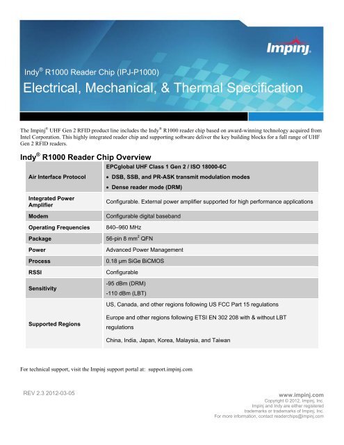
® <strong>R1000</strong> Reader Chip (IPJ-P1000)<br />
The <strong>Impinj</strong> ® UHF Gen 2 RFID product line includes the <strong>Indy</strong> ® <strong>R1000</strong> reader chip based on award-winning technology acquired from<br />
Intel Corporation. This highly integrated reader chip and supporting software deliver the key building blocks for a full range of UHF<br />
Gen 2 RFID readers.<br />
<strong>Indy</strong> ® <strong>R1000</strong> Reader Chip Overview<br />
Air Interface Protocol<br />
Integrated Power<br />
Amplifier<br />
REV 2.3 2012-03-05<br />
EPCglobal UHF Class 1 Gen 2 / ISO 18000-6C<br />
• DSB, SSB, and PR-ASK transmit modulation modes<br />
• Dense reader mode (DRM)<br />
Modem Configurable digital baseband<br />
Operating Frequencies 840–960 MHz<br />
Package 56-pin 8 mm 2 QFN<br />
Power Advanced Power Management<br />
Process 0.18 µm SiGe BiCMOS<br />
RSSI Configurable<br />
Sensitivity<br />
Supported Regions<br />
Configurable. External power amplifier supported for high performance applications<br />
-95 dBm (DRM)<br />
-110 dBm (LBT)<br />
US, Canada, and other regions following US FCC Part 15 regulations<br />
Europe and other regions following ETSI EN 302 208 with & without LBT<br />
regulations<br />
China, India, Japan, Korea, Malaysia, and Taiwan<br />
For technical support, visit the <strong>Impinj</strong> support portal at: support.impinj.com<br />
www.impinj.com<br />
Copyright © 2012, <strong>Impinj</strong>, Inc.<br />
<strong>Impinj</strong> and <strong>Indy</strong> are either registered<br />
trademarks or trademarks of <strong>Impinj</strong>, Inc.<br />
For more information, contact readerchips@impinj.com
<strong>Indy</strong> <strong>R1000</strong> ® Electrical, Mechanical, & Thermal Specification<br />
TABLE OF CONTENTS<br />
1 INTRODUCTION ............................................................................................................................................................................ 1<br />
1.1 TERMINOLOGY ............................................................................................................................................................................. 1<br />
1.2 REFERENCE DOCUMENTS ............................................................................................................................................................. 3<br />
2 ABOUT THIS DOCUMENT ........................................................................................................................................................... 4<br />
2.1 INDY <strong>R1000</strong> READER CHIP DIAGRAMS ......................................................................................................................................... 4<br />
3 PIN LISTING/SIGNAL DEFINITIONS ........................................................................................................................................ 6<br />
4 ELECTRICAL SPECIFICATIONS ............................................................................................................................................... 8<br />
4.1 ABSOLUTE MAXIMUM RATINGS ................................................................................................................................................... 8<br />
4.2 OPERATING CONDITIONS .............................................................................................................................................................. 9<br />
4.3 TRANSCEIVER FUNCTIONAL SPECIFICATIONS ............................................................................................................................... 9<br />
5 FUNCTIONAL DESCRIPTION ................................................................................................................................................... 14<br />
5.1 ANALOG RECEIVER DATA PATH ................................................................................................................................................. 15<br />
5.1.1 Receiver Front-end Circuitry ............................................................................................................................................. 15<br />
5.1.2 LO Input ............................................................................................................................................................................. 16<br />
5.1.3 Receive RF Interface .......................................................................................................................................................... 16<br />
5.1.4 Receive Baseband Interface ............................................................................................................................................... 16<br />
5.2 DIGITAL RECEIVER DATA PATH ................................................................................................................................................. 17<br />
5.2.1 Decimation Filters and AGC Control ................................................................................................................................ 17<br />
5.2.2 Digital Channel Filter ........................................................................................................................................................ 18<br />
5.2.3 RSSI .................................................................................................................................................................................... 18<br />
5.3 DIGITAL TRANSMITTER DATA PATH .......................................................................................................................................... 18<br />
5.3.1 Baseband Encoding and Pulse Shaping ............................................................................................................................. 19<br />
5.3.2 Power Scaling .................................................................................................................................................................... 20<br />
5.3.3 Hilbert Transformer ........................................................................................................................................................... 20<br />
5.3.4 Frequency Shifter ............................................................................................................................................................... 20<br />
5.3.5 AM Pre-distortion............................................................................................................................................................... 20<br />
5.3.6 Upsampling ........................................................................................................................................................................ 20<br />
5.3.7 Sigma Delta Digital to Analog Converter .......................................................................................................................... 20<br />
5.4 ANTENNA CONFIGURATION SCENARIOS ..................................................................................................................................... 22<br />
5.5 RF POWER DETECTION ............................................................................................................................................................... 23<br />
5.6 TRANSMITTER MODES ................................................................................................................................................................ 23<br />
5.6.1 Full Power Non-linear Mode (DSB-ASK) .......................................................................................................................... 23<br />
5.6.2 Low Power Non-linear Mode (DSB-ASK) .......................................................................................................................... 24<br />
5.6.3 Linear Mode ....................................................................................................................................................................... 24<br />
6 DEVICE CONTROL AND PROGRAMMING ........................................................................................................................... 25<br />
6.1 SERIAL INTERFACE ..................................................................................................................................................................... 26<br />
6.1.1 Parallel Interface ............................................................................................................................................................... 28<br />
ii Revision 2.3, Copyright © 2012, <strong>Impinj</strong>, Inc.
<strong>Indy</strong> <strong>R1000</strong> ® Electrical, Mechanical, & Thermal Specification<br />
6.2 REGISTER MAP ........................................................................................................................................................................... 30<br />
7 PERFORMANCE CHARACTERISTICS - PRELIMINARY ................................................................................................... 56<br />
7.1 RECEIVER COMPRESSION POINT ................................................................................................................................................. 56<br />
7.2 RF TO IF CONVERSION GAIN AND GAIN FLATNESS .................................................................................................................... 57<br />
7.3 CARRIER SETTLING TIME ........................................................................................................................................................... 57<br />
7.4 RX SENSITIVITY TESTING ........................................................................................................................................................... 58<br />
7.5 TRANSMIT OUTPUT SPECTRAL TESTING ..................................................................................................................................... 64<br />
7.6 GAIN CONTROL RESOLUTION AND DYNAMIC RANGE ................................................................................................................. 68<br />
7.7 ADC TESTING ............................................................................................................................................................................ 70<br />
7.8 AUX. DAC TESTING ................................................................................................................................................................... 70<br />
8 PACKAGE INFORMATION ........................................................................................................................................................ 73<br />
8.1 PACKAGE INFORMATION ............................................................................................................................................................ 73<br />
8.2 PACKAGE MARKINGS ................................................................................................................................................................. 76<br />
NOTICES: ............................................................................................................................................................................................... 77<br />
FIGURES<br />
FIGURE 1: INDY <strong>R1000</strong> READER CHIP TOP LEVEL RF BLOCK DIAGRAM .................................................................................................... 4<br />
FIGURE 2: INDY <strong>R1000</strong> READER CHIP TOP LEVEL DIGITAL BLOCK DIAGRAM ........................................................................................... 4<br />
FIGURE 3: INDY <strong>R1000</strong> READER CHIP SAMPLE APPLICATION ..................................................................................................................... 5<br />
FIGURE 4: ANALOG RECEIVER DATA PATH .............................................................................................................................................. 15<br />
FIGURE 5: RECEIVER FRONT-END EXTERNAL INTERFACES ....................................................................................................................... 15<br />
FIGURE 6: LO INPUT EXTERNAL INTERFACES ........................................................................................................................................... 16<br />
FIGURE 7: OVERVIEW OF THE DIGITAL PART OF THE TRANSMITTER DATA PATH ..................................................................................... 19<br />
FIGURE 8: PRINCIPLE OF SIGMA-DELTA DAC ........................................................................................................................................... 21<br />
FIGURE 9: SINGLE ANTENNA SCENARIO ................................................................................................................................................... 22<br />
FIGURE 10: DUAL ANTENNA SCENARIO .................................................................................................................................................... 22<br />
FIGURE 11: INDY <strong>R1000</strong> READER CHIP TRANSMIT WITH EXTERNAL PA (DSB ASK OR PR-ASK) .......................................................... 24<br />
FIGURE 12: SERIAL INTERFACE FRAME FORMAT ...................................................................................................................................... 26<br />
FIGURE 13: SERIAL INTERFACE T2R TIMING ............................................................................................................................................ 26<br />
FIGURE 14: SERIAL INTERFACE R2T TIMING ............................................................................................................................................ 27<br />
FIGURE 15: PARALLEL INTERFACE READ TIMING ..................................................................................................................................... 28<br />
FIGURE 16: PARALLEL INTERFACE WRITE TIMING ................................................................................................................................... 28<br />
FIGURE 17: CARRIER SETTLING TIME ....................................................................................................................................................... 57<br />
FIGURE 18: PACKET ERROR RATE TEST SETUP - MONOSTATIC CONFIGURATION ..................................................................................... 58<br />
FIGURE 19: PACKET ERROR RATE TEST SETUP - BI-STATIC CONFIGURATION .......................................................................................... 59<br />
FIGURE 20: PACKET ERROR RATE TEST SETUP - REAL TAG ..................................................................................................................... 59<br />
FIGURE 21: RX SENSITIVITY PLOT: FM0, 40 KBPS, NO SELF JAMMER ..................................................................................................... 60<br />
FIGURE 22: RX SENSITIVITY PLOT: FM0, 40 KBPS, MEDIUM IFLNA GAIN SETTING ............................................................................... 61<br />
FIGURE 23: RX SENSITIVITY PLOT: FM0, 40 KBPS, +2 DBM, SELF JAMMER ............................................................................................ 62<br />
FIGURE 24: RX SENSITIVITY PLOT: FM0, 40 KBPS, LOW RF GAIN, NO SELF JAMMER ............................................................................. 62<br />
FIGURE 25: M4 62.5K (DENSE READER MODE) ....................................................................................................................................... 63<br />
FIGURE 26: M4 62.5K FAR AWAY INTERFERER ........................................................................................................................................ 63<br />
FIGURE 27: INDY <strong>R1000</strong> READER CHIP TRANSMIT MODULATION AND MASK FOR DSB, TARI=25 SEC, X=0.5 ..................................... 64<br />
FIGURE 28: INDY <strong>R1000</strong> READER CHIP TRANSMIT MODULATION AND MASK FOR DSB, TARI=25 µSEC, X=1 ......................................... 64<br />
FIGURE 29: INDY <strong>R1000</strong> READER CHIP TRANSMIT MODULATION AND MASK FOR PR-ASK, TARI=12.5 µSEC, X=0.5 ............................ 65<br />
FIGURE 30: INDY <strong>R1000</strong> READER CHIP TRANSMIT MODULATION AND MASK FOR PR-ASK, TARI=12.5 µSEC, X=1 ............................... 66<br />
FIGURE 31: INDY <strong>R1000</strong> READER CHIP TRANSMIT MODULATION AND MASK FOR PR-ASK, TARI=25 µSEC, X=0.5 ............................... 66<br />
FIGURE 32: INDY <strong>R1000</strong> READER CHIP TRANSMIT MODULATION AND MASK FOR PR-ASK, TARO= 25 µSEC, X=1 ................................ 66<br />
FIGURE 33: INDY <strong>R1000</strong> READER CHIP TRANSMIT MODULATION AND MASK FOR SSB, TARI=12.5 µSEC, X=0.5 ................................... 67<br />
FIGURE 34: INDY <strong>R1000</strong> READER CHIP TRANSMIT MODULATION AND MASK FOR SSB, TARI=12.5 µSEC, X=1 ...................................... 67<br />
Revision 2.3, Copyright © 2012, <strong>Impinj</strong>, Inc. iii
<strong>Indy</strong> <strong>R1000</strong> ® Electrical, Mechanical, & Thermal Specification<br />
FIGURE 35: INDY <strong>R1000</strong> READER CHIP TRANSMIT MODULATION AND MASK FOR SSB, TARI=25 µSEC, X=0.5 ...................................... 67<br />
FIGURE 36: INDY <strong>R1000</strong> READER CHIP TRANSMIT MODULATION AND MASK FOR SSB, TARI=25 µSEC, X=1 ......................................... 68<br />
FIGURE 37: TX OUTPUT POWER SCALER GAIN CONTROL ......................................................................................................................... 69<br />
FIGURE 38: ADC DYNAMIC RANGE AND LINEARITY ................................................................................................................................ 70<br />
FIGURE 39: DAC LINEARITY AND RANGE ................................................................................................................................................ 71<br />
FIGURE 40: INTEGRAL NON-LINEARITY OF PA BIAS AND PA REGULATOR DACS ................................................................................... 71<br />
FIGURE 41: DIFFERENTIAL NON-LINEARITY OF PA BIAS AND PA REGULATOR DACS ............................................................................. 72<br />
FIGURE 42: INDY <strong>R1000</strong> READER CHIP PACKAGE TOP VIEW ................................................................................................................... 73<br />
FIGURE 43: INDY <strong>R1000</strong> READER CHIP PACKAGE TOP VIEW ................................................................................................................... 74<br />
FIGURE 44: INDY <strong>R1000</strong> READER CHIP PACKAGE BOTTOM AND SIDE VIEWS .......................................................................................... 75<br />
TABLES<br />
TABLE 1: TERMINOLOGY ............................................................................................................................................................................ 1<br />
TABLE 2: PROTOCOL SPECIFICATION DOCUMENTS ..................................................................................................................................... 3<br />
TABLE 3: LOCAL REGULATION DOCUMENTS .............................................................................................................................................. 3<br />
TABLE 4: PIN LISTING AND SIGNAL DEFINITIONS ....................................................................................................................................... 6<br />
TABLE 5: ABSOLUTE MAXIMUM RATINGS .................................................................................................................................................. 8<br />
TABLE 6: OPERATING CONDITIONS ............................................................................................................................................................ 9<br />
TABLE 7A: POWER CONSUMPTION SPECIFICATIONS IN MISSION MODE (READING TAGS) AND RESET ........................................................ 9<br />
TABLE 8: INDY <strong>R1000</strong> READER CHIP - RECEIVER SPECIFICATIONS .......................................................................................................... 10<br />
TABLE 9: INDY <strong>R1000</strong> READER CHIP - TRANSMITTER SPECIFICATIONS .................................................................................................... 11<br />
TABLE 10: INDY <strong>R1000</strong> READER CHIP EXTERNAL LO INPUT ................................................................................................................... 11<br />
TABLE 11: INDY <strong>R1000</strong> READER CHIP ENVELOPE DETECTORS ................................................................................................................ 11<br />
TABLE 12: INDY <strong>R1000</strong> READER CHIP SYNTHESIZER ............................................................................................................................... 12<br />
TABLE 13: INDY <strong>R1000</strong> READER CHIP CLOCK OUTPUT, DACS, AND ADCS ............................................................................................ 13<br />
TABLE 14: INDY <strong>R1000</strong> READER CHIP DIGITAL INTERFACE ..................................................................................................................... 13<br />
TABLE 15: SPECIFICATION OF BASEBAND ENCODING AND PULSE SHAPING BLOCK ................................................................................. 19<br />
TABLE 16: SPECIFICATION OF SIGMA-DELTA DAC ................................................................................................................................... 21<br />
TABLE 17: STRAPPING OPTIONS ............................................................................................................................................................... 25<br />
TABLE 18: PIN FUNCTIONALITY PER MODEV ........................................................................................................................................... 25<br />
TABLE 19: SERIAL INTERFACE TIMING REQUIREMENTS ........................................................................................................................... 27<br />
TABLE 20: PARALLEL INTERFACE TIMING CONDITIONS ........................................................................................................................... 29<br />
TABLE 21: DIRECT REGISTER MAP, B REVISION ....................................................................................................................................... 30<br />
TABLE 22: INDIRECT REGISTER MAP, B0 STEPPING .................................................................................................................................. 31<br />
TABLE 23: RECEIVER COMPRESSION POINT .............................................................................................................................................. 56<br />
TABLE 24: GAIN AT 100 KHZ IF (DB) ...................................................................................................................................................... 57<br />
TABLE 25: MIXER GAIN SETTINGS............................................................................................................................................................ 69<br />
TABLE 26: PA POWER GAIN SETTINGS ..................................................................................................................................................... 69<br />
iv Revision 2.3, Copyright © 2012, <strong>Impinj</strong>, Inc.
1 Introduction<br />
<strong>Indy</strong> <strong>R1000</strong> ® Electrical, Mechanical, & Thermal Specification<br />
<strong>Impinj</strong> ® ’s <strong>Indy</strong> ® <strong>R1000</strong> reader chip is a highly integrated, high-performance, low power, SiGe BiCMOS device for ISO18000-6C and Electronic<br />
Product Council (EPC) Gen 2 applications. The <strong>Indy</strong> <strong>R1000</strong> reader chip supports a zero intermediate frequency (ZIF) architecture in the worldwide<br />
UHF industrial, science, and medical (ISM) band. The <strong>Indy</strong> <strong>R1000</strong> reader chip comprises all of the RF blocks to interrogate and receive data from<br />
compatible RFID tags, specifically:<br />
• High compression point quadrature downconverting mixer<br />
• Fully integrated voltage controlled oscillator (VCO)<br />
• Variable receiver (RX) gain control<br />
• Integrated Power Amplifier (PA)<br />
• Integrated RF envelope detectors for forward and reverse power sense<br />
• Integrated multipurpose Analog-to-Digital Converts (ADCs) and Digital-to-Analog Converters (DACs)<br />
• Configurable digital baseband<br />
• High speed synchronous serial bus or 4-bit parallel bus control<br />
When used in the <strong>Indy</strong> <strong>R1000</strong> Development Platform, which includes an example protocol processor and radio control implementation, the result is a<br />
fully functional UHF RFID reader.<br />
1.1 Terminology<br />
Term Description<br />
Table 1: Terminology<br />
ADC Analog-to-Digital Converter<br />
AGC Automatic Gain Control<br />
AM Amplitude Modulation<br />
ASK Amplitude Shift Keying<br />
AUX Auxiliary<br />
BPF Bandpass Filter<br />
Class 0<br />
Tags and readers conforming to MIT Auto-ID Center,<br />
Class 0 RFID Tag Protocol Specification<br />
CORDIC COordinate Rotation DIgital Computer<br />
CW Continuous Wave<br />
DAC Digital-to-Analog Converter<br />
DFT Discrete Fourier Transform<br />
DSB Double Sideband<br />
EOT End of Transfer<br />
EPC Electronic Product Council<br />
Revision 2.3, Copyright © 2012, <strong>Impinj</strong>, Inc. 1
<strong>Indy</strong> <strong>R1000</strong> ® Electrical, Mechanical, & Thermal Specification<br />
Term Description<br />
FCC Federal Communications Commission (US Regulatory Body)<br />
FIFO First In, First Out<br />
FIR Finite Impulse Response<br />
I In-phase<br />
IF Intermediate Frequency<br />
IIR Infinite Impulse Response<br />
I-Q In-phase Quadrature<br />
ISM Industrial, Science, and Medical<br />
ISO International Standards Organization<br />
ISO18000 Tags and readers conforming to ISO/IEC FDIS 18000-6:2003(E)<br />
LBT Listen Before Talk<br />
LFSR Linear Feedback Shift Registers<br />
LNA Low Noise Amplifier<br />
LO Local Oscillator<br />
LUT Lookup Table<br />
MSB Most Significant Bit<br />
NCO Numerically Controlled Oscillator<br />
PA Power Amplifier<br />
PLL Phase Locked Loop<br />
PoE Power over Ethernet<br />
PR Phase Reversal<br />
Q Quadrature-phase<br />
RF Radio Frequency<br />
RFID Radio Frequency Identification<br />
RSSI Received Signal Strength Indicator<br />
RX Receiver<br />
SSB Single Sideband<br />
TBD To Be Determined<br />
TX Transmitter<br />
TCXO Temperature Compensated Crystal Oscillator<br />
UHF Ultra High Frequency<br />
VCO Voltage Controlled Oscillator<br />
2 Revision 2.3, Copyright © 2012, <strong>Impinj</strong>, Inc.
1.2 Reference Documents<br />
<strong>Indy</strong> <strong>R1000</strong> ® Electrical, Mechanical, & Thermal Specification<br />
The <strong>Indy</strong> <strong>R1000</strong> reader chip is fully compliant with the protocol specifications provided in Table 2, as well as with the local regulations in Table 3.<br />
Table 2: Protocol Specification Documents<br />
Document Document Number<br />
ISO/IEC FDIS 18000-6:2005 Version 2.0, August 2004<br />
Table 3: Local Regulation Documents<br />
Document Document Number<br />
FCC 47 CFR Ch. 1, part 15 10-1-98 Edition<br />
ETSI EN 302 208-1 V1.1.1<br />
Revision 2.3, Copyright © 2012, <strong>Impinj</strong>, Inc. 3
<strong>Indy</strong> <strong>R1000</strong> ® Electrical, Mechanical, & Thermal Specification<br />
2 About this Document<br />
This document constitutes the electrical, mechanical, and thermal specifications for the <strong>Indy</strong> <strong>R1000</strong> reader chip. It contains a functional overview,<br />
mechanical data, package signal locations, and targeted electrical specifications.<br />
2.1 <strong>Indy</strong> <strong>R1000</strong> Reader Chip Diagrams<br />
A top level block diagram of the analog parts of the <strong>Indy</strong> <strong>R1000</strong> reader chip is shown in Figure 1. The architecture is based on direct conversion for<br />
both the transmitter and receiver. A block diagram for the digital parts is shown in Figure 2, and a sample application for the <strong>Indy</strong> <strong>R1000</strong> reader chip<br />
is illustrated in Figure 3.<br />
Figure 1: <strong>Indy</strong> <strong>R1000</strong> Reader Chip Top Level RF Block Diagram<br />
Figure 2: <strong>Indy</strong> <strong>R1000</strong> Reader Chip Top Level Digital Block Diagram<br />
4 Revision 2.3, Copyright © 2012, <strong>Impinj</strong>, Inc.
<strong>Indy</strong> <strong>R1000</strong> ® Electrical, Mechanical, & Thermal Specification<br />
Figure 3: <strong>Indy</strong> <strong>R1000</strong> Reader Chip Sample Application<br />
Revision 2.3, Copyright © 2012, <strong>Impinj</strong>, Inc. 5
<strong>Indy</strong> <strong>R1000</strong> ® Electrical, Mechanical, & Thermal Specification<br />
3 Pin Listing/Signal Definitions<br />
Table 4: Pin Listing and Signal Definitions<br />
Pin # Pin Name Type + Description<br />
1 Vdd_rx_rf 5.0 V Supply for receive RF<br />
2<br />
3<br />
4<br />
5<br />
6<br />
7<br />
8<br />
9<br />
10<br />
11<br />
RX_p<br />
RX_n<br />
Atest0<br />
Atest1<br />
LO_p<br />
LO_n<br />
Atest2<br />
Atest3<br />
Detector_p<br />
Detector_n<br />
RF In Differential receive RF input<br />
A Analog test bus<br />
RF In Differential RF input from a high impedance tap on transmit path<br />
A Analog test bus<br />
RF In Differential peak detector input<br />
12 Temp A In Voltage input from a temperature sensor (General Purpose ADC)<br />
13 Vdd_tx_rf 3.3 V Supply for transmit RF, except for PA<br />
14 Vdd_tx_pre 1.8 V PA pre-driver supply<br />
15 Vdd_tx_pa 1.8 V PA supply<br />
16 Reserved Reserved for Future Use<br />
17<br />
18<br />
PA_p<br />
PA_n<br />
RF Out Differential TX output for all modes<br />
19 Vdd_tx_ana 3.3 V Supply for transmit analog<br />
20<br />
21<br />
22<br />
23<br />
PA_modp<br />
PA_modn<br />
Ant_sense0<br />
Ant_sense1<br />
A Out Differential output voltage of PA modulator DAC to apply AM to the PA<br />
A In General Purpose ADCs<br />
24 PA_reg A Out General Purpose 8-bit DAC. Can be used to control external PA regulators.<br />
25 PA_bias A Out General Purpose 8-bit DAC. Can be used to control external PA bias.<br />
26 D In Manufacturing Test Pin<br />
27 Chip_resetn D In<br />
28 Vdd_dig 1.8 V Digital supply<br />
29 Vdd_io 3.3 V I/O supplies<br />
30<br />
31<br />
32<br />
33<br />
DA0/T2R_DAT[0]<br />
DA1/T2R_DAT[1]<br />
DA2/T2R_DAT[2]<br />
DA3/T2R_FRM<br />
D Bi<br />
(slew rate<br />
limited)<br />
Bidirectional data interface, multiplexed with SSP T2R frame and data signals, Power-up state: HiZ<br />
34 ALE / R2T_FRM D Bi Address Latch Enable input, multiplexed with SSP R2T frame output<br />
35 CSn / R2T_CLK D In Active-low chip select active low, multiplexed with SSP R2T clock<br />
6 Revision 2.3, Copyright © 2012, <strong>Impinj</strong>, Inc.
Pin # Pin Name Type + Description<br />
<strong>Indy</strong> <strong>R1000</strong> ® Electrical, Mechanical, & Thermal Specification<br />
36 RDn / T2R_CLK D Bi Read strobe, active low, multiplexed with SSP T2R clock signal<br />
37 WRn / R2T_D[0] D In Write strobe, active low, multiplexed with SSP R2T data signal<br />
38 IRQn D Bi Interrupt, active low, Power-up state: HiZ<br />
39<br />
40<br />
Dtest0<br />
Dtest1<br />
D Bi<br />
At the termination of reset, Dtest1 is sensed and is used to configure the digital pins for parallel or<br />
serial operation.<br />
Additionally, DTEST0 must be held low as the <strong>R1000</strong> is coming out of reset to disable factory test<br />
mode behavior.<br />
41 CLK_out D Bi Reference clock output for other chips<br />
42 TCXO Clk In Reference clock input from a 24 MHz AC coupled TCXO<br />
43 Vdd_clkref 1.8 V Supply of clock reference input buffer<br />
44 Vdd_pll 3.3 V PLL Supply<br />
45<br />
46<br />
PLL_fil0<br />
PLL_fil1<br />
A Nodes for external PLL filter<br />
47 Vdd_vco 3.3 V VCO supply<br />
48<br />
49<br />
50<br />
51<br />
52<br />
53<br />
54<br />
55<br />
Amp_Qp<br />
Amp_Qn<br />
Mix_Qn<br />
Mix_Qp<br />
Amp_Ip<br />
Amp_In<br />
Mix_In<br />
Mix_Ip<br />
A In Q post-mixer amplifier input<br />
A Out Q Mixer output<br />
A In I post-mixer amplifier input<br />
A Out I Mixer output<br />
56 Vdd_rx_ana 3.3 V RX analog supply<br />
Paddle GND GND Single Chip Ground<br />
+ In the Type column, A denotes analog, while D denotes digital.<br />
Revision 2.3, Copyright © 2012, <strong>Impinj</strong>, Inc. 7
<strong>Indy</strong> <strong>R1000</strong> ® Electrical, Mechanical, & Thermal Specification<br />
4 Electrical Specifications<br />
4.1 Absolute Maximum Ratings<br />
The absolute maximum ratings (see Table 5) define limitations for electrical and thermal stresses. These limits prevent permanent damage to the<br />
<strong>Indy</strong> <strong>R1000</strong> reader chip.<br />
aution: Operation outside these maximum ratings might result in permanent damage to the device.<br />
Table 5: Absolute Maximum Ratings<br />
Parameter Min Max Unit Conditions<br />
Digital core supply voltage<br />
Digital I/O supply voltage<br />
Analog PA supply voltage<br />
Analog clock ref supply voltage<br />
Analog supply voltage<br />
Analog VCO supply voltage<br />
Analog RF RX supply voltage<br />
Maximum voltage on nonsupply<br />
pins<br />
-0.5 2.1 V Vdd_dig<br />
-0.5 3.6 V Vdd_io<br />
-0.5 2.1 V Vdd_tx_pa/Vdd_tx_pre<br />
-0.5 2.1 V Vdd_clkref<br />
-0.5 3.6 V<br />
Vdd_pll, Vdd_rx_ana, Vdd_tx_ana,<br />
Vdd_tx_rf<br />
-0.5 3.6 V Vdd_vco<br />
-0.5 5.5 V Vdd_rx_rf<br />
-0.5<br />
-1.0<br />
RF input power -<br />
3.6<br />
3.6<br />
+15<br />
8:1<br />
Storage temperature -45 +110<br />
8 Revision 2.3, Copyright © 2012, <strong>Impinj</strong>, Inc.<br />
V<br />
V<br />
dBm<br />
VSWR<br />
o C<br />
Outputs<br />
Inputs<br />
PA_out<br />
Rx, Detector, LO
4.2 Operating Conditions<br />
<strong>Indy</strong> <strong>R1000</strong> ® Electrical, Mechanical, & Thermal Specification<br />
This section shows operating voltage, frequency, and temperature specifications for the <strong>Indy</strong> <strong>R1000</strong> reader chip. Table 6 provides the supported<br />
operating conditions:<br />
Table 6: Operating Conditions<br />
Parameter Min Typ Max Unit Conditions<br />
Digital core supply voltage 1.7 1.8 1.9 V Vdd_dig<br />
Digital I/O supply voltage 3.135 3.3 3.465 V Vdd_io<br />
Analog PA supply voltage 1.7 1.8 1.9 V Vdd_tx_pa/Vdd_tx_pre<br />
Analog clock ref supply voltage 1.7 1.8 1.9 V Vdd_clkref<br />
Analog supply voltage 3.135 3.3 3.465 V<br />
Vdd_pll, Vdd_rx_ana, Vdd_tx_ana,<br />
Vdd_tx_rf<br />
Analog VCO supply voltage 3.135 3.3 3.465 V Vdd_vco<br />
Analog RF RX supply voltage 4.75 5.0 5.25 V Vdd_rx_rf<br />
Analog supply ripple - - TBD mVp<br />
For all supply rails<br />
Frequency of ripple TBD MHz<br />
Digital supply ripple - - TBD mVp Frequency of ripple TBD MHz<br />
Operating temperature -20 - +85<br />
4.3 Transceiver Functional Specifications<br />
o C Case Temperature<br />
Table 7a: Power Consumption Specifications in Mission Mode (Reading Tags) and Reset<br />
Parameter Min Typ Max Unit Conditions<br />
Power consumption 1250 mW @ 17dBm<br />
Power consumption 1000 mW @ 12dBm<br />
Power consumption 950 mW @ 6.1dBm<br />
Power consumption measurements were taken from and based on the <strong>Indy</strong> <strong>R1000</strong> Development Platform which should be representative of a real<br />
world application. Note: this data is based on a front end mixer power supply of 3.3V. Using a 5V rail for the front end mixer increases the P1dB of<br />
the mixer and increases power consumption by 200mW in high gain mode and 100 mW in low gain mode.<br />
Table 7b: <strong>Indy</strong> <strong>R1000</strong> Reader Chip - Receiver Specifications<br />
Power Rail<br />
Voltage<br />
Typical after<br />
Reset Current<br />
(mA)<br />
Tag Read Current<br />
(mA)<br />
Voltage Notes<br />
P1.8V_RF 6 205 1.8V analog<br />
P3.3V_RF 195 226 3.3V analog<br />
P5V_RF 17 17 5V analog<br />
Revision 2.3, Copyright © 2012, <strong>Impinj</strong>, Inc. 9
<strong>Indy</strong> <strong>R1000</strong> ® Electrical, Mechanical, & Thermal Specification<br />
Table 8 shows nominal design values for <strong>R1000</strong> power supply consumption.<br />
Table 8: <strong>Indy</strong> <strong>R1000</strong> Reader Chip - Receiver Specifications<br />
Parameter Min Typ Max Unit Conditions<br />
Input frequency 840 960 MHz<br />
Differential input impedance 50 Ω<br />
Frequency = 900 MHz<br />
Note Recommended Balun in App<br />
Note<br />
Differential input match 9 dB S11<br />
Signal voltage gain<br />
Noise figure with jammer<br />
Noise figure without jammer<br />
Power level<br />
4<br />
13<br />
TBD<br />
TBD<br />
11<br />
14<br />
10 Revision 2.3, Copyright © 2012, <strong>Impinj</strong>, Inc.<br />
dB<br />
dB<br />
dB<br />
dB<br />
dB<br />
dB<br />
IIP2 +50 dBm<br />
Low gain path<br />
High gain path<br />
LNA, mixer and LO<br />
Low gain path<br />
High gain path<br />
LBT high gain path<br />
LBT low gain path<br />
I and Q phase error TBD deg At IF output<br />
I and Q amplitude error TBD dB At IF output<br />
LO leakage -60 dB At RF input<br />
IF bandwidth 10 MHz<br />
Chip sensitivity level (1% PER)<br />
In-channel RSSI dynamic<br />
range in low gain<br />
In-channel RSSI dynamic<br />
range in high gain<br />
TBD<br />
TBD<br />
-96.5<br />
-95<br />
-93.5<br />
-92<br />
-25<br />
-85<br />
-45<br />
-110<br />
TBD<br />
TBD<br />
dBm<br />
dBm<br />
dBm<br />
dBm<br />
dBm<br />
dBm<br />
dBm<br />
dBm<br />
RSSI register size 8 Bits<br />
Co-channel selectivity TBD<br />
Adjacent channel selectivity TBD<br />
Blocking and desensitization TBD TBD<br />
• FM0 40 kbps, IFLNA: High Gain,<br />
RF: High Gain, No Self-Jammer<br />
• Miller 4 62.5 kbps, IFLNA: High, RF:<br />
High, No Self-Jammer<br />
• FM0 40 kbps, IFLNA: High Gain,<br />
RF: Low Gain, No Self-Jammer<br />
• Miller 4 62.5 kbps, IFLNA: High<br />
Gain, RF: Low Gain, No Self-Jammer<br />
Maximum level<br />
Minimum level<br />
Maximum level<br />
Minimum level<br />
Dependent on external adjacent<br />
channel filter<br />
Dependent on external adjacent<br />
channel filter<br />
LO input power -20 0 dBm TBD
<strong>Indy</strong> <strong>R1000</strong> ® Electrical, Mechanical, & Thermal Specification<br />
Parameter Min Typ Max Unit Conditions<br />
LO input impedance 50 Ω Frequency = 900 MHz<br />
Table 9: <strong>Indy</strong> <strong>R1000</strong> Reader Chip - Transmitter Specifications<br />
Parameter Min. Typ. Max. Unit Conditions<br />
TX differential load impedance 50 Ω<br />
TX output power<br />
Linear mode OIP3<br />
TX output power temperature<br />
variation<br />
TX output power absolute<br />
tolerance<br />
TX output power range<br />
TX output power step size<br />
AM control signal to external<br />
PA<br />
+20<br />
+10<br />
Frequency = 900 MHz<br />
Output port of the Balun<br />
Revision 2.3, Copyright © 2012, <strong>Impinj</strong>, Inc. 11<br />
+17<br />
dBm<br />
dBm<br />
+27 dBm<br />
TBD dB<br />
Linear, P1dB<br />
Linear, Modulated<br />
CW with closed loop power control<br />
-20º to 75ºC<br />
TBD dB With closed loop power control<br />
15 dB Linear mode (Analog Resolution)<br />
2 dB Linear mode (Analog Range)<br />
0.7 Vp<br />
Table 10: <strong>Indy</strong> <strong>R1000</strong> Reader Chip External LO Input<br />
Parameter Min Typ Max Unit Conditions<br />
Input impedance 50 Ω<br />
Differential input match -9 dB S11<br />
Input frequency 840 960 MHz<br />
Input power level -20 0 dBm<br />
Supply voltage 3.3 V Vdd_tx_rf<br />
Table 11: <strong>Indy</strong> <strong>R1000</strong> Reader Chip Envelope Detectors<br />
Parameter Min Typ Max Unit Conditions<br />
Forward power detection TBD TBD dBm At LO input<br />
Reverse power detection TBD TBD<br />
Wideband listen before talk<br />
TBD<br />
TBD<br />
TBD<br />
TBD<br />
dBm<br />
dBm<br />
dBm<br />
dBm<br />
At detector input<br />
At RX input<br />
At RX input
<strong>Indy</strong> <strong>R1000</strong> ® Electrical, Mechanical, & Thermal Specification<br />
Table 12: <strong>Indy</strong> <strong>R1000</strong> Reader Chip Synthesizer<br />
Parameter Min Typ Max Unit Conditions<br />
Frequency Range 840 960 MHz<br />
Frequency Grid<br />
25<br />
100<br />
250<br />
12 Revision 2.3, Copyright © 2012, <strong>Impinj</strong>, Inc.<br />
kHz<br />
kHz<br />
kHz<br />
Europe (ETSI 300 220)<br />
Europe (ETSI 302 208)<br />
US (FCC)<br />
Reference Input Frequency 24 MHz TCXO Specification<br />
Reference Frequency<br />
Tolerance<br />
Reference Input Level 0.8 Vp<br />
Reference Duty Cycle 40 60 %<br />
PLL settling time within 1% of<br />
frequency step<br />
10 ppm TCXO Specification<br />
140 470 µs<br />
100 KHz grid, recommended PLL<br />
Loop filter configuration<br />
TX Phase Noise -116 dBc/Hz ∆f = 200 kHz<br />
Broadband Noise -144 dBc/Hz ∆f = 3.6MHz<br />
TX In-band spurious emissions -69 dBc RBW = 3 kHz, average detector<br />
TX Out-of-band spurious<br />
emissions measured with<br />
balun<br />
RX Spurious emissions<br />
54<br />
-42<br />
-57<br />
-47<br />
dBm<br />
dBm<br />
dBm<br />
dBm<br />
Below 1 GHz (ETSI)<br />
RBW = 120 kHz, peak detector<br />
Above 960 MHz (FCC)<br />
RBW = 1 MHz, average detector<br />
Measured with balun (and BPF)<br />
30 MHz to 1 GHz<br />
1 to 12.75 GHz
<strong>Indy</strong> <strong>R1000</strong> ® Electrical, Mechanical, & Thermal Specification<br />
Table 13: <strong>Indy</strong> <strong>R1000</strong> Reader Chip Clock Output, DACs, and ADCs<br />
Parameter Min Typ Max Unit Conditions<br />
Maximum load capacitance on<br />
CLK_out<br />
10<br />
10<br />
10<br />
10<br />
10<br />
Antenna input detection range 0.3 2.7 V<br />
Antenna input detection<br />
resolution<br />
Revision 2.3, Copyright © 2012, <strong>Impinj</strong>, Inc. 13<br />
pF<br />
pF<br />
pF<br />
pF<br />
pF<br />
8 bits<br />
Temperature sensor range 0.3 2.7 V<br />
Temperature sensor resolution 8 bits<br />
PA bias output range 0.3 2.7 V<br />
Output clock rate 48 MHz<br />
24 MHz<br />
12 MHz<br />
6 MHz<br />
3 MHz<br />
PA bias resolution 8 bits SD DAC implementation<br />
PA regulator ctrl output range 0.3 2.7 V<br />
PA regulator ctrl resolution 8 bits SD DAC implementation<br />
Table 14: <strong>Indy</strong> <strong>R1000</strong> Reader Chip Digital Interface<br />
Parameter Min Typ Max Units Conditions<br />
Input high voltage 1.5 Vdd V<br />
Input low voltage 0 0.9 V<br />
Output high voltage 2.3 Vdd V<br />
Output low voltage 0 0.7 V<br />
Input leakage current -10 10 µA<br />
Input pin capacitance 10 pF
<strong>Indy</strong> <strong>R1000</strong> ® Electrical, Mechanical, & Thermal Specification<br />
5 Functional Description<br />
The transmitter supports both in-phase quadrature (I-Q) vector modulation and polar modulation. The direct IQ up-conversion is intended for single<br />
sideband amplitude shift keying (SSB-ASK) and phase reversal amplitude shift keying (PR-ASK). The polar modulation is intended for double<br />
sideband amplitude shift keying (DSB-ASK). In both cases, the signals are generated in the digital domain and converted to analog signals by sigmadelta<br />
digital-to-analog converters followed by reconstruction filters. The integrated PA can be operated in three different modes:<br />
• Class F with high output power and without internal amplitude modulation (AM)<br />
The PA acts as a driver for an external PA. The AM is performed in the external PA, but it does require an external modulator.<br />
• Class A required for SSB-ASK and PR-ASK<br />
An optional linear external PA can be fitted to increase the output power to the maximum allowed level.<br />
The baseband encoding and pulse-shaping is done with a lookup table to minimize latency. In the case of SSB-ASK transmission, the baseband<br />
signal is filtered with a Hilbert filter to create a complex IQ signal with suppressed negative frequencies. The signal is then offset in frequency to<br />
center the SSB-ASK spectrum in the channel. The digital I and Q signals are converted into the analog domain by sigma-delta DACs.<br />
In DSB-ASK transmission, the baseband encoding and pulse shaping is performed in the same manner as it was for SSB-ASK, but the shaped signal<br />
is pre-distorted to compensate for non-linearity in the AM transfer function. The pre-distorted AM control signal is converted into the analog domain<br />
by the I and Q sigma-delta DACs as defined in the lookup tables.<br />
The receiver is in principle a homodyne to ensure that as much as possible of the transmitter (TX) leakage falls on DC. The receiver downconversion<br />
mixer can be driven either by the internal local oscillator (LO) signal or by an external LO signal typically tapped off from the output of the external<br />
PA. The receiver uses a single on chip low noise amplifier (LNA). If the system needs to accommodate a +10-dBm jammer, a 4-dB external<br />
attenuator is required.<br />
After downconversion, the major part of the DC is removed by resettable AC-coupling capacitors. The analog intermediate frequency (IF) filter<br />
provides coarse channel selectivity. It has programmable bandwidth to accommodate for the large range of required data rates. The coarsely filtered I<br />
and Q signals are analog-to-digital converted. Automatic IF gain stepping in the filter reduces the required dynamic range of the ADC. Sharp and<br />
well controlled digital filtering supplements the coarse analog filtering. The demodulation is also performed digitally.<br />
The clocks for the digital blocks are derived from a 24-MHz reference frequency originating from an external temperature compensated crystal<br />
oscillator (TCXO). The sigma-delta DACs run directly on the 24-MHz signal. The sigma-delta ADCs run on a 48-MHz clock generated by an<br />
integrated frequency doubler.<br />
The VCO is fully integrated. The loop filter is external for the synthesizer to meet the stringent phase noise requirements. The time reference<br />
required by the phase locked loop (PLL) and the digital blocks is derived from the 24-MHz reference frequency.<br />
The <strong>Indy</strong> <strong>R1000</strong> reader chip supports two interfaces, one low speed parallel interface with a data rate of up to 20 Mbps, and one serial interface with<br />
a data rate of 150 Mbps to the <strong>Indy</strong> <strong>R1000</strong> reader chip and up to 450 Mbps from the <strong>Indy</strong> <strong>R1000</strong> reader chip. The interfaces are multiplexed on the<br />
same pins, and the interface is determined during power-up. Both interfaces are operated at 3.3 V. Low level instructions are written into a first in,<br />
first out (FIFO) buffer and executed one at a time by the <strong>Indy</strong> <strong>R1000</strong> reader chip. All information is transferred via the register bank. The control of<br />
the <strong>Indy</strong> <strong>R1000</strong> reader chip is state machine driven.<br />
14 Revision 2.3, Copyright © 2012, <strong>Impinj</strong>, Inc.
5.1 Analog Receiver Data Path<br />
5.1.1 Receiver Front-end Circuitry<br />
400Ω<br />
<strong>Indy</strong> <strong>R1000</strong> ® Electrical, Mechanical, & Thermal Specification<br />
Figure 4: Analog Receiver Data Path<br />
400Ω<br />
400Ω<br />
Figure 5: Receiver Front-end External Interfaces<br />
Revision 2.3, Copyright © 2012, <strong>Impinj</strong>, Inc. 15<br />
400Ω
<strong>Indy</strong> <strong>R1000</strong> ® Electrical, Mechanical, & Thermal Specification<br />
5.1.2 LO Input<br />
The RX LO may be sourced internally or externally as shown in Figure 6. If an external RX LO is not used, the DC blocking capacitors, inductor,<br />
and balun are not required.<br />
5.1.3 Receive RF Interface<br />
Figure 6: LO Input External Interfaces<br />
The <strong>Indy</strong> <strong>R1000</strong> reader chip has differential RF and LO ports to alleviate interference on the package bond-wires coming from the digital section of<br />
the chip.<br />
The <strong>Indy</strong> <strong>R1000</strong> RX Mixer also supports a high gain and a low gain mode with differing compression points. In order to switch between these<br />
modes, it is necessary to both correctly program the ANA_CTRL1 register as well as bias the output of the mixer to +3.3v through 400 ohm<br />
resistors. These resistors may be switched in for low gain mode and out for high gain mode. Ensure that when switched out, these bias resistors do<br />
not create an unintended current summing node.<br />
5.1.4 Receive Baseband Interface<br />
An AC coupling interface is used in the <strong>Indy</strong> <strong>R1000</strong> reader chip between the mixer and the baseband low noise amplifier. This interface provides a<br />
high-pass filtering response to notch out the DC offset generated by the self-jamming signal from the transmitter.<br />
The design of the baseband interface meets the following requirements:<br />
• The high-pass filtering corner must be low enough to not attenuate the received signal. Although the tag response modulation does not consist<br />
of any DC content, the low data rate modes can have significant signal contents very close to DC<br />
• The high-pass filtering corner must be high enough so that the DC changes can converge quickly enough. There is a change of DC content<br />
going from modulated data transmission (interrogator transmit) to continuous wave (CW) transmission (interrogator receive.) The DC changes<br />
need to converge before the receive demodulator can demodulate correctly. The DC level change occurs during transition from transmit to<br />
receive. Varying the time constant of the high-pass filtering or sampling and holding the DC offset is allowed, provided the air interface<br />
protocol is not violated.<br />
• The AC coupling capacitor and the bias resistance must form a low-pass filter for the bias thermal noise, provided the total integrated noise is a<br />
constant equal to KT/C. To reduce the input referred noise of the baseband low noise amplifier, either make the corner frequency high to lower<br />
the in-channel spectral noise density, or make the corner frequency lower than the high-pass filtering in the baseband filter chain.<br />
16 Revision 2.3, Copyright © 2012, <strong>Impinj</strong>, Inc.
To increase the noise bandwidth corner, ensure the following requirements are met:<br />
• The input impedance into the baseband amplifier must be high.<br />
• The coupling capacitor can be small; however, the high-pass DC notch corner may be too high.<br />
To lower the noise bandwidth, ensure the following requirements are met:<br />
• The input impedance into the baseband amplifier can be low.<br />
<strong>Indy</strong> <strong>R1000</strong> ® Electrical, Mechanical, & Thermal Specification<br />
• The coupling capacitor must be large. The requirements are as follows:<br />
⎯<br />
⎯ The AC coupling capacitor must be charged within the protocol allowed<br />
wake-up time. 1<br />
⎯ The high-pass filter in the baseband filter chain must attenuate the noise under the receiver noise floor.<br />
⎯ The choice of AC coupling capacitor size must be made in conjunction with the low noise baseband amplifier design.<br />
5.2 Digital Receiver Data Path<br />
The receive path sigma-delta ADC is followed by a fixed decimation chain with a decimation factor of 16. To keep the relationship between signal<br />
bandwidth and the filter sample rate relatively constant for efficient use of the main digital filter, an additional data rate dependent decimation is<br />
employed.<br />
The digital channel filtering is a combination of a 36- or 72-tap finite impulse response (FIR) filter configurable in steps of six taps and a second<br />
order infinite impulse response (IIR) filter. Both filters have programmable coefficients with some limitations (Register 0x221). The FIR filter is<br />
typically programmed to be a fast roll-off low-pass filter. The IIR filter is typically a low-pass Butterworth filter with very low cutoff frequency to<br />
estimate the DC, which is then subtracted from the FIR filter output. Another possible configuration is to disable the IIR filter, causing its output to<br />
be forced to zero, and instead implementing a bandpass filter directly with the FIR filter. It is possible to completely bypass the digital filtering if<br />
desired as well. The signals both before and after the digital filter can be accessed and forced to manually set values through override registers.<br />
The digital channel filter block is followed by the phase recovery block. This block aligns the modulation with the real-axis, i.e., all the information<br />
is in the I-signal. This block also derives the instantaneous narrowband received signal strength indicator (RSSI). A separate RSSI block averages<br />
these instantaneous values over a programmable number of samples and calculates the log 2 of the received signal amplitude.<br />
5.2.1 Decimation Filters and AGC Control<br />
The single-bit sigma-delta ADC is followed by four polyphase decimation filters with fixed coefficients. The coefficients of the first and second<br />
decimation filters are identical. The first decimation stage is decimate by 16. The second and third filters have 9 and 15 taps, respectively. Amplitude<br />
information used to control the gain settings in the analog AGC is tapped off after the third decimation filter to ensure the measurement bandwidth is<br />
at least as large as the analog filter bandwidth. The additional data rate dependent decimation is based on a series of identical 13-tap polyphase<br />
decimation filters. Rate dependent decimation is programmable to 1, 2, 4, or 8.<br />
1 Possibly, the charging time for the AC coupling capacitor can be improved with the help of a low resistance switch to short the capacitor during the charging up<br />
phase. This approach will lower the time constant to enable a fast charge phase even with a big value AC coupling capacitor.<br />
Revision 2.3, Copyright © 2012, <strong>Impinj</strong>, Inc. 17
<strong>Indy</strong> <strong>R1000</strong> ® Electrical, Mechanical, & Thermal Specification<br />
5.2.2 Digital Channel Filter<br />
The AC coupling after the mixer removes the major part of the DC; however, the DC content coming into the digital filter is for weak tag responses<br />
and still much larger than the amplitude modulation of the signal. To ensure robust preamble detection, the DC has to be reduced at the very<br />
beginning of the packet. The DC is estimated by a second order Butterworth IIR filter and subtracted from the output of the FIR filter. The group<br />
delay of the FIR filter is approximately the same as the low frequency group delay of the IIR DC estimation filter. This means that good DC<br />
suppression is possible at the very beginning of the preamble. During the last few bits of the packet, the output of the DC estimation filter must be<br />
held for optimum performance.<br />
Both the FIR and IIR filters are programmable with some limited restrictions. The FIR filter must be symmetric. It is not possible to shorten the<br />
group delay by setting the filter pre-cursor to zero, but it is possible to shorten the group delay by reducing the length of the filter. The signal input is<br />
injected into the first utilized filter tap. Therefore if the filter length is reduced, the data bypasses some data delay elements. The IIR filter<br />
coefficients must be normalized so that a0, b0, and b2 are all equal to one. Both the FIR and IIR coefficients must be real; i.e., it is not possible to<br />
distinguish between positive and negative frequencies in these filters.<br />
5.2.3 RSSI<br />
Received signal strength information is derived from amplitude information available in the phase recovery block. The information made available<br />
in the RSSI register is proportional to log 2 of the received signal amplitude. The information is averaged over a programmable number of samples<br />
as defined in register 0x281. The start time is defined in 0x280. The minimum specified level will be below the integrated noise floor for many IF<br />
filter bandwidth settings.<br />
5.3 Digital Transmitter Data Path<br />
The input to the TX data path is baseband encoded and shaped data from the controller for both the I and Q branches of the data path. For SSB, only<br />
the I output is used and the Q values are created by the Hilbert transformer. A frequency offset is added using a COordinate Rotation DIgital<br />
Computer (CORDIC) block to center the spectrum in the channel.<br />
In DSB operation, the DSB signal can be pre-distorted before being fed either through an upsampling or directly to the DAC. To allow for high<br />
bandwidth signals in C1G1, there is a bypass possibility at the DAC. This makes it possible to toggle the output of the DAC using a single bit.<br />
The output txpsk_phase, which is the sign bit of the DAC input, is provided for testing PR-ASK using polar modulation. The signal has a<br />
programmable delay to compensate for the delay in the reconstruction filter and other analog parts.<br />
18 Revision 2.3, Copyright © 2012, <strong>Impinj</strong>, Inc.
<strong>Indy</strong> <strong>R1000</strong> ® Electrical, Mechanical, & Thermal Specification<br />
Figure 7: Overview of the Digital Part of the Transmitter Data Path<br />
5.3.1 Baseband Encoding and Pulse Shaping<br />
The baseband encoding and pulse shaping is performed simultaneously using a fully programmable lookup table. The lookup table is part of the<br />
register map, and the encoding is done in the controller. For each of the branches, I and Q, 64 samples are stored. The 64 samples are fully<br />
addressable, but the addresses to the I and the Q tables are linked. The controller can output up to 32 samples per access.<br />
Table 15: Specification of Baseband Encoding and Pulse Shaping Block<br />
Parameter Min Typ Max Unit Conditions<br />
Output sample rate<br />
Programmable registers 2 x 64 samples<br />
Register and output data width<br />
Register and output range -2 1.99<br />
12<br />
4.0 Msps<br />
Revision 2.3, Copyright © 2012, <strong>Impinj</strong>, Inc. 19<br />
bits
<strong>Indy</strong> <strong>R1000</strong> ® Electrical, Mechanical, & Thermal Specification<br />
5.3.2 Power Scaling<br />
The power scaling block is a multiplier in which the input is multiplied with a programmable value. The gain of the I and the Q channels can be<br />
programmed independently.<br />
5.3.3 Hilbert Transformer<br />
The Hilbert transformer is used to generate a SSB signal from a DSB AM signal. The coefficients are anti-symmetric, and every second coefficient is<br />
zero (the first being non-zero). All non-zero coefficients are programmable. The order of the filter can be programmed to two discrete values: 22 and<br />
10. When the 10th order Hilbert transformer is used, all coefficients that are not used must be programmed to zero. The 10th order Hilbert filter is<br />
used to avoid ISI in the modulated data.<br />
5.3.4 Frequency Shifter<br />
The frequency shifter is used for shifting the spectrum in SSB mode so that it is centered in the middle of the channel. It is also used for shifting the<br />
LO in listen before talk (LBT). The frequency shifter is based on the CORDIC algorithm.<br />
5.3.5 AM Pre-distortion<br />
AM pre-distortion uses a fifth order polynomial work function. This equation defines the function, where x is the input and y is the output of the<br />
block.<br />
Y = C 0 + C 1.X + C 2.X 2 + C 3.X 3 + C 4.X 4 + C 5.X 5<br />
The coefficients C 0 through C 5 are programmable. This function is used during DSK-ASK polar modulation.<br />
5.3.6 Upsampling<br />
For low data rates, the baseband signal needs to be upsampled and filtered prior to the oversampling of the DAC. This process suppresses the images<br />
at multiples of the original sample rate. For modes with a high sample rate or when spectral purity is of lesser concern, the upsampling can be<br />
bypassed.<br />
The upsampling uses a standard upsample and filter approach. The filter is a 17th order FIR filter with fixed coefficients.<br />
5.3.7 Sigma Delta Digital to Analog Converter<br />
The conversion from digital to analog is performed by a third order sigma-delta DAC. The structure of this DAC is illustrated in Figure 8, and the<br />
specification values are provided in Table 16.<br />
20 Revision 2.3, Copyright © 2012, <strong>Impinj</strong>, Inc.
<strong>Indy</strong> <strong>R1000</strong> ® Electrical, Mechanical, & Thermal Specification<br />
Figure 8: Principle of Sigma-delta DAC<br />
Table 16: Specification of Sigma-delta DAC<br />
Parameter Min Typ Max Unit Conditions<br />
Order 3<br />
Input sample rate 6.4 Msps<br />
Output sample rate 24 Msps<br />
Input data width 14 bits<br />
Input data scaling 0.5<br />
Output data width 1 bit<br />
Input amplitude -0.5 0.5 (Stable region)<br />
Signal to noise ratio TBD 74 dB Integrated noise in 300 kHz BW<br />
Feed-forward coefficient 0 0.5 a0<br />
Feed-forward coefficient 1 0.1875 a1<br />
Feed-forward coefficient 2 0.033203125 a2<br />
Resonator coefficient 0.00341796875 b0<br />
Revision 2.3, Copyright © 2012, <strong>Impinj</strong>, Inc. 21
<strong>Indy</strong> <strong>R1000</strong> ® Electrical, Mechanical, & Thermal Specification<br />
5.4 Antenna Configuration Scenarios<br />
There are two different use scenarios for the <strong>Indy</strong> <strong>R1000</strong> reader chip based on the antenna subsystem. The first one involves a single antenna<br />
configuration as shown in Figure 9. In this application, a circulator is used to isolate the transmit and receive paths. Although the figure illustrates the<br />
more general case where two (or more) physically separated antennas are controlled by a switch, each antenna performs the RX and TX function.<br />
The antenna reflection of CW transmit power in receive mode dominates the receiver compression point requirement. With a maximum transmit<br />
power at the antenna port of +30 dBm and assuming an antenna reflection loss of 15 dB, an in-band blocker of +15 dBm must be tolerated at the<br />
receiver input. In this configuration, an external pad is connected at the Rx_in port to avoid compression of the LNA. A high impedance tap at the<br />
output of the PA is implemented to generate the LO_in signal used to drive the RX mixers.<br />
Tx / Rx _ 2<br />
Tx / Rx _ 1<br />
Band select<br />
Filter<br />
Figure 9: Single Antenna Scenario<br />
Rx _ in<br />
PA _ out<br />
LO _ in<br />
A second scenario allows separate antenna connections for receive and transmit as shown in Figure 10. The figure illustrates the more general case<br />
where two (or more) physically separated antennas are controlled by a switch, with each antenna only performing the RX or TX function. The<br />
isolation between the receive and transmit antennas is 25–30 dB; therefore, the in-band blocker caused by the CW transmit signal is in the order of<br />
+0 dBm. This scenario significantly reduces the compression requirements on the receiver and allows for a more sensitive receiver. A high<br />
impedance tap at the output of the PA is implemented to generate the LO_in signal used to drive the RX mixers.<br />
Figure 10: Dual Antenna Scenario<br />
22 Revision 2.3, Copyright © 2012, <strong>Impinj</strong>, Inc.
5.5 RF Power Detection<br />
There are three power detection functions provided in the <strong>Indy</strong> <strong>R1000</strong> reader chip:<br />
<strong>Indy</strong> <strong>R1000</strong> ® Electrical, Mechanical, & Thermal Specification<br />
• Forward power detection for transmit power calibration<br />
The power is tapped after the PA using the same high impedance node used to generate the RX LO signal. This power detection is part of the<br />
transmit power calibration as well as part of the PA_regulator loop that controls the voltage supply for the PA.<br />
• Reverse power detection for measuring antenna reflection<br />
If a severe mismatch is detected, the controller shuts down the transmit PA to avoid it being damaged.<br />
• Rough wideband LBT<br />
High power (~ -30 dBm) activity is detected in the complete receive band, as defined by the external band select filter, and in the IF band<br />
following the down-conversion mixers.<br />
There are power detectors at the input of the LO_in, Rx_in, and Detector signals in the <strong>Indy</strong> <strong>R1000</strong> reader chip. In the single antenna configuration<br />
(see Figure 9), the power detector at the LO_in signal performs the forward power detection function and the power detector at the Rx_in signal is<br />
for the reverse power detection. The power detector at the Rx_in signal can also be used to implement a rough wideband LBT function with the<br />
transmitter turned off. A small RF amplifier may be switched on to slightly improve the sensitivity of the LBT detector. The peak detectors at the<br />
output of the IF amplifiers are connected to the auxillary (AUX) ADC and can also be used to perform rough LBT.<br />
In dual antenna configuration (see Figure 10), the power detector at the LO_in signal performs the forward power detection function. The power<br />
detector at the detector signal is used to measure the reverse power detection via a directional coupler. The power detector at the Rx_in signal can be<br />
used to implement a rough wideband LBT function with the transmitter turned off. A small RF amplifier may be switched on to slightly improve the<br />
sensitivity of the LBT detector.<br />
5.6 Transmitter Modes<br />
The <strong>Indy</strong> <strong>R1000</strong> reader chip can operate in one of three transmitter modes, based on the power requirements and the modulation scheme used. These<br />
modes are described in this section.<br />
5.6.1 Full Power Non-linear Mode (DSB-ASK)<br />
An external PA is needed to transmit the maximum allowable power of up to +30 dBm at the antenna. To improve the power efficiency of the<br />
system, a Class-C polar modulation approach is used. The PA_out signal in the <strong>Indy</strong> <strong>R1000</strong> reader chip drives in CW mode the gate of the PA<br />
transistor into Class-C operation. The drain of the PA transistor is amplitude modulated via a PA_modulation DAC. Discrete devices are used to<br />
interface between the two different voltage domains (see Figure 11). DSB-ASK is the only modulation supported in this mode.<br />
Revision 2.3, Copyright © 2012, <strong>Impinj</strong>, Inc. 23
<strong>Indy</strong> <strong>R1000</strong> ® Electrical, Mechanical, & Thermal Specification<br />
Figure 11: <strong>Indy</strong> <strong>R1000</strong> Reader Chip Transmit with External PA (DSB ASK or PR-ASK)<br />
5.6.2 Low Power Non-linear Mode (DSB-ASK)<br />
The power control for this mode is similar to the full power mode, except that no external PA is used. Instead, an on-chip PA with lower output<br />
power is used. DSB-ASK is the only mode available in this configuration.<br />
5.6.3 Linear Mode<br />
In this mode, the PA_out signal in the <strong>Indy</strong> <strong>R1000</strong> Reader Chip interfaces with an external linear PA, because SSB modulation requires a linear PA.<br />
The device is also able to generate DSB- and PR-ASK using the IQ upconverters and the linear on-chip amplifier.<br />
24 Revision 2.3, Copyright © 2012, <strong>Impinj</strong>, Inc.
6 Device Control and Programming<br />
<strong>Indy</strong> <strong>R1000</strong> ® Electrical, Mechanical, & Thermal Specification<br />
The <strong>Indy</strong> <strong>R1000</strong> reader chip provides a high speed synchronous serial interface for programming the control settings and RFID protocol.<br />
The interface to the microcontroller supports two different communication types:<br />
• Low speed parallel interface (20 Mbps)<br />
• High speed serial interface (150 Mbps downstream and 450 Mbps upstream)<br />
Both interfaces use the same pins and are configured through the strapping options shown in Table 17. Note: the parallel interface is not supported<br />
for new designs. The high speed serial interface is recommended for all applications.<br />
Table 17: Strapping Options<br />
Mode Pin Setting Description<br />
Normal mode,<br />
Parallel interface<br />
Normal mode,<br />
Serial interface<br />
SCAN_test = 0<br />
SCAN_test = 0<br />
Chip_resetn = 1<br />
Dtest1 = 1<br />
Chip_resetn = 1,<br />
Dtest1 = 0<br />
Factory Test Mode SCAN_test = 1 X<br />
Table 18: Pin Functionality Per Modev<br />
Pin Name<br />
chip_resetn<br />
Parallel<br />
Interface<br />
<strong>Indy</strong> <strong>R1000</strong> reader chip is in normal operation mode using the<br />
parallel interface.<br />
<strong>Indy</strong> <strong>R1000</strong> reader chip is in normal operation mode using the<br />
serial interface<br />
All analog blocks are disabled and the chip is put into factory<br />
test mode.<br />
Serial<br />
Interface<br />
SCAN_test Scan mode Scan mode<br />
CLK_out<br />
Dtest0 Dtest0 Dtest0<br />
Dtest1 Dtest1 Dtest1<br />
IRQn IRQn IRQn<br />
CSn CSn r2t_clk<br />
ALE ALE r2t_frm<br />
RDn RDn t2r_clk<br />
WRn WRn r2t_dat<br />
DA3 DA3 t2r_frm<br />
DA2 DA2 t2r_dat[2]<br />
DA1 DA1 t2r_dat[1]<br />
DA0 DA0 t2r_dat[0]<br />
Revision 2.3, Copyright © 2012, <strong>Impinj</strong>, Inc. 25
<strong>Indy</strong> <strong>R1000</strong> ® Electrical, Mechanical, & Thermal Specification<br />
6.1 Serial Interface<br />
The serial interface has four channels: one going to the <strong>Indy</strong> <strong>R1000</strong> reader chip (R2T) and three coming from the <strong>Indy</strong> <strong>R1000</strong> reader chip (T2R).<br />
Each direction has its own clock and frame synch signals (R2T_CLK, T2R_CLK and T2R_FRM, R2T_FRM). The channels are denoted as T2R_D0<br />
and R2T_D0-2.<br />
The data is transferred in 32-bit frames delimited with the frame synchronization signal. The data is sent most significant bit (MSB) first, and the<br />
frame synchronization must occur one bit period before the MSB of the frame. When data is transferred from the <strong>Indy</strong> <strong>R1000</strong> reader chip (read<br />
request), it is placed on the lowest channel available. Up to 16 read responses can be queued in the <strong>Indy</strong> <strong>R1000</strong> reader chip. The format of the data<br />
frame is shown in Figure 12.<br />
A W Rank Address Data<br />
Figure 12: Serial Interface Frame Format<br />
The A parameter determines if this access is valid or if it is an empty frame. The W parameter is set if the frame is a write operation. For T2R, this<br />
value is always zero. If the same source is read several times, the rank parameter determines the order of the incoming frames. For R2T transfers,<br />
this value is always zero. To perform a read request, the data field must be set to zero.<br />
With the serial interface, there is an additional possibility of auto-reading certain registers. When this feature is enabled each time, the source register<br />
is clocked and the value is placed as a read request in the T2R FIFO. The timing parameters for the serial interface are shown in Figure 13 and<br />
Figure 13: Serial Interface T2R Timing<br />
, and the timing requirements for the serial interface are specified in Figure 14: Serial Interface R2T Timing<br />
Table 19.<br />
T2R_CLK<br />
T2R_FRM<br />
T2R_D0<br />
Bit 1 Bit 0 Bit 31<br />
Figure 13: Serial Interface T2R Timing<br />
26 Revision 2.3, Copyright © 2012, <strong>Impinj</strong>, Inc.<br />
T d
R2T_CLK<br />
R2T_FRM<br />
R2T_Dn<br />
<strong>Indy</strong> <strong>R1000</strong> ® Electrical, Mechanical, & Thermal Specification<br />
T s<br />
Bit 1 x Bit 0 x<br />
Bit 31 x<br />
Figure 14: Serial Interface R2T Timing<br />
Table 19: Serial Interface Timing Requirements<br />
Revision 2.3, Copyright © 2012, <strong>Impinj</strong>, Inc. 27<br />
T h<br />
Symbol Parameter Min [ns] Typ [ns] Max [ns]<br />
Td Data output delay 2.0 5.0<br />
Ts Data setup time 1.0<br />
Th Data hold time 2.0
<strong>Indy</strong> <strong>R1000</strong> ® Electrical, Mechanical, & Thermal Specification<br />
6.1.1 Parallel Interface<br />
The parallel interface is 4-bit wide with multiplexing of the data and address. The registers are double buffered to avoid mid-read updates. The read<br />
timing of the parallel interface is shown in Figure 15, while the write timing is shown in Figure 15: Parallel Interface Read Timing<br />
.<br />
CSn<br />
ALE<br />
DA[3:0]<br />
RDn<br />
CSn<br />
ALE<br />
DA[3:0]<br />
WRn<br />
t Woff<br />
t Woff<br />
Address Data<br />
t As t Ah t Don<br />
28 Revision 2.3, Copyright © 2012, <strong>Impinj</strong>, Inc.<br />
t Won<br />
t RDw<br />
Figure 15: Parallel Interface Read Timing<br />
t Won<br />
Address Data<br />
tAs tAh t Ds tWRw tDn Figure 16: Parallel Interface Write Timing<br />
t Doff
<strong>Indy</strong> <strong>R1000</strong> ® Electrical, Mechanical, & Thermal Specification<br />
Table 20: Parallel Interface Timing Conditions<br />
Symbol Parameter Min [ns] Typ [ns] Max [ns]<br />
tWon ALE pulse width 100<br />
tWoff ALE inactive width 100<br />
tAs Address setup time 4<br />
tAh Address hold time 0<br />
tRDw/tWRw<br />
Read/Write strobe<br />
width<br />
tDon Data-on output delay 0 45<br />
tDoff Data-off output delay 0<br />
tDs Data setup time 4<br />
Revision 2.3, Copyright © 2012, <strong>Impinj</strong>, Inc. 29<br />
50<br />
tDh Data hold time 0<br />
45
<strong>Indy</strong> <strong>R1000</strong> ® Electrical, Mechanical, & Thermal Specification<br />
6.2 Register Map<br />
Table 21: Direct Register Map, B Revision<br />
Addr. Name R/W Bit Description Reset Comment<br />
3:0<br />
T2R<br />
ISO 18000-6C<br />
R2T<br />
Data Command<br />
Non-data command<br />
End of transfer cmd<br />
Measurement cmd<br />
R<br />
W<br />
W<br />
W<br />
W<br />
15:12<br />
11<br />
10:8<br />
7:0<br />
15:12<br />
11:8<br />
7:4<br />
3:0<br />
15:11<br />
10:9<br />
8:6<br />
5:2<br />
1:0<br />
15:4<br />
3<br />
2:0<br />
15:10<br />
9<br />
8<br />
7:4<br />
3<br />
2:0<br />
Not Used<br />
Data valid<br />
Number of valid<br />
bits<br />
Received data<br />
Argument (arg2)<br />
Argument (arg1)<br />
Argument (arg0)<br />
Command<br />
selection (cmd)<br />
Number of loops<br />
Lines to loop<br />
Lines to execute<br />
Start line<br />
Command<br />
selection<br />
RX delay<br />
Enable digital RX<br />
Command<br />
selection<br />
RSSI delay<br />
Enable digital RX<br />
Enable RSSI<br />
AUX ADC select<br />
Not used<br />
Command<br />
selection<br />
h0000 Receive FIFO 16 Words deep<br />
In the number of valid bits 0 means full byte, 1 means 1<br />
bit, etc.<br />
h0000 Transmit FIFO, 16 Words Deep<br />
The command selection sets the data command to be<br />
performed:<br />
cmd = b0000: Data-0<br />
cmd = b0010: Data-1<br />
cmd = b0100: Reserved.<br />
cmd = b0110: Bin-pulse, arg0 specifies the bin number<br />
(0–7). Bin-Pulse 8 is the tag set-up<br />
window.<br />
cmd = b1000: Null<br />
cmd = b1100: Byte stored in arg1 and arg0.<br />
cmd = b1110: Send random sequence. Specified in<br />
32-bit packets in arg2-arg0, zero = 4096<br />
packets and one = 1 packet.<br />
The command selection shall be set to b01.<br />
For lines to execute and lines to loop a zero value<br />
means execute/loop one line.<br />
The start line is the offset in the microcode, starting in<br />
register h080.<br />
The command selection shall be set to b011.<br />
RX delay is the delay (in 24 MHz clock cycles) to wait<br />
after the EOT command is read from the FIFO before<br />
enabling the digital part of the receiver.<br />
The command selection shall be set to b111.<br />
The AUX ADC select is the channel for the ADC to<br />
measure. Turning on the RSSI and the digital part of the<br />
receiver is optional. The RSSI measurement can be<br />
offset from the receiver start by specifying the RSSI<br />
delay.<br />
30 Revision 2.3, Copyright © 2012, <strong>Impinj</strong>, Inc.
5:4<br />
DP_STAT R 7:4<br />
3:0<br />
DP_CTRL W 7<br />
6:4<br />
3<br />
2:0<br />
<strong>Indy</strong> <strong>R1000</strong> ® Electrical, Mechanical, & Thermal Specification<br />
RX FIFO status<br />
TX FIFO status<br />
Flush RX FIFO<br />
RX FIFO<br />
watermark<br />
Flush TX FIFO<br />
TX FIFO<br />
watermark<br />
8:6 IAR R/W 11:0 Indirect address h0000<br />
c:9<br />
f:d<br />
h0000 Both the RX and the TX FIFO has 16 positions.<br />
The RX FIFO status is the number of free positions in<br />
the FIFO. Zero value of the status means both full FIFO<br />
and one position empty.<br />
The TX FIFO status is the number of occupied positions<br />
in the FIFO. The value hF means both full FIFO and one<br />
position empty.<br />
h0044 The RX watermark is for overflow while the TX<br />
watermark is for underflow. The watermark is indicated<br />
through an interrupt. For the RX FIFO the interrupt is<br />
only asserted on writes to the FIFO and for the TX FIFO<br />
the interrupt is only asserted of reads.<br />
The watermarks are set to 4 by default.<br />
Writing the flush bit only clears the FIFO once.<br />
IDR R 15:0 Read indirect data h0000 Reading address 9 performs the read; i.e., the read ends<br />
with address 9.<br />
IDR W 15:0 Write indirect data h0000 Writing address 9 performs the write; i.e., the write ends<br />
with address 9.<br />
ISR<br />
R<br />
11<br />
10<br />
9<br />
8<br />
7<br />
6<br />
5<br />
4<br />
3<br />
2<br />
1<br />
0<br />
Lock detect<br />
change<br />
IF LNA too low<br />
IF LNA too high<br />
Non-empty RX<br />
FIFO<br />
AUX ADC done<br />
SDI RX FIFO<br />
overflow<br />
RX FIFO at<br />
watermark<br />
RX time-out<br />
RSSI done<br />
ADC input<br />
overdriven<br />
Read from TX<br />
FIFO<br />
TX FIFO at<br />
watermark<br />
Revision 2.3, Copyright © 2012, <strong>Impinj</strong>, Inc. 31<br />
h0000<br />
Table 22: Indirect Register Map, B0 Stepping<br />
Interrupt register:<br />
The interrupts are cleared nibble by nibble on read.<br />
The TX and RX watermark interrupts occurs only when<br />
the number of entries in the FIFO is exactly at the offset<br />
specified by the watermark.<br />
Addr. Name R/W Bit Description Reset Type Comment<br />
000-<br />
03F<br />
040-<br />
07F<br />
TX_I R/W 11:0 TX amplitude data I h0000 s1.10 TX look-up table (LUT) amplitude<br />
data for the I-output (signed), 64<br />
registers.<br />
TX_Q R/W 11:0 TX amplitude data Q h0000 s1.10 TX look-up table (LUT) amplitude<br />
data for the Q-output (signed), 64<br />
registers.
<strong>Indy</strong> <strong>R1000</strong> ® Electrical, Mechanical, & Thermal Specification<br />
Addr. Name R/W Bit Description Reset Type Comment<br />
080-<br />
08F<br />
090-<br />
09F<br />
TX_SD R/W 12<br />
11<br />
10:5<br />
4:0<br />
Enable I sign switching<br />
Enable Q sign switching<br />
LUT start address<br />
Number of samples<br />
h0000 The sign switching bits determine<br />
if the sign should be switched at<br />
the start of the instruction.<br />
The LUT start address is zero<br />
indexed.<br />
TX_HOLD R/W 11:0 Hold value h0000 TX microcode table for user<br />
defined instructions, 16 registers.<br />
0A0 TX_SD_D0_0 R/W 12<br />
11<br />
10:5<br />
4:0<br />
0A1 TX_SD_D0_1 R/W 12<br />
11<br />
10:5<br />
4:0<br />
0A2 TX_SD_D1_0 R/W 12<br />
11<br />
10:5<br />
4:0<br />
0A3 TX_SD_D1_1 R/W 12<br />
11<br />
10:5<br />
4:0<br />
0A4 TX_SD_N0 R/W 12<br />
11<br />
10:5<br />
4:0<br />
0A5 TX_SD_N1 R/W 12<br />
11<br />
10:5<br />
4:0<br />
0A6 TX_SD_RU R/W 12<br />
11<br />
10:5<br />
4:0<br />
Enable I sign switching<br />
Enable Q sign switching<br />
LUT start address<br />
Number of samples<br />
Enable I sign switching<br />
Enable Q sign switching<br />
LUT start address<br />
Number of samples<br />
Enable I sign switching<br />
Enable Q sign switching<br />
LUT start address<br />
Number of samples<br />
Enable I sign switching<br />
Enable Q sign switching<br />
LUT start address<br />
Number of samples<br />
Enable I sign switching<br />
Enable Q sign switching<br />
LUT start address<br />
Number of samples<br />
Enable I sign switching<br />
Enable Q sign switching<br />
LUT start address<br />
Number of samples<br />
Enable I sign switching<br />
Enable Q sign switching<br />
LUT start address<br />
Number of samples<br />
Determines how long the last<br />
sample of the LUT command<br />
shall be held. Specified in TX<br />
clock cycles.<br />
32 Revision 2.3, Copyright © 2012, <strong>Impinj</strong>, Inc.<br />
h0000<br />
TX microcode for first part of<br />
data-0.<br />
h0000 TX microcode for second part of<br />
data-0.<br />
h0000 TX microcode for first part of<br />
data-1.<br />
h0000 TX microcode for second part of<br />
data-1.<br />
h0000 TX microcode for first part of the<br />
default symbol.<br />
h0000 TX microcode for second part of<br />
the default symbol.<br />
h0000 TX microcode for the ramp-up.<br />
This is used for the initial ramp-up<br />
as well as the ramp-up of the<br />
EOT command.
<strong>Indy</strong> <strong>R1000</strong> ® Electrical, Mechanical, & Thermal Specification<br />
Addr. Name R/W Bit Description Reset Type Comment<br />
0A7 TX_SD_RD R/W 12<br />
11<br />
10:5<br />
4:0<br />
0A8 TX_SD_BIN_0 R/W 12<br />
11<br />
10:5<br />
4:0<br />
0A9 TX_SD_BIN_1 R/W 12<br />
11<br />
10:5<br />
4:0<br />
Enable I sign switching<br />
Enable Q sign switching<br />
LUT start address<br />
Number of samples<br />
Enable I sign switching<br />
Enable Q sign switching<br />
LUT start address<br />
Number of samples<br />
Enable I sign switching<br />
Enable Q sign switching<br />
LUT start address<br />
Number of samples<br />
h0000 TX microcode for the ramp-down.<br />
h0000 TX microcode for first part of the<br />
bin-pulse.<br />
h0000 TX microcode for first part of the<br />
bin-pulse.<br />
0B0 TX_H_D0_0 R/W 11:0 Hold value h0000 TX microcode for first part of<br />
data-0.<br />
0B1 TX_H_D1_1 R/W 11:0 Hold value h0000 TX microcode for second part of<br />
data-0.<br />
0B2 TX_H_D1_0 R/W 11:0 Hold value h0000 TX microcode for first part of<br />
data-1.<br />
0B3 TX_H_D1_1 R/W 11:0 Hold value h0000 TX microcode for second part of<br />
data-1.<br />
0B4 TX_H_N0 R/W 11:0 Hold value h0000 TX microcode for first part of the<br />
default symbol.<br />
0B5 TX_H_N1 R/W 11:0 Hold value h0000 TX microcode for second part of<br />
the default symbol.<br />
0B6 TX_H_RU R/W 11:0 Hold value h0000 TX microcode for the ramp-up.<br />
0B7 TX_H_RD R/W 11:0 Hold value h0000 TX microcode for the ramp-down.<br />
0B8 TX_H_BIN_0 R/W 11:0 Hold value h0000 TX microcode for first part of the<br />
bin-pulse.<br />
0B9 TX_H_BIN_1 R/W 11:0 Hold value h0000 TX microcode for first part of the<br />
bin-pulse.<br />
Revision 2.3, Copyright © 2012, <strong>Impinj</strong>, Inc. 33
<strong>Indy</strong> <strong>R1000</strong> ® Electrical, Mechanical, & Thermal Specification<br />
Addr. Name R/W Bit Description Reset Type Comment<br />
0C0 TX_ENABLE R/W 11<br />
10<br />
9<br />
8<br />
7:6<br />
5:4<br />
3:2<br />
1<br />
0<br />
Bypass of Hilbert filter<br />
Hilbert filter order select<br />
Not used<br />
Not used<br />
DAC input select<br />
TX mode (Q)<br />
TX mode (I)<br />
SSB Enable<br />
Enable TX (tx_go)<br />
34 Revision 2.3, Copyright © 2012, <strong>Impinj</strong>, Inc.<br />
h0000<br />
Setup register for the TX<br />
datapath.<br />
The Hilbert filter can be switched<br />
between two orders:<br />
1= 10th order<br />
0= 22nd order<br />
The DAC input select can be set<br />
to the following values:<br />
11, 10= Control output<br />
01= Bypass interpolation filter<br />
00= Enable interpolation filter<br />
TX mode can be set to the<br />
following values:<br />
11= Use predistortion<br />
10= Use output of power scaler<br />
01= Use Hilbert transformer<br />
00= Use Hilbert transformer and<br />
CORDIC.<br />
The enable TX signal is used for<br />
starting the TX state machine.<br />
0C1 TX_COEFF1 R/W 11:0 Hilbert coefficient 1 h0009 s1.10 Used for 22nd order only, must be<br />
set to zero for the 10th order filter.<br />
0C2 TX_COEFF3 R/W 11:0 Hilbert coefficient 3 h0017 s1.10 Used for 22nd order only, must be<br />
set to zero for the 10th order filter.<br />
0C3 TX_COEFF5 R/W 11:0 Hilbert coefficient 5 h0031 s1.10 Used for 22nd order only, must be<br />
set to zero for the 10th order filter.<br />
0C4 TX_COEFF7 R/W 11:0 Hilbert coefficient 7 h005f s1.10<br />
0C5 TX_COEFF9 R/W 11:0 Hilbert coefficient 9 h00c2 s1.10<br />
0C6 TX_COEFF11 R/W 11:0 Hilbert coefficient 11 h0284 s1.10<br />
0C7 TX_FREQ1 R/W 15:0 CORDIC offset h0000 u1.18 Frequency offset value, bit 18:3.<br />
Specified as a fraction of 2?<br />
radians per TX clock cycle.<br />
0C8 TX_FREQ2 R/W 2:0 CORDIC offset h0000 Frequency offset value, bit 2:0.<br />
Specified as a fraction of 2?<br />
radians per TX clock cycle.<br />
0C9 GEN_RATE R/W 7:0 TX clock cycle duration h0078 Specifies the TX clock cycle in 48<br />
MHz clock cycles.<br />
0CA TX_TO R/W 15:0 Final ramp-down, hold time h0000 Time to wait after the final rampdown<br />
before the PA is disabled.<br />
Specified in 48 MHz clock cycles.<br />
0CB TX_RU_TO R/W 15:0 Initial ramp-up, hold time h0000 Time to wait after initial ramp up<br />
(tag reset duration). Specified<br />
from start of ramp-up in 12 MHz<br />
clock cycles.
<strong>Indy</strong> <strong>R1000</strong> ® Electrical, Mechanical, & Thermal Specification<br />
Addr. Name R/W Bit Description Reset Type Comment<br />
0CC TX_PS_GAIN R/W 15:8<br />
7:0<br />
Power scaler gain I<br />
Power scaler gain Q<br />
Revision 2.3, Copyright © 2012, <strong>Impinj</strong>, Inc. 35<br />
h0000<br />
0CD TX_PDIST_COEFF0 R/W 15:0 Predistortion coefficient, c0 h0000 s6.9<br />
0CE TX_PDIST_COEFF1 R/W 15:0 Predistortion coefficient, c1 h0000 s6.9<br />
0CF TX_PDIST_COEFF2 R/W 15:0 Predistortion coefficient, c2 h0000 s6.9<br />
0D0 TX_PDIST_COEFF3 R/W 15:0 Predistortion coefficient, c3 h0000 s6.9<br />
0D1 TX_PDIST_COEFF4 R/W 15:0 Predistortion coefficient, c4 h0000 s6.9<br />
0D2 TX_PDIST_COEFF5 R/W 15:0 Predistortion coefficient, c5 h0000 s6.9<br />
u1.7<br />
u1.7<br />
Unity gain is h80. Unity gain for<br />
SSB operation is h9B.<br />
0D3 EOT_RU_TIME R/W 11:0 CORDIC disable delay h0000 Time to wait (in 48 MHz clock<br />
cycles) before recentering the<br />
carrier in SSB mode after the<br />
EOT command has been read<br />
from the TX FIFO.<br />
Observe that this time must be<br />
shorter than the RX delay in the<br />
EOT command.<br />
0D4 BIX_MAX R/W 15:0 Bin symbol period h0000 Specifies the length of the bin in<br />
Class 1 ping. Specified in 48 MHz<br />
clock cycles.<br />
0D5 PR_ASK_DELAY R/W 15:8<br />
7:0<br />
0D6 PA_EN_OFFSET R/W 15:8<br />
7:0<br />
PR-ASK delay 2<br />
PR-ASK delay 1<br />
Delay after PA enable<br />
Delay after PA buffer<br />
enable<br />
h0000 For delaying the txpsk_phase<br />
signal. Specified in two parts,<br />
each is specified in 48 MHz clock<br />
cycles.<br />
h0000 Provided to give PA parts a while<br />
to settle. Specified in 48 MHz<br />
cycles.<br />
0D7 DC_REM_DELAY R/W 11:0 RX delay for C1 ping h0000 Delay before enabling the digital<br />
part of the receiver and DC<br />
removal in Class 1 Ping.<br />
Specified in 48 MHz clock cycles<br />
from the start of the bit/bin rampup.<br />
0D8 TXFILT_HOLD_EN_D<br />
ELAY<br />
0D9 TXFILT_HOLD_DISAB<br />
LE_DELAY<br />
0DA TXFILT_HOLD_PERI<br />
OD<br />
R/W 15:0 h0000 Delay from start of EOT<br />
command until sample and hold<br />
in the TX filter is activated.<br />
Specified in 24 MHz cycles.<br />
R/W 15:0 h0000 Delay from the end of the RX<br />
cycle until the sample and hold in<br />
the TX filter is released. Specified<br />
in 24 MHz cycles.<br />
R/W 15:0 h0000 Period of the refresh signal.<br />
Specified in 3 MHz cycles. The<br />
automatic refresh mechanism is<br />
disabled if the period is set to<br />
h0000.<br />
0DB RXLO_RU_DELAY R/W 15:0 rxlo_ru_delay h0000 Specified in 12 MHz clock cycles<br />
0DC RXLO_TX_DELAY R/W 7:0 rxlo_tx_delay h0000 Specified in 48 MHz clock cycles
<strong>Indy</strong> <strong>R1000</strong> ® Electrical, Mechanical, & Thermal Specification<br />
Addr. Name R/W Bit Description Reset Type Comment<br />
0DD RXLO_EOT_DELAY R/W 15:0 rxlo_eot_delay h0000 Specified in 24 MHz clock cycles<br />
0DE TXDAC_BYPASS R/A 7:6<br />
5:4<br />
3:2<br />
0:1<br />
0F0 MO_TX_DATA_I R 12<br />
11:0<br />
W 11:0<br />
12<br />
0F1 MO_TX_DATA_Q R 12<br />
0F2<br />
11:0<br />
W 12<br />
11:0<br />
MO_CORDIC_I R 12<br />
11:0<br />
W 12<br />
11:0<br />
0F3 MO_CORDIC_Q R 12<br />
11:0<br />
W 12<br />
11:0<br />
0F4 MO_DAC_I R 14<br />
13:0<br />
W 14<br />
13:0<br />
0F5 MO_DAC_Q R 14<br />
13:0<br />
W 14<br />
13:0<br />
DAC Q two pole select<br />
DAC I two pole select<br />
DACDAC I select Q select<br />
Enable manual override<br />
TX data I<br />
Enable manual override<br />
Override value for TX data<br />
I<br />
Enable manual override<br />
TX data Q<br />
Enable manual override<br />
Override value for TX data<br />
Q<br />
Enable manual override<br />
Hilbert transformer output I<br />
Enable manual override<br />
Override value for the Iinput<br />
to the CORDIC<br />
Enable manual override<br />
Hilbert transformer output<br />
Q<br />
Enable manual override<br />
Override value for the Qinput<br />
to the CORDIC<br />
Enable manual override<br />
DAC I-input<br />
Enable manual override<br />
Override value for the DAC<br />
I-input<br />
Enable manual override<br />
DAC Q-input<br />
Enable manual override<br />
Override value for the DAC<br />
Q-input<br />
36 Revision 2.3, Copyright © 2012, <strong>Impinj</strong>, Inc.<br />
h00F0<br />
h0000<br />
h0000<br />
h0000<br />
h0000<br />
h0000<br />
h0000<br />
h0000<br />
h0000<br />
h0000<br />
h0000<br />
h0000<br />
h0000<br />
s1.10<br />
s1.10<br />
s1.10<br />
s1.10<br />
s1.10<br />
s1.10<br />
s1.10<br />
s1.10<br />
s2.11<br />
s2.11<br />
s2.11<br />
s2.11<br />
0: SD-DAC<br />
1: Bypass DAC<br />
2: Constant 0<br />
3: Constant 1<br />
For reading the I-input of the TX<br />
data path.<br />
For overriding the I-input of the<br />
TX data path.<br />
For reading the Q-input of the TX<br />
data path.<br />
For overriding the Q-input of the<br />
TX data path.<br />
For reading the I-output of the<br />
Hilbert transformer.<br />
For overriding the I-input of the<br />
CORDIC.<br />
For reading the Q-output of the<br />
Hilbert transformer.<br />
For overriding the Q-input of the<br />
CORDIC.<br />
For reading the I-input of the<br />
DAC.<br />
For overriding the I-input of the<br />
DAC.<br />
For reading the Q-input of the<br />
DAC.<br />
For overriding the Q-input of the<br />
DAC.
<strong>Indy</strong> <strong>R1000</strong> ® Electrical, Mechanical, & Thermal Specification<br />
Addr. Name R/W Bit Description Reset Type Comment<br />
0F6 MO_FREQ_OFF_EN R 2<br />
1<br />
0<br />
W 2<br />
0F7 MO_RXLO_ENABLE R 3<br />
1<br />
0<br />
2<br />
1<br />
0<br />
W 3<br />
100 CTRL R/W 1<br />
2<br />
1<br />
0<br />
0<br />
Enable manual override<br />
Override value<br />
TX freq. offset value<br />
Enable manual override<br />
Override value<br />
Not used<br />
Enable Internal LO<br />
Enable External LO<br />
Enable MO of rxlo_enable<br />
rxlo_enable from FSM<br />
Enable Internal LO<br />
Enable External LO<br />
Enable MO of rxlo_enable<br />
Override value for<br />
rxlo_enable<br />
IRQ enable<br />
Mission mode<br />
Revision 2.3, Copyright © 2012, <strong>Impinj</strong>, Inc. 37<br />
h0000<br />
h0000<br />
h0000<br />
h0000<br />
h0000<br />
For reading the TX frequency<br />
offset enable bit<br />
For overriding the TX frequency<br />
offset enable bit.<br />
Control register<br />
101 IRQ_MASK R/W 11:0 Interrupt mask h0000 Masks only the interrupt pin not<br />
the interrupt status register<br />
102 LOCK_TO R/W 15:0 PLL additional settling time h0000 Time to wait after the PLL has<br />
locked before entering mission<br />
mode. Specified in 48 MHz clock<br />
cycles.<br />
103 MODE R/W 4<br />
3<br />
2<br />
1<br />
0<br />
Enable 3 MHz second LO<br />
Enable txpsk_phase.<br />
ISO 18000 / Class 1 Scroll<br />
Class 1 Ping<br />
Not used<br />
104 REVISION R 3:0 Control block revision<br />
number<br />
h0000<br />
h000C<br />
105 T2R R 15:0 Indirect address for T2R h0000<br />
R2T W 15:0 Indirect address for R2T h0000<br />
106 DP_STAT R 7:0 Indirect address for<br />
DP_STAT<br />
DP_CTRL W 7:0 Indirect address for<br />
DP_CTRL<br />
h0000<br />
h0044<br />
Mode settings for <strong>Indy</strong> <strong>R1000</strong><br />
reader chip control block.<br />
The RX data path has to be<br />
configured separately.<br />
107 ISR R 11:0 Indirect address for ISR h0000 Read clears all nibbles of the<br />
interrupt register.<br />
108 MO_LOCK_DET R 2<br />
1<br />
0<br />
Enable manual override<br />
Override value<br />
Lock detect signal from<br />
FSM<br />
h0000
<strong>Indy</strong> <strong>R1000</strong> ® Electrical, Mechanical, & Thermal Specification<br />
Addr. Name R/W Bit Description Reset Type Comment<br />
W 2<br />
109 AUTO_READ R/W 12<br />
10A DIS_T2R R/W 1<br />
1<br />
0<br />
11<br />
10<br />
9<br />
8<br />
7<br />
6<br />
5<br />
4<br />
3<br />
2<br />
1<br />
0<br />
0<br />
Enable manual override<br />
Override value<br />
Not used<br />
Auto-read of pream_mag<br />
Auto-read of rcorr_mag<br />
Auto-read WB<br />
rssi_rt_values<br />
Auto-read NB<br />
rssi_rt_values<br />
Auto-read of tx_dac_q<br />
Auto-read of tx_dac_i<br />
Auto-read of rx_dec_q<br />
Auto-read of rx_dec_i<br />
Auto-read of rx_filt_q<br />
Auto-read of rx_filt_i<br />
Auto-read of rx_ph<br />
Auto-read of ISR<br />
Auto-read of RX FIFO<br />
Disable T2R_D2<br />
Disable T2R_D1<br />
38 Revision 2.3, Copyright © 2012, <strong>Impinj</strong>, Inc.<br />
h0000<br />
h0000<br />
10B SEED_HIGH R/W 15:0 LFSR seed high word hA5A5<br />
10C SEED_LOW R/W 15:0 LFSR seed low word h5A5A<br />
10D AUX_ADC_DATA R 7:0 AUX ADC Data h0000<br />
For overriding the lock detect<br />
signal from the FSM.<br />
Serial interface control.<br />
Settings 7 and 8 are sampled at<br />
4x the GEN_RATE specified in<br />
register h0C9<br />
h0000 Serial interface control for<br />
disabling channels.<br />
Observe that T2R_D2 must not<br />
be enabled when T2R_D1 is<br />
disabled.<br />
10E CLKOUT_CTRL R/W 2:0 Clock output setting h0005 The clock output setting is<br />
decoded as follows:<br />
0 = 48 MHz<br />
1 = 24 MHz<br />
2 = 12 MHz<br />
3 = 6 MHz<br />
4 = 3 MHz<br />
5 = 1.5 MHz (default)<br />
6 = Constant low output<br />
7 = Constant high output
<strong>Indy</strong> <strong>R1000</strong> ® Electrical, Mechanical, & Thermal Specification<br />
Addr. Name R/W Bit Description Reset Type Comment<br />
110 LOCK_DET_THOLD R/W 7:0 PLL up/down pulse width<br />
threshold<br />
111 LOCK_DETECT_CNT R/W 15:0 Lock detect integration<br />
time<br />
112 IF_TUNING_CTRL R/W 2:1<br />
113 MO_DCREM R 5<br />
0<br />
4<br />
3<br />
2<br />
1<br />
0<br />
W 5<br />
114 CLK_DBL_MO R/W 8<br />
4<br />
3<br />
2<br />
1<br />
0<br />
7:0<br />
Tuning speed<br />
Start tuning<br />
Enable override<br />
(dcrem_short)<br />
Override value<br />
(dcrem_short)<br />
dcrem_short value from<br />
FSM<br />
Enable override<br />
(dcrem_open)<br />
Override value<br />
(dcrem_open)<br />
dcrem_open value from<br />
FSM<br />
Enable override<br />
(dcrem_short)<br />
Override value<br />
(dcrem_short)<br />
Not used<br />
Enable override<br />
(dcrem_open)<br />
Override value<br />
(dcrem_open)<br />
Not used<br />
Enable manual override<br />
Override value for clock<br />
doubler<br />
h0000 The threshold for the high period<br />
of the up/down signal when the<br />
PLL is deemed unlocked.<br />
Specified in 48 MHz clock cycles.<br />
h0000 Number of comparison cycles<br />
until lock detect is asserted.<br />
Specified in 48 MHz cycles.<br />
Revision 2.3, Copyright © 2012, <strong>Impinj</strong>, Inc. 39<br />
h0000<br />
h0000<br />
h0000<br />
h0000<br />
115 CLK_DBL_VALUE R 7:0 Clock doubler value h0000<br />
The tuning speed settings<br />
generates the following tuning<br />
rates:<br />
0 = 100 kHz<br />
1 = 50 kHz<br />
2 = 25 kHz<br />
The start tuning bit is selfclearing.<br />
200 RX_MAX R/W 11:0 Expected number of bits h0000 The number of bits that will be<br />
received from the tag. If this is set<br />
to zero then 212-1 bits will be<br />
received.<br />
202 PREAM_SEARCH_W<br />
AIT<br />
R/W 15:0 Preamble search delay h0000 This is the delay between the<br />
start of the digital receiver and<br />
when the preamble can be found.<br />
Specified in 3 MHz clock cycles.
<strong>Indy</strong> <strong>R1000</strong> ® Electrical, Mechanical, & Thermal Specification<br />
Addr. Name R/W Bit Description Reset Type Comment<br />
203 RX_TO R/W 15:0 Receiver time-out h0000 The time after the preamble<br />
search starts when the receiver<br />
will time-out. Specified in 3 MHz<br />
clock periods.<br />
204 MO_RX_START R 1<br />
0<br />
W 1<br />
0<br />
Enable manual override<br />
Value of rx_start from FSM<br />
Enable manual override<br />
Override value for rx_start<br />
40 Revision 2.3, Copyright © 2012, <strong>Impinj</strong>, Inc.<br />
h0000<br />
h0000<br />
For starting the digital part of the<br />
receiver manually.<br />
206 IFLNA_TH_CNT R/W 15:0 IF LNA too high threshold h0000 IF LNA too high count. This<br />
determines how many 3 MHz<br />
clock cycles the too high signal<br />
from the peak detector needs to<br />
be asserted before asserting<br />
if_lna_too_high.<br />
207 IFLNA_TL_CNT R/W 15:0 IF LNA too low threshold h0000 This determines how many 3 MHz<br />
clock cycles the too low signal<br />
from the peak detector needs to<br />
be asserted before asserting<br />
if_lna_too_low.<br />
208 IFLNA_RESET_CNT R/W 15:0 IF LNA peak detector reset<br />
interval<br />
209 ADC_OD_THRES R/W 4:0 ADC input overdrive<br />
threshold<br />
210 DEC_ENABLE R/W 1<br />
0<br />
Enable decimate by 16<br />
Enable programmable<br />
decimation<br />
h0000 The number of 3 MHz clock<br />
cycles between the reset pulses<br />
to the IF LNA peak detector.<br />
h000F<br />
h0000<br />
Bit 0 needs to be set in order for<br />
the setting in register h211 to take<br />
effect.<br />
211 DEC_MUX_SEL R/W 1:0 Decimation selection h0000 Selection of decimation order:<br />
212 MO_RX_DEC_I R 15:0 I-output of decimation<br />
chain<br />
W 15<br />
14<br />
13:0<br />
Not used<br />
Enable manual override<br />
Override value for<br />
decimation output I<br />
213 MO_RX_DEC_Q R 15:0 Q-output of decimation<br />
chain<br />
W 15<br />
14<br />
13:0<br />
Not used<br />
Enable manual override<br />
Override value for<br />
decimation output Q<br />
0 = Decimate by 16<br />
1 = Decimate by 32<br />
2 = Decimate by 64<br />
3 = Decimate by 128<br />
h0000 For reading the I-output of the<br />
decimation chain (sign extended<br />
to 16 bits).<br />
h0000<br />
For overriding the I-output of the<br />
decimation chain.<br />
h0000 For reading the Q-output of the<br />
decimation chain (sign extended<br />
to 16 bits).<br />
h0000<br />
For overriding the Q-output of the<br />
decimation chain.
<strong>Indy</strong> <strong>R1000</strong> ® Electrical, Mechanical, & Thermal Specification<br />
Addr. Name R/W Bit Description Reset Type Comment<br />
214 MO_RXDEC_STAT R 1<br />
0<br />
Status of manual override<br />
(Q)<br />
Status of manual override<br />
(I)<br />
Revision 2.3, Copyright © 2012, <strong>Impinj</strong>, Inc. 41<br />
h0000<br />
220 RX_FIR_EN R/W 0 Enable RX FIR filter h0000<br />
This is the read back register for<br />
the enable manual override<br />
defined in registers h212 and<br />
h213.<br />
221 RX_FIR_LENGTH R/W 2:0 Select RX FIR filter length h0000 Sets the length of the receive FIR<br />
filter:<br />
222-<br />
245<br />
0 = 36 taps<br />
1 = 42 taps<br />
2 = 48 taps<br />
3 = 54 taps<br />
4 = 60 taps<br />
5 = 66 taps<br />
6 = 72 taps<br />
CF_COEFF R/W 11:0 RX FIR filter coefficients h0000 Coefficients for the receive FIR<br />
channel filter.<br />
250 MO_RX_IIR R 6<br />
5<br />
4<br />
3:0<br />
W 6<br />
5<br />
4<br />
3:0<br />
Enable manual override<br />
Enable RX IIR filter<br />
rx_iir_hold signal from<br />
FSM<br />
Number of bits to hold IIR<br />
Enable manual override<br />
Enable RX IIR filter<br />
Override value of<br />
rx_iir_hold<br />
Number of bits to hold IIR<br />
h0000<br />
h0000<br />
The coefficients are symmetric,<br />
i.e., c0=c71.<br />
36 registers, h222 specifies c0.<br />
For filters shorter than 72 taps,<br />
only the coefficients used (c0 to<br />
c#taps-1) must be specified.<br />
The IIR filter output is set to zero<br />
whenever the filter is disabled.<br />
The FSM sets rx_iir_hold high<br />
when the remaining bits to be<br />
received is less than or equal to<br />
rx_iir_hold_bits.<br />
251 COEFF_A1_1 R/W 0 Bit 16 of IIR coefficient a1 h0000 s1.15 Denominator coefficient.<br />
252 COEFF_A1_2 R/W 15:0 Bit 15:0 of IIR coefficient<br />
a1<br />
h0000 Denominator coefficient.<br />
253 COEFF_A2_1 R/W 0 Bit 16 of IIR coefficient a2 h0000 s1.15 Denominator coefficient.<br />
254 COEFF_A2_2 R/W 15:0 Bit 15:0 of IIR coefficient<br />
a2<br />
h0000 Denominator coefficient.
<strong>Indy</strong> <strong>R1000</strong> ® Electrical, Mechanical, & Thermal Specification<br />
Addr. Name R/W Bit Description Reset Type Comment<br />
255 COEFF_B1 R/W 3:0 IIR coefficient b1 h0000 Numerator coefficient.<br />
256 COEFF_S1_1 R/W Bit 16 of IIR scale factor s1 h0000 s1.15<br />
257 COEFF_S1_1 R/W Bit 15:0 of IIR scale factor<br />
s1<br />
This value is not used anywhere.<br />
Inside the IIR filter b1 is hardcoded<br />
to 2.<br />
260 RX_FILTER_SEL R/W 0 Bypass RX channel filters h0000 0 = Include filters.<br />
42 Revision 2.3, Copyright © 2012, <strong>Impinj</strong>, Inc.<br />
h0000<br />
1 = No filtering.<br />
261 MO_RX_FILT_I R 15:0 RX filter I-output h0000 The output value is sign extended<br />
to 16 bits.<br />
W 15<br />
14<br />
13:0<br />
Not used<br />
Enable manual override<br />
Override value of RX filter<br />
I-output<br />
262 MO_RX_FILT_Q R 15:0 RX filter Q-output h0000 The output value is sign extended<br />
to 16 bits.<br />
W 15<br />
14<br />
13:0<br />
263 MO_RXFILT_STAT R 1<br />
270 RX_PH_RECOV_EN R/W 10:4<br />
0<br />
3:2<br />
1<br />
0<br />
Not used<br />
Enable manual Override<br />
value of RX filter Q-output<br />
Status of manual override<br />
(Q)<br />
Status of manual override<br />
(I)<br />
Fixed phase rotation value<br />
Not used<br />
Enable fixed reg-based<br />
rotation<br />
Enable phase recovery<br />
h0000<br />
h0000<br />
b0000<br />
h0000<br />
u0.7<br />
This is the read back register for<br />
the enable manual override<br />
defined in registers h262 and<br />
h263.<br />
Bit 0 enables/disables the phase<br />
recovery. If bit 1 is set the rotation<br />
is fixed and determined by bits<br />
10:4. The rotation is specified as<br />
a fraction of 2?.<br />
271 REG_KS1 R/W 2:0 Phase recovery prop. gain h0000 Proportional gain of the phase<br />
recovery:<br />
0 = 8 * 2-10<br />
1 = 16 * 2-10<br />
2 = 32 * 2-10<br />
3 = 64 * 2-10<br />
4 = 128 * 2-10<br />
5 = 256 * 2-10<br />
6 = 512 * 2-10<br />
7 = 1
<strong>Indy</strong> <strong>R1000</strong> ® Electrical, Mechanical, & Thermal Specification<br />
Addr. Name R/W Bit Description Reset Type Comment<br />
272 REG_KS2 R/W 2:0 Phase recovery intg. gain b0000 Integrator gain of phase recovery:<br />
0 = 1 * 2-10<br />
1 = 2 * 2-10<br />
2 = 4 * 2-10<br />
3 = 8 * 2-10<br />
4 = 16 * 2-10<br />
5 = 32 * 2-10<br />
6 = 64 * 2-10<br />
7 = 128 * 2-10<br />
273 MO_RX_PH R/W 0 Enable manual override h0000 Enable manual override of phase<br />
recovery output.<br />
274 RX_PH R 15:0 Phase recovery output h0000<br />
280 RSSI_START R 3<br />
W 15:0 Override value of phase<br />
recovery output<br />
2<br />
1<br />
0<br />
W 3<br />
2<br />
1<br />
0<br />
Enable manual start of NB<br />
RSSI<br />
NB RSSI start value from<br />
FSM<br />
Enable manual start of WB<br />
RSSI<br />
WB RSSI start value from<br />
FSM<br />
Enable manual start of NB<br />
RSSI<br />
Manual start of NB RSSI<br />
Enable manual start of WB<br />
RSSI<br />
Manual start of WB RSSI<br />
Revision 2.3, Copyright © 2012, <strong>Impinj</strong>, Inc. 43<br />
h0000<br />
h0000<br />
The start bits are self-clearing.
<strong>Indy</strong> <strong>R1000</strong> ® Electrical, Mechanical, & Thermal Specification<br />
Addr. Name R/W Bit Description Reset Type Comment<br />
281 RSSI_AVERAGING R/W 12:10<br />
9:7<br />
6<br />
5:3<br />
2:0<br />
282 RSSI_VALUES R 15:8<br />
7:0<br />
283 RSSI_RT_VALUES R 15:8<br />
284 AUX_ADC_START R 5<br />
7:0<br />
4<br />
3:0<br />
W 5<br />
4<br />
3:0<br />
290 MO_MATCH_FILT R 13<br />
12:10<br />
9:2<br />
1<br />
0<br />
Averaging of RT NB RSSI<br />
Averaging of RT WB RSSI<br />
Enable real-time RSSI<br />
Averaging of NB RSSI<br />
Averaging of WB RSSI<br />
Narrow-band RSSI value<br />
Wide-band RSSI value<br />
Real-time NB RSSI value<br />
Real-time WB RSSI value<br />
Enable manual start<br />
Start signal from FSM<br />
AUX ADC mux selection<br />
Enable manual start<br />
Manual start<br />
AUX ADC mux selection<br />
Enable manual override<br />
Value of max_idx<br />
Value of max_mag<br />
Value of rclk_match_filt<br />
Value of pream_found<br />
44 Revision 2.3, Copyright © 2012, <strong>Impinj</strong>, Inc.<br />
h0000<br />
h0000<br />
h0000<br />
h0000<br />
h0000<br />
h0000<br />
The normal narrow-band RSSI<br />
averaging can assume the<br />
following values:<br />
0 = 8 samples.<br />
1 = 16 samples.<br />
2 = 32 samples.<br />
3 = 64 samples.<br />
4 = 128 samples.<br />
5 = 256 samples.<br />
6 = 512 samples.<br />
7 = 1024 samples.<br />
The normal wide-band RSSI<br />
averaging can assume the<br />
following values:<br />
0 = 64 samples.<br />
1 = 128 samples.<br />
2 = 256 samples.<br />
3 = 512 samples.<br />
4 = 1024 samples.<br />
5 = 2048 samples.<br />
6 = 4096 samples<br />
7 = 8192 samples.<br />
For starting an AUX ADC<br />
measurement manually. The start<br />
bit is self-clearing.
<strong>Indy</strong> <strong>R1000</strong> ® Electrical, Mechanical, & Thermal Specification<br />
Addr. Name R/W Bit Description Reset Type Comment<br />
W 13<br />
12:10<br />
291 DEMOD_ENABLE R/W 1<br />
9:2<br />
292 SFILT_COEFF_1 R/W 15:8<br />
1<br />
0<br />
0<br />
7:0<br />
293 SFILT_COEFF_2 R/W 15:8<br />
7:0<br />
294 SFILT_COEFF_3 R/W 15:8<br />
7:0<br />
295 SFILT_COEFF_4 R/W 15:8<br />
7:0<br />
296 SFILT_COEFF_5 R/W 15:8<br />
7:0<br />
297 SFILT_COEFF_6 R/W 15:8<br />
7:0<br />
298 SFILT_COEFF_7 R/W 15:8<br />
7:0<br />
299 SFILT_COEFF_8 R/W 15:8<br />
2A0 DRATE_ENABLE R/W 1<br />
7:0<br />
0<br />
Enable manual override<br />
Override value of max_idx<br />
Override value of<br />
max_mag<br />
Override value of<br />
rclk_match_filt<br />
Override value of<br />
pream_found<br />
Enable ISO demodulator<br />
Enable ISO demod clk<br />
generation<br />
Smoothing filter coefficient<br />
c2<br />
Smoothing filter coefficient<br />
c1<br />
Smoothing filter coefficient<br />
c4<br />
Smoothing filter coefficient<br />
c3<br />
Smoothing filter coefficient<br />
c6<br />
Smoothing filter coefficient<br />
c5<br />
Smoothing filter<br />
coefficient c8<br />
Smoothing filter coefficient<br />
c7<br />
Smoothing filter coefficient<br />
c10<br />
Smoothing filter coefficient<br />
c9<br />
Smoothing filter coefficient<br />
c12<br />
Smoothing filter coefficient<br />
c11<br />
Smoothing filter coefficient<br />
c14<br />
Smoothing filter coefficient<br />
c13<br />
Smoothing filter coefficient<br />
c16<br />
Smoothing filter coefficient<br />
c15<br />
Enable data rate correction<br />
Hold correction on<br />
preamble found<br />
Revision 2.3, Copyright © 2012, <strong>Impinj</strong>, Inc. 45<br />
h0000<br />
h0000<br />
h0000<br />
h0000<br />
h0000<br />
h0000<br />
h0000<br />
h0000<br />
h0000<br />
h0000<br />
h0000<br />
s-1.8<br />
s-1.8<br />
s-1.8<br />
s-1.8<br />
s-1.8<br />
s-1.8<br />
s-1.8<br />
s-1.8<br />
s-1.8<br />
s-1.8<br />
s-1.8<br />
s-1.8<br />
s-1.8<br />
s-1.8<br />
s-1.8<br />
s-1.8<br />
The coefficients are numbered<br />
from c1 to c16
<strong>Indy</strong> <strong>R1000</strong> ® Electrical, Mechanical, & Thermal Specification<br />
Addr. Name R/W Bit Description Reset Type Comment<br />
2A1-<br />
2AB<br />
2B1-<br />
2BB<br />
RCORR_TICKS R/W 13:0 Clock rates of rate<br />
correlators<br />
RCORR_LUT R/W 13:0 Tick compensation LUT h0000<br />
2BC RCORR_MAG R 6:0 Maximum magnitude of the<br />
rate estimation correlators<br />
2BD DRATE_CTRL R/W 8<br />
7<br />
6:2<br />
1:0<br />
2BE DRATE_THRES R/W 15:8<br />
6:0<br />
2BF DRATE_CNT_THRES R/W 15:8<br />
7:0<br />
Enable abs value in rate<br />
est restart<br />
Enable median filter in<br />
restart<br />
Peak hold counter<br />
Rate estimation coefficient<br />
select<br />
Rate estimator restart<br />
threshold<br />
Rate correction threshold<br />
Above count threshold<br />
Below count threshold<br />
h0000 Number of 48 MHz clock ticks per<br />
oversampled demodulator clock<br />
period. The value is scaled with<br />
2-4.<br />
h0000 This register has auto-read<br />
capabilities.<br />
h0000 The modes of the rate estimation<br />
is:<br />
0 = 1111 1111 0000 0000 (FM0)<br />
1 = 1111 0000 1111 0000 (M=2)<br />
2 = 1100 1100 1100 1100 (M=4<br />
and M=8)<br />
3 = 1010 1010 1010 1010 (Spare)<br />
46 Revision 2.3, Copyright © 2012, <strong>Impinj</strong>, Inc.<br />
hFF00<br />
h0000<br />
If the rate estimator restart<br />
threshold is set to hFF the restart<br />
mechanism is disabled.<br />
The number of samples above/<br />
below the threshold required to<br />
set/ reset rate est. flag.<br />
2C0 FIFO_DELAY_SEL R/W 2:0 Delay select b0000 Delay between rate estimator and<br />
the rest of the demodulator:<br />
2C1 DEMOD_DEFAULT_N<br />
UM_TICKS<br />
2C2 GAD_INT_GAIN_PRE<br />
AM<br />
R/W 13:0 Ticks per oversampled<br />
clock<br />
R/W 9:0 Proportional gain, before<br />
the preamble is found<br />
2C3 GAD_INT_GAIN R/W 9:0 Integrator gain, before the<br />
preamble is found<br />
2C4 GAD_PROP_GAIN_P<br />
REAM<br />
R/W 9:0 Proportional gain, after the<br />
preamble is found<br />
2C5 GAD_PROP_GAIN R/W 9:0 Integrator gain, after the<br />
preamble is found<br />
0 = 0 samples.<br />
1 = 32 samples.<br />
2 = 64 samples.<br />
3 = 96 samples.<br />
4 = 128 samples.<br />
5 = 160 samples.<br />
6 = 192 samples.<br />
h0000 s9.4 Number of 48 MHz clock ticks per<br />
oversampled demodulator clock<br />
period.<br />
h0000 s3.6 Proportional timing recovery gain<br />
before the preamble is found.<br />
h0000 s1.8 Integrator timing recovery gain<br />
before the preamble is found.<br />
h0000 s3.6 Proportional timing recovery gain<br />
after the preamble is found.<br />
h0000 s1.8 Integrator timing recovery gain<br />
after the preamble is found.
<strong>Indy</strong> <strong>R1000</strong> ® Electrical, Mechanical, & Thermal Specification<br />
Addr. Name R/W Bit Description Reset Type Comment<br />
2C6 GARDNER_CTRL R/W 4<br />
2D0 MO_BEGIN_PREAM_<br />
SEARCH<br />
3<br />
2<br />
1<br />
0<br />
R 2<br />
1<br />
0<br />
W 2<br />
2D1 PREAM_CTRL R/W 13:8<br />
1<br />
0<br />
7:4<br />
31:0: 2<br />
2D2 MILLER_CTRL R/W 10<br />
9:6<br />
5:2<br />
1<br />
0<br />
En GAD when rate est.<br />
has locked<br />
Reset GAD with rate<br />
estimator<br />
Enable median filter in<br />
GAD<br />
Enable reset of GAD loop<br />
filter<br />
(Enable clock generation<br />
reset)<br />
Enable manual override<br />
Override value for<br />
begin_pream_search<br />
begin_pream_search from<br />
FSM<br />
Enable manual override<br />
Override value for<br />
begin_pream_search<br />
Not used<br />
Preamble threshold<br />
Not used<br />
Select preamble<br />
Select matched filter<br />
Miller subcarrier filter<br />
selection<br />
Miller M value<br />
Sub-carrier alignment<br />
delay<br />
Enable Miller clock<br />
Enable Miller sub-carrier<br />
removal<br />
Revision 2.3, Copyright © 2012, <strong>Impinj</strong>, Inc. 47<br />
h0000<br />
h0000<br />
h0000<br />
h0000<br />
When reset is enabled the loop<br />
filter and/or the clock generation<br />
is reset when the preamble is<br />
found.<br />
Bit 0 must always be zero for<br />
proper operation.<br />
Enables override of<br />
begin_pream_search.<br />
The type of preamble can be set<br />
to the following:<br />
0 = ISO FM0.<br />
1 = ISO Miller.<br />
2 = C1G1 Scroll ID.<br />
3 = ISO FM0.<br />
The matched filter can be set to<br />
the following:<br />
0 = ISO FM0.<br />
1 = ISO Miller.<br />
2 = C1G1 Scroll ID.<br />
3 = ISO FM0.<br />
2D3 SFILT_OUTPUT R 7:0 Smoothing filter output h0000 Testpoint<br />
2D4 DRATE_NCO_INPUT R 13:0 Data rate est. input to NCO h0000 Testpoint<br />
2D5 GAD_NCO_INPUT R 10:0 GAD input to NCO h0000 Testpoint
<strong>Indy</strong> <strong>R1000</strong> ® Electrical, Mechanical, & Thermal Specification<br />
Addr. Name R/W Bit Description Reset Type Comment<br />
2D6 PREAM_MAG R 6:0 Magnitude of the preamble<br />
correlator<br />
2D7 PREAM_MAG_PEAK R 6:0 Peak magnitude of the<br />
preamble correlator<br />
2D8 MILLER_COEFF_A1_<br />
1<br />
2D9 MILLER_COEFF_A1_<br />
2<br />
2DA MILLER_COEFF_A2_<br />
1<br />
2DB MILLER_COEFF_A2_<br />
2<br />
2DC MILLER_COEFF_S1_<br />
1<br />
2DD MILLER_COEFF_S1_<br />
2<br />
R/W 0 Bit 16 of IIR coefficient a1 h0000 s1.15<br />
R/W 15:0 Bit 15:0 of IIR coefficient<br />
a1<br />
h0000 This register has auto-read<br />
capabilities.<br />
h0000 Reset at the beginning of each<br />
RX slot. Once the preamble is<br />
found this register will hold the<br />
peak preamble correlator value.<br />
This register can be used to<br />
evaluate the signal quality.<br />
48 Revision 2.3, Copyright © 2012, <strong>Impinj</strong>, Inc.<br />
h0000<br />
R/W 0 Bit 16 of IIR coefficient a2 h0000 s1.15<br />
R/W 15:0 Bit 15:0 of IIR coefficient<br />
a2<br />
h0000<br />
R/W 0 Bit 16 of IIR coefficient s1 h0000 s1.15<br />
R/W 15:0 Bit 15:0 of IIR coefficient<br />
s1<br />
h0000<br />
300 PING_EN R/W 0 Enable ping demodulator h0000<br />
301 TSW_CNT R/W 8:0 Tag setup window sample<br />
delay<br />
h0000 Determines when the power of<br />
the tag setup window is sampled.<br />
Specified from the start of the<br />
digital receiver expressed in<br />
demodulator sample periods.<br />
302 PWR_TH R/W 4:0 Relative power threshold h0000 The relative power threshold of<br />
the C1 ping demodulator. The<br />
reference power is the power<br />
sampled in the tag setup window.<br />
303 BIT_TH R/W 10:0 Bit slicing level h0000 Bit slicing level for the C1 ping<br />
demodulator. Specified in 48 MHz<br />
clock cycles.
<strong>Indy</strong> <strong>R1000</strong> ® Electrical, Mechanical, & Thermal Specification<br />
Addr. Name R/W Bit Description Reset Type Comment<br />
400 ANA_EN1 R 14<br />
13<br />
12<br />
11<br />
10<br />
9<br />
8<br />
7<br />
6<br />
5<br />
4<br />
3<br />
2<br />
1<br />
0<br />
W 14<br />
401 ANA_EN2 R 9<br />
13<br />
12<br />
11<br />
10<br />
9<br />
8<br />
7<br />
6<br />
5<br />
4<br />
3<br />
2<br />
1<br />
0<br />
8<br />
7<br />
6<br />
5<br />
4<br />
3<br />
2<br />
1<br />
0<br />
lna_e<br />
mix_lo_en<br />
lo_e<br />
lo_poly_en<br />
rflna_pdet_e<br />
rf_pdet_e<br />
lo_pdet_e<br />
iflna_e<br />
iflna_pdet_e<br />
Not used<br />
iffilt_e<br />
tune_e<br />
ifagc_e<br />
rxadc_e<br />
txfilt_e<br />
lna_e<br />
mix_lo_en<br />
Not used<br />
Not used<br />
rflna_pdet_e<br />
rf_pdet_e<br />
lo_pdet_e<br />
iflna_e<br />
iflna_pdet_e<br />
Not used<br />
iffilt_e<br />
tune_e<br />
ifagc_e<br />
rxadc_e<br />
txfilt_e<br />
Enable manual override<br />
pa_buffer_e from FSM<br />
pa_driver_e from FSM<br />
pa_pa_e from FSM<br />
txlo_div_e<br />
txlo_i_e<br />
txlo_q_e<br />
txmix_ssb_e<br />
txmix_pski_<br />
txmix_pskq_ee<br />
Revision 2.3, Copyright © 2012, <strong>Impinj</strong>, Inc. 49<br />
h0000<br />
h0000<br />
h0000<br />
lo_e and lo_poly_e can only be<br />
read-back through this register.<br />
The behavior of these signals is<br />
controlled through registers h0F7<br />
and h0DB-h0DD.<br />
Analog enable signals.<br />
lna_e: Enable RF LNA<br />
mix_lo_e: Enable RX mixer LO<br />
rflna_pdet_e: Enable RF LNA<br />
peak detector<br />
lo_pdet_e: Enable LO peak<br />
detector<br />
iflna_e: Enable IF LNA<br />
iflna_pdet_e: Enable IF LNA peak<br />
detector<br />
iffilt_e: Enable IF filter<br />
tune_e: Enable analog filter<br />
tuning block<br />
ifagc_e: Enable IF AGC<br />
rxadc_e: Enable RX ADC<br />
txfilt_e:Enable TX filter<br />
Analog enable signals and<br />
manual override of PA signals.<br />
txlo_div_e: Enable IQ divider<br />
txlo_i_e: Enable TX LO I<br />
txlo_q_e: Enable TX LO Q<br />
txmix_ssb_e: Enable SSB mode<br />
txmix_pski_e:<br />
Enable I modulator<br />
txmix_pskq_e: Enable Q moulator
<strong>Indy</strong> <strong>R1000</strong> ® Electrical, Mechanical, & Thermal Specification<br />
Addr. Name R/W Bit Description Reset Type Comment<br />
W 9<br />
402 ANA_EN3 R/W 9<br />
8<br />
7<br />
6<br />
5<br />
4<br />
3<br />
2<br />
1<br />
0<br />
8<br />
7<br />
6<br />
5<br />
4<br />
3<br />
2<br />
1<br />
0<br />
Enable manual override<br />
Manual override of<br />
pa_buffer_e<br />
Manual override of<br />
pa_driver_e<br />
Manual override of<br />
pa_pa_e<br />
txlo_div_e<br />
txlo_i_e<br />
txlo_q_e<br />
txmix_ssb_e<br />
txmix_pski_e<br />
txmix_pskq_e<br />
dac1_e<br />
dac0_e<br />
modbuf_e<br />
pll_ne<br />
pll_re<br />
pll_pdcpe<br />
vco_e<br />
vco_detector_e<br />
vco_buffert_e<br />
vco_divider_e<br />
50 Revision 2.3, Copyright © 2012, <strong>Impinj</strong>, Inc.<br />
h0000<br />
h0000<br />
Analog enable signals.<br />
dac1_e: Enable AUX DAC 1<br />
dac0_e: Enable AUX DAC 0<br />
modbuf_e: Enable modulation<br />
output buffer<br />
pll_ne: Enable PLL N divider<br />
pll_re: Enable PLL R divider<br />
pll_pdcpe:<br />
Enable PLL PD and CP.<br />
vco_e: Enable VCO<br />
vco_detector_e: Enable VCO<br />
detector<br />
vco_buffert_e: Enable VCO buffer<br />
vco_divider_e: Enable VCO<br />
divider
<strong>Indy</strong> <strong>R1000</strong> ® Electrical, Mechanical, & Thermal Specification<br />
Addr. Name R/W Bit Description Reset Type Comment<br />
410 ANA_CTRL1 R/W 13:12<br />
11:10<br />
9:6<br />
5:4<br />
3:2<br />
1:0<br />
Iflna_impedance<br />
lna_bias<br />
mix_lo_bias<br />
iflna_gain<br />
iflna_pdet_hi<br />
iflna_pdet_lo<br />
Revision 2.3, Copyright © 2012, <strong>Impinj</strong>, Inc. 51<br />
h0000<br />
Analog control signals.<br />
Iflna_impedance settings:<br />
0 = 10 kOhm<br />
1 = 5 kOhm<br />
2 = 3.3 kOhm<br />
3 = 2.5kOhm<br />
lna_bias setting:<br />
1 = low gain mode LNA<br />
0 = high gain mode LNA<br />
Default setting for mix_lo_bias is<br />
10.<br />
The iflna_ gain setting generates<br />
the following gains:<br />
0 = 24 dB<br />
1 = 18 dB<br />
3 = 12 dB<br />
The iflna_pdet_lo setting<br />
generates the following<br />
thresholds:<br />
0 = 50 mV<br />
1 = 100 mV<br />
2 = 200 mV<br />
3 = 400 mV<br />
The iflna_pdet_hi setting<br />
generates the following<br />
thresholds:<br />
0 = 200 mV<br />
1 = 600 mV<br />
2 = 1.0 V<br />
3 = 1.2 V
<strong>Indy</strong> <strong>R1000</strong> ® Electrical, Mechanical, & Thermal Specification<br />
Addr. Name R/W Bit Description Reset Type Comment<br />
411 ANA_CTRL2 R/W 15:8<br />
7<br />
6:1<br />
412 ANA_CTRL3 R/W 11:6<br />
0<br />
5:2<br />
1:0<br />
Iflna_dcoffset<br />
iffilt_bp<br />
iffilt_cap<br />
iffilt_iqswap<br />
tune_r<br />
ifagc_gain<br />
ifagc_lim<br />
52 Revision 2.3, Copyright © 2012, <strong>Impinj</strong>, Inc.<br />
h0000<br />
Analog control signals.<br />
Iflna_dcofffset settings:<br />
0 = 0 mV I channel diff. offset<br />
1 = 10 mV I channel diff. offset<br />
2 = 20 mV I channel diff. offset<br />
3 = 30 mV I channel diff. offset<br />
4 = -10 mV I channel diff. offset<br />
8 = -20 mV I channel diff. offset<br />
12 = -30 mV I channel diff. offset<br />
16 = 10 mV Q channel diff. offset<br />
32 = 20 mV Q channel diff. offset<br />
48 = 30 mV Q channel diff. offset<br />
64 = -10 mV Q channel diff. offset<br />
128 = -20 mV Q channel diff.<br />
offset<br />
192 = -30 mV Q channel diff.<br />
offset<br />
iffilt_bp changes the RX filter from<br />
low-pass mode to band-pass<br />
mode.<br />
iffilt_cap controls the bandwidth of<br />
the RX filter.<br />
iffilt_iqswap swaps the I/Q signals<br />
at the input of the RX filter.<br />
h0E4C Analog control signals.<br />
The ifagc_gain setting generates<br />
the following gain values:<br />
0 = -12 dB<br />
4 = -6 dB<br />
6 = 0 dB<br />
7 = 6 dB<br />
The ifagc_lim setting generates<br />
the following clipping levels:<br />
0 = 500 mV<br />
1 = 280 mV<br />
2 = 180 mV<br />
3 = 140 mV
<strong>Indy</strong> <strong>R1000</strong> ® Electrical, Mechanical, & Thermal Specification<br />
Addr. Name R/W Bit Description Reset Type Comment<br />
413 ANA_CTRL4 R/W 13<br />
12<br />
11<br />
10:9<br />
8:6<br />
5:0<br />
414 ANA_CTRL5 R/W 12:10<br />
9:7<br />
6:3<br />
2:0<br />
415 ANA_CTRL6 R/W 12:9<br />
416<br />
8:3<br />
2:0<br />
ANA_CTR L7 R/W 14:10<br />
9:5<br />
4:0<br />
rxadc_lime<br />
rxadc_clkinv<br />
rxadc_pr<br />
txfilt_2p<br />
txfilt_gain<br />
txfilt_cap<br />
txlo_bias<br />
txmix_gain<br />
txmix_pwr<br />
txmix_bias<br />
pa_ssb<br />
pa_power<br />
pa_in_match<br />
pa_mid_match<br />
pa_bufbias<br />
pa_drvbias<br />
h0304 Analog control signals.<br />
rxadc_lime enables the limiting<br />
function in the ADC.<br />
rxadc_clkinv enables triggering<br />
on the falling edge of the clock<br />
instead of rising.<br />
rxadc_pr enables the dithering<br />
function.<br />
The txfilt_2p setting enables the<br />
TX-filter 2-pole mode.<br />
txfilt_gain default setting is 3.<br />
txfilt_cap controls the bandwidth<br />
of the TX filter.<br />
h0000 Analog control signals.<br />
txlo_bias control bias of the LO<br />
buffer, default setting is 3.<br />
txmix_gain control V2I gain,<br />
default setting is 3.<br />
txmix_pwr setting controls the<br />
mixer gain:<br />
2 = -20 dB<br />
3 = -18 dB<br />
8 = -12 dB<br />
11 = -10 dB<br />
txmix_bias has default setting 2.<br />
Revision 2.3, Copyright © 2012, <strong>Impinj</strong>, Inc. 53<br />
h0000<br />
Analog control signals.<br />
pa_ssb sets different operation<br />
modes for the PA:<br />
15 = Linear mode<br />
0 = Non-linear mode<br />
pa_power controls the gain in<br />
linear mode:<br />
3 = 13 dB<br />
31 = 17 dB<br />
pa_in_match sets the mixer load<br />
center frequency, default setting<br />
is 4.<br />
h0000 Analog control signals.<br />
pa_mid_match sets the PA driver<br />
load center frequency, default<br />
setting is 16.<br />
pa_bufbias sets the PA buffer<br />
bias, default setting is 7.<br />
pa_drvbias sets the PA driver<br />
bias, default setting is 7.
<strong>Indy</strong> <strong>R1000</strong> ® Electrical, Mechanical, & Thermal Specification<br />
Addr. Name R/W Bit Description Reset Type Comment<br />
417 ANA_CTRL8 R/W 11:8<br />
7:5<br />
4:0<br />
vco_bias<br />
vco_band<br />
pa_pabias<br />
54 Revision 2.3, Copyright © 2012, <strong>Impinj</strong>, Inc.<br />
h0000<br />
Analog control signals.<br />
vco_bias setting:<br />
0 = Minimum current<br />
15 = Maximum current<br />
vco_band setting:<br />
0 = Maximum frequency<br />
7 = Minimum frequency<br />
pa_pabias sets the bias of the PA<br />
output stage, default setting in<br />
SSB mode is 16 and default<br />
setting in PSK is 7.<br />
418 ANA_CTRL9 R/W 15:0 pll_n h0E4C Analog control signals.<br />
419 ANA_CTRL10 R/W 13:5<br />
4<br />
3:2<br />
1:0<br />
41A ANA_CTRL11 R/W 15:8<br />
7:0<br />
pll_r<br />
Not used<br />
pll_inv<br />
Not used<br />
dac1_data<br />
dac0_data<br />
41B SPARE_OUT R/W 15:0 Spare output h0000<br />
41C ANA_CTRL12 R 1<br />
0<br />
W 1<br />
420 ANA_INPUT1 R 10<br />
0<br />
9<br />
8:3<br />
2<br />
1<br />
0<br />
Enable MO of sample and<br />
hold.<br />
txfilt_hold from FSM<br />
Enable MO of sample and<br />
hold.<br />
txfilt_hold override value<br />
vco_amp_hi<br />
vco_amp_lo<br />
tune_c<br />
tune_stop<br />
iflna_amp_hi<br />
iflna_amp_lo<br />
pll_n is the divider ratio of the Ndivider<br />
in the PLL.<br />
h0000 Analog control signals.<br />
pll_r is the divider ratio of the Rdivider<br />
in the PLL.<br />
pll_inv setting:<br />
0 = test mode<br />
1 = normal mode<br />
2 = inverted feedback loop<br />
h0000 Analog control signals.<br />
h0000<br />
h0000<br />
Input value to AUX DAC 1 and 0<br />
respectively.<br />
Analog input signals.<br />
vco_amp_hi: VCO amplitude too<br />
high<br />
vco_amp_lo: VCO amplitude too<br />
low<br />
tune_c: C value from filter tuning<br />
machine<br />
tune_stop: Stop signal from filter<br />
tuning machine<br />
iflna_amp_hi: IF LNA amplitude<br />
too high<br />
iflna_amp_lo: IF LNA amplitude<br />
too low
<strong>Indy</strong> <strong>R1000</strong> ® Electrical, Mechanical, & Thermal Specification<br />
Addr. Name R/W Bit Description Reset Type Comment<br />
421 ANA_INPUT2 R 7:0 Chip revision <strong>Indy</strong> <strong>R1000</strong> reader chip revision.<br />
422 SPARE_IN R 15:0 Spare input<br />
430 ANA_TEST1 R/W 9<br />
431 ANA_TEST2 R/W 1<br />
500<br />
DTEST_C TRL<br />
R/W<br />
8<br />
7<br />
6<br />
5<br />
4<br />
3<br />
2<br />
1<br />
0<br />
0<br />
15:10<br />
9:4<br />
3<br />
2<br />
1<br />
0<br />
pll_test_up<br />
pll_test_down<br />
iflna_itest<br />
iflna_qtest<br />
ifagc_iintest<br />
ifagc_qintest<br />
ifagc_iouttest<br />
ifagc_qouttest<br />
txfilt_itest<br />
txfilt_qtest<br />
adc_test<br />
atest_e<br />
DTEST1 mux select<br />
DTEST0 mux select<br />
DTEST1<br />
DTEST0<br />
DTEST1 pin output enable<br />
DTEST0 pin output enable<br />
Analog test signals.<br />
pll_test_up: Set PLL charge pump<br />
up<br />
pll_test_down: Set PLL charge<br />
pump down<br />
iflna_itest: Enable IF LNA test I<br />
iflna_qtest: Enable IF LNA test Q<br />
ifagc_iintest: Enable IF AGC input<br />
test I<br />
ifagc_qintest: Enable IF AGC<br />
input test Q<br />
ifagc_iouttest:Enable IF AGC<br />
output test I<br />
ifagc_qouttest: Enable IF AGC<br />
output test Q<br />
txfilt_itest: Enable TX filter test I<br />
txfilt_qtest:<br />
Enable TX filter test Q<br />
Analog test signals<br />
adc_test: Enables test feedback<br />
of AUX ADC<br />
atest_e: Enable analog test bus<br />
The mux select signals are<br />
defined in Table 9 3.<br />
Revision 2.3, Copyright © 2012, <strong>Impinj</strong>, Inc. 55
<strong>Indy</strong> <strong>R1000</strong> ® Electrical, Mechanical, & Thermal Specification<br />
7 Performance Characteristics - Preliminary<br />
Performance characteristics include the following:<br />
• Receiver Compression Point<br />
• RF to IF Conversion Gain and Gain Flatness<br />
• Carrier Settling Time<br />
• Rx Sensitivity Testing<br />
• Transmit Output Spectral Testing<br />
• Gain Control Resolution and Dynamic Range<br />
• ADC Testing<br />
• Aux. DAC Testing<br />
7.1 Receiver Compression Point<br />
A standard compression point test was performed by applying a 901 MHz signal at the input of the mixer with a 900 MHz local frequency to<br />
produce a 1 MHz baseband at the output. The amplitude of the 901 MHz signal is increased and the output compression is observed. This process<br />
was repeated over frequency and high-low gain modes. The reported compression point is referenced to the input power.<br />
Recorded values are input power levels corresponding to an output compression of 1 dB.<br />
Table 23: Receiver Compression Point<br />
56 Revision 2.3, Copyright © 2012, <strong>Impinj</strong>, Inc.<br />
860<br />
MHz<br />
900<br />
MHz<br />
960<br />
MHz<br />
Low gain internal LO 13 dBm 14 dBm 14 dBm<br />
Low gain external LO 0 dBm 14 dBm 14 dBm 14 dBm<br />
Low gain external LO 5 dBm 14 dBm 14 dBm 14 dBm<br />
Low gain external LO 10<br />
dBm 14 dBm 14 dBm 14 dBm<br />
High gain internal LO 8 dBm 9 dBm 9 dBm<br />
High gain external 0 dBm 9 dBm 10 dBm 9 dBm<br />
High gain external 5 dBm 9 dBm 10 dBm 9 dBm<br />
High gain external 10 dBm 9 dBm 10 dBm 9 dBm
7.2 RF to IF Conversion Gain and Gain Flatness<br />
<strong>Indy</strong> <strong>R1000</strong> ® Electrical, Mechanical, & Thermal Specification<br />
A standard conversion gain measurement was performed by applying a 900.1 MHz signal at the input of the mixer with a 900 MHz local frequency<br />
to produce a 100 KHz baseband at the output. The IF LNA was included in the gain measurement. The amplitude of the 900.1 MHz signal is set to -<br />
30dBm to keep the IF output in a linear range.<br />
7.3 Carrier Settling Time<br />
Table 24: Gain at 100 KHz IF (dB)<br />
Revision 2.3, Copyright © 2012, <strong>Impinj</strong>, Inc. 57<br />
860<br />
MHz<br />
900<br />
MHz<br />
960<br />
MHz<br />
Low gain internal LO 21 21 21<br />
Low gain external LO 0 dBm 21 21 21<br />
Low gain external LO 5 dBm 21 21 21<br />
Low gain external LO 10<br />
dBm 21 21 21<br />
High gain internal LO 26 26 26<br />
High gain external 0 dBm 26 26 26<br />
High gain external 5 dBm 26 26 26<br />
High gain external 10 dBm 26 26 26<br />
This test was done using a real time spectrum analyzer. The analyzer has the capability to measure RF transients. This plot shows a settling time of<br />
approximately 200 µsecs.<br />
Figure 17: Carrier Settling Time
<strong>Indy</strong> <strong>R1000</strong> ® Electrical, Mechanical, & Thermal Specification<br />
7.4 Rx Sensitivity Testing<br />
FM0<br />
The following data was taken on an A1 part. The method of testing Rx sensitivity is as follows:<br />
• A random set of bits with a valid preamble is encoded in FM0. This pattern is sent through a DAC on an FPGA tag emulator test fixture. This<br />
DAC output drives the IF path on an external mixer. The LO port of this mixer is driven by an RF CW signal coming from the output of <strong>Indy</strong><br />
<strong>R1000</strong> reader chip. The output of the mixer now has a FM0 modulation at RF. The amplitude of this signal can easily be controlled with a step<br />
attenuator, thereby controlling the amplitude level at the Rx port of <strong>Indy</strong> <strong>R1000</strong> reader chip. For each power level, 10k packets are sent and the<br />
packet error rate is computed; a packet error can occur if one bit is incorrect in a 128 bit packet. The setup details are given in the block diagram<br />
shown below. The same process is used for Miller 4 encoding.<br />
• The external LO power level was set to 2 dBm. The board configuration has only a simple first order filter comprised of a series 100 nF cap.<br />
The measurements with the self-jammer are all taken in LNA low gain and DAC-bypass mode. An ESG 4426 was used to generate the CW<br />
interferer.<br />
Figure 18: Packet Error Rate Test Setup - Monostatic Configuration<br />
58 Revision 2.3, Copyright © 2012, <strong>Impinj</strong>, Inc.
<strong>Indy</strong> <strong>R1000</strong> ® Electrical, Mechanical, & Thermal Specification<br />
Figure 19: Packet Error Rate Test Setup - Bi-Static Configuration<br />
Figure 20: Packet Error Rate Test Setup - Real Tag<br />
Revision 2.3, Copyright © 2012, <strong>Impinj</strong>, Inc. 59
<strong>Indy</strong> <strong>R1000</strong> ® Electrical, Mechanical, & Thermal Specification<br />
Packet Error Rate (%)<br />
FM0 40 kbps<br />
high RF gain, no self jammer<br />
-100 -98 -96 -94 -92 -90 -88 -86<br />
tag modulation power (dBm)<br />
12 dB IFLNA gain<br />
18 dB IFLNA gain<br />
24 dB IFLNA gain<br />
Figure 21: RX Sensitivity Plot: FM0, 40 kbps, No Self Jammer<br />
60 Revision 2.3, Copyright © 2012, <strong>Impinj</strong>, Inc.<br />
9<br />
7<br />
5<br />
3<br />
1<br />
-1
Packet Error Rate (%)<br />
<strong>Indy</strong> <strong>R1000</strong> ® Electrical, Mechanical, & Thermal Specification<br />
FM0 40 kbps<br />
medium IFLNA gain setting<br />
lowRF +2dBm self jammer<br />
hiRF no self jammer<br />
lowRF no self jammer<br />
-100 -95 -90 -85 -80 -75 -70 -65 -60<br />
-1<br />
tag modulation power (dBm)<br />
Figure 22: RX Sensitivity Plot: FM0, 40 kbps, Medium IFLNA Gain Setting<br />
Revision 2.3, Copyright © 2012, <strong>Impinj</strong>, Inc. 61<br />
9<br />
7<br />
5<br />
3<br />
1
<strong>Indy</strong> <strong>R1000</strong> ® Electrical, Mechanical, & Thermal Specification<br />
Packet Error Rate (%)<br />
FM0 40 kbps<br />
+2 dBm self jammer<br />
-80 -78 -76 -74 -72 -70 -68 -66 -64 -62 -60<br />
-1<br />
tag modulation power (dBm)<br />
12 dB IFLNA gain<br />
18 dB IFLNA gain<br />
24 dB IFLNA gain<br />
+10 offset and +5% drift<br />
-10 offset and -5% drift<br />
Figure 23: RX Sensitivity Plot: FM0, 40 kbps, +2 dBM, Self Jammer<br />
Figure 24: RX Sensitivity Plot: FM0, 40 kbps, Low RF Gain, No Self Jammer<br />
62 Revision 2.3, Copyright © 2012, <strong>Impinj</strong>, Inc.<br />
9<br />
7<br />
5<br />
3<br />
1
Packet Error Rate<br />
<strong>Indy</strong> <strong>R1000</strong> ® Electrical, Mechanical, & Thermal Specification<br />
Figure 25: M4 62.5K (Dense Reader Mode)<br />
M4 62.5K far away interferer<br />
0<br />
-85 -80 -75 -70 -65 -60<br />
Rx power<br />
M4 62.5K, self jam+1, +2Mhz ESG 0dBm<br />
M4 62.5K, self jam+1, +2Mhz ESG -5dBm"<br />
M4 62.5K, self jam+1, +2Mhz ESG -20dBm"<br />
M4 62.5K, self jam+1, +2Mhz ESG -35dBm"<br />
Figure 26: M4 62.5K Far Away Interferer<br />
Revision 2.3, Copyright © 2012, <strong>Impinj</strong>, Inc. 63<br />
16<br />
14<br />
12<br />
10<br />
8<br />
6<br />
4<br />
2<br />
-2
<strong>Indy</strong> <strong>R1000</strong> ® Electrical, Mechanical, & Thermal Specification<br />
7.5 Transmit Output Spectral Testing<br />
Figure 27: <strong>Indy</strong> <strong>R1000</strong> Reader Chip Transmit Modulation and Mask for DSB, Tari=25 sec, X=0.5<br />
Figure 28: <strong>Indy</strong> <strong>R1000</strong> Reader Chip Transmit Modulation and Mask for DSB, Tari=25 µsec, X=1<br />
64 Revision 2.3, Copyright © 2012, <strong>Impinj</strong>, Inc.
Relative Power [dB]<br />
20.00<br />
0.00<br />
-20.00<br />
-40.00<br />
-60.00<br />
-80.00<br />
<strong>Indy</strong> <strong>R1000</strong> ® Electrical, Mechanical, & Thermal Specification<br />
-100.00<br />
9E+08 9E+08 9E+08 9E+08 9E+08 9E+08 9E+08 9E+08 9E+08<br />
Frequency [MHz]<br />
modulated<br />
mask<br />
CW<br />
Figure 29: <strong>Indy</strong> <strong>R1000</strong> Reader Chip Transmit Modulation and Mask for PR-ASK, Tari=12.5 µsec, X=0.5<br />
Note: The limit lines include a 6 dB margin at 200 Khz.<br />
Revision 2.3, Copyright © 2012, <strong>Impinj</strong>, Inc. 65
<strong>Indy</strong> <strong>R1000</strong> ® Electrical, Mechanical, & Thermal Specification<br />
Figure 30: <strong>Indy</strong> <strong>R1000</strong> Reader Chip Transmit Modulation and Mask for PR-ASK, Tari=12.5 µsec, X=1<br />
Figure 31: <strong>Indy</strong> <strong>R1000</strong> Reader Chip Transmit Modulation and Mask for PR-ASK, Tari=25 µsec, X=0.5<br />
Figure 32: <strong>Indy</strong> <strong>R1000</strong> Reader Chip Transmit Modulation and Mask for PR-ASK, Taro= 25 µsec, X=1<br />
66 Revision 2.3, Copyright © 2012, <strong>Impinj</strong>, Inc.
<strong>Indy</strong> <strong>R1000</strong> ® Electrical, Mechanical, & Thermal Specification<br />
Figure 33: <strong>Indy</strong> <strong>R1000</strong> Reader Chip Transmit Modulation and Mask for SSB, Tari=12.5 µsec, X=0.5<br />
Figure 34: <strong>Indy</strong> <strong>R1000</strong> Reader Chip Transmit Modulation and Mask for SSB, Tari=12.5 µsec, X=1<br />
Figure 35: <strong>Indy</strong> <strong>R1000</strong> Reader Chip Transmit Modulation and Mask for SSB, Tari=25 µsec, X=0.5<br />
Revision 2.3, Copyright © 2012, <strong>Impinj</strong>, Inc. 67
<strong>Indy</strong> <strong>R1000</strong> ® Electrical, Mechanical, & Thermal Specification<br />
Figure 36: <strong>Indy</strong> <strong>R1000</strong> Reader Chip Transmit Modulation and Mask for SSB, Tari=25 µsec, X=1<br />
7.6 Gain Control Resolution and Dynamic Range<br />
Board N2 Chip296<br />
6 dB pad at PA O/P<br />
Spectrum Analyzer setting<br />
RB 3 KHz<br />
VRB 300 Hz<br />
Detector RMZ<br />
68 Revision 2.3, Copyright © 2012, <strong>Impinj</strong>, Inc.
Tx output power in dBm<br />
20<br />
15<br />
10<br />
5<br />
-5<br />
-10<br />
-15<br />
-20<br />
-25<br />
-30<br />
<strong>Indy</strong> <strong>R1000</strong> ® Electrical, Mechanical, & Thermal Specification<br />
scaler gain control (register 0CC) from bit value 1 to 255<br />
0<br />
-44 6 56 106 156 206 256<br />
register 0CC value<br />
Figure 37: Tx Output Power Scaler Gain Control<br />
Reg:<br />
414<br />
Reg:<br />
415<br />
Table 25: Mixer Gain Settings<br />
Reading<br />
PA O/P at 900 MHz<br />
(dBM)<br />
0dda (-10 dB) 3.02<br />
Revision 2.3, Copyright © 2012, <strong>Impinj</strong>, Inc. 69<br />
Gain<br />
(dB)<br />
0dc2 (-12 dB) 0.85 -2.17<br />
0d9a (-18 dB) -5.05 -8.07<br />
0d92 (-20 dB) -6.96 -9.98<br />
Table 26: PA Power Gain Settings<br />
Reading<br />
Power at 900 MHz<br />
(dBm)<br />
1efd (17 dB) 3.8<br />
Gain<br />
(dB)<br />
1e1d (13 dB) 0.5 -3.3<br />
scaler gain
<strong>Indy</strong> <strong>R1000</strong> ® Electrical, Mechanical, & Thermal Specification<br />
7.7 ADC Testing<br />
The plot in Figure 38 shows the static performance of the Aux. ADC performance. Board N2 was used for this testing. Register 284 is used to select<br />
the channel; register 10D was read as the output. This test was done using a step size of 50 mV; we need to improve this resolution to 1mV in order<br />
to make useful INL and DNL calculations. We may use a 14-bit DAC for future measurements.<br />
Register value<br />
300<br />
250<br />
200<br />
150<br />
100<br />
7.8 Aux. DAC Testing<br />
The plots in Figure 39, Figure 39: DAC Linearity and Range<br />
50<br />
ADC dynamic range<br />
0<br />
0 0.5 1 1.5 2 2.5 3 3.5<br />
Voltage<br />
Figure 38: ADC Dynamic Range and Linearity<br />
channel 7, Ant0<br />
channel 8, Ant1<br />
channel 9, temp<br />
, and Figure 41 show the static performance of the PA bias and PA regulator DAC performance. Board N2 was used for this test. A multi-meter was<br />
used to make the DAC output measurements. Vlsb = 3/256 = 0.11718V.<br />
70 Revision 2.3, Copyright © 2012, <strong>Impinj</strong>, Inc.<br />
1
voltage<br />
1.5<br />
1<br />
0.5<br />
-0.5<br />
-1<br />
-1.5<br />
-2<br />
-2.5<br />
3.50000<br />
3.00000<br />
2.50000<br />
2.00000<br />
1.50000<br />
1.00000<br />
0.50000<br />
-0.50000<br />
<strong>Indy</strong> <strong>R1000</strong> ® Electrical, Mechanical, & Thermal Specification<br />
DAC voltage output<br />
PA bias & PA regulator<br />
0.00000<br />
0 50 100 150 200 250 300<br />
Bit value<br />
Figure 39: DAC Linearity and Range<br />
INL of PA bias & PA regulator<br />
0<br />
0 50 100 150 200 250 300<br />
Revision 2.3, Copyright © 2012, <strong>Impinj</strong>, Inc. 71<br />
PA bias<br />
PA regulator<br />
PA bias<br />
PA regulator<br />
Figure 40: Integral Non-Linearity of PA Bias and PA Regulator DACs
<strong>Indy</strong> <strong>R1000</strong> ® Electrical, Mechanical, & Thermal Specification<br />
1<br />
0.8<br />
0.6<br />
0.4<br />
0.2<br />
0<br />
-0.2<br />
-0.4<br />
-0.6<br />
-0.8<br />
-1<br />
-1.2<br />
DNL plot of PA bias & PA regulor DACs<br />
0 50 100 150 200 250 300 PA bias<br />
PA regulator<br />
Figure 41: Differential Non-Linearity of PA Bias and PA Regulator DACs<br />
72 Revision 2.3, Copyright © 2012, <strong>Impinj</strong>, Inc.
8 Package Information<br />
8.1 Package Information<br />
<strong>Indy</strong> <strong>R1000</strong> ® Electrical, Mechanical, & Thermal Specification<br />
The <strong>Indy</strong> <strong>R1000</strong> reader chip RFID Radio chip is packaged in a 56 pin, 8 mm x 8 mm x 1 mm, 0.50 mm pitch, quad flat no-lead (QFN) package.<br />
Figure 42 and Figure 43 provide top views of the <strong>Indy</strong> <strong>R1000</strong> reader chip package, and Figure 44 provides the bottom and side views.<br />
Figure 42: <strong>Indy</strong> <strong>R1000</strong> Reader Chip Package Top View<br />
Revision 2.3, Copyright © 2012, <strong>Impinj</strong>, Inc. 73
<strong>Indy</strong> <strong>R1000</strong> ® Electrical, Mechanical, & Thermal Specification<br />
Figure 43: <strong>Indy</strong> <strong>R1000</strong> Reader Chip Package Top View<br />
74 Revision 2.3, Copyright © 2012, <strong>Impinj</strong>, Inc.
<strong>Indy</strong> <strong>R1000</strong> ® Electrical, Mechanical, & Thermal Specification<br />
Figure 44: <strong>Indy</strong> <strong>R1000</strong> Reader Chip Package Bottom and Side Views<br />
Revision 2.3, Copyright © 2012, <strong>Impinj</strong>, Inc. 75
<strong>Indy</strong> <strong>R1000</strong> ® Electrical, Mechanical, & Thermal Specification<br />
8.2 Package Markings<br />
The diagram in this section details the package top markings, which identify the <strong>Indy</strong> <strong>R1000</strong> reader chip in the 56-pin QFN package.<br />
• Line 1: <strong>Impinj</strong><br />
• Line 2: Part number=PXXX, P=package type, T=temp<br />
range, R=silicon rev. level, V=production status<br />
• Line 3: Assembly lot code (defined by assembly vendor),<br />
Date code=2 digit year and 2 digit work week<br />
• Line 4: e3=RoHs/Pb free<br />
• Line 5: Assembly house country of origin (COO)<br />
• All characters must be UPPERCASE<br />
• The “sunburst” logo must be bottom-aligned with the last<br />
marking line<br />
• Font tolerances = +/- 5 mills from the nominal dimension<br />
• e3 Pb free symbols must be a circle and may occupy 2 characters<br />
width<br />
76 Revision 2.3, Copyright © 2012, <strong>Impinj</strong>, Inc.
Notices:<br />
Copyright © 2012, <strong>Impinj</strong>, Inc. All rights reserved.<br />
<strong>Indy</strong> <strong>R1000</strong> ® Electrical, Mechanical, & Thermal Specification<br />
The information contained in this document is confidential and proprietary to <strong>Impinj</strong>, Inc. This document is conditionally<br />
issued, and neither receipt nor possession hereof confers or transfers any right in, or license to, use the subject matter of<br />
any drawings, design, or technical information contained herein, nor any right to reproduce or disclose any part of the<br />
contents hereof, without the prior written consent of <strong>Impinj</strong> and the authorized recipient hereof.<br />
<strong>Impinj</strong> reserves the right to change its products and services at any time without notice.<br />
<strong>Impinj</strong> assumes no responsibility for customer product design or for infringement of patents and/or the rights of third<br />
parties, which may result from assistance provided by <strong>Impinj</strong>. No representation of warranty is given and no liability is<br />
assumed by <strong>Impinj</strong> with respect to accuracy or use of such information.<br />
These products are not designed for use in life support appliances, devices, or systems where malfunction can<br />
reasonably be expected to result in personal injury.<br />
www.impinj.com<br />
Revision 2.3, Copyright © 2012, <strong>Impinj</strong>, Inc. 77