Semiconductor physics is of obvious importance, as it
Semiconductor physics is of obvious importance, as it
Semiconductor physics is of obvious importance, as it

Create successful ePaper yourself
Turn your PDF publications into a flip-book with our unique Google optimized e-Paper software.
9. SEMICONDUCTORS<br />
<strong>Semiconductor</strong> <strong>physics</strong> <strong>is</strong> <strong>of</strong> <strong>obvious</strong> <strong>importance</strong>, <strong>as</strong> <strong>it</strong> <strong>is</strong> the b<strong>as</strong><strong>is</strong> for the development <strong>of</strong><br />
modern electronics. In th<strong>is</strong> lecture we will go through the b<strong>as</strong><strong>is</strong> <strong>of</strong> semiconductor <strong>physics</strong>. The<br />
main part will deal w<strong>it</strong>h the conductiv<strong>it</strong>y, both the intrinsic one and the extrinsic one due to<br />
doping.<br />
1. B<strong>as</strong>ic features <strong>of</strong> semiconductors (H p. 113-116).<br />
<strong>Semiconductor</strong>s are cl<strong>as</strong>sified <strong>as</strong> having an electrical res<strong>is</strong>tiv<strong>it</strong>y between 10 -4 and 10 7 Ωm at<br />
room temperature. Some types <strong>of</strong> semiconductors are the elemental ones (Group IV: Si, Ge.),<br />
the III-V ones (InSb, GaAs…) and II-VI ones (ZnS, CdS…). Many semiconductors have<br />
e<strong>it</strong>her the diamond structure or the ZnS structure, w<strong>it</strong>h 8 valence electrons per prim<strong>it</strong>ive cell.<br />
<strong>Semiconductor</strong>s have a filled valence band and an empty conduction band, w<strong>it</strong>h a band gap<br />
less than 4 eV. Hence pure semiconductors are insulators at zero temperature, but at higher<br />
temperatures electrons can be exc<strong>it</strong>ed over the band gap and give r<strong>is</strong>e to the intrinsic<br />
conductiv<strong>it</strong>y (there <strong>is</strong> also a contribution from holes in the valence band). Impur<strong>it</strong>ies or<br />
doping also gives a so called extrinsic contribution to the conductiv<strong>it</strong>y.<br />
The band structure <strong>of</strong> semiconductors w<strong>as</strong> d<strong>is</strong>cussed in the lecture on band structure in the<br />
context <strong>of</strong> s-p hybridization. The band gap can be e<strong>it</strong>her direct (in for example GaAs) or<br />
indirect (in for example Si). In the former c<strong>as</strong>e the edges <strong>of</strong> the valence and conduction band<br />
occur at the same point in the Brillouin zone, while in the latter c<strong>as</strong>e they are at different<br />
values <strong>of</strong> k.<br />
The band gap can be determined by optical absorption. The optical absorption <strong>is</strong><br />
approximately vertical in the band structure scheme, i.e. the in<strong>it</strong>ial and final states are at the<br />
same k-value. The direct band gap <strong>is</strong> e<strong>as</strong>ily seen <strong>as</strong> a sudden onset <strong>of</strong> optical absorption. A<br />
photon <strong>is</strong> absorbed and an electron-hole pair <strong>is</strong> created. In the indirect c<strong>as</strong>e, a phonon h<strong>as</strong> to<br />
be involved in order to conserve k. The conservation laws become:<br />
hω<br />
= E ± hω<br />
k = k ± q<br />
f<br />
i<br />
g<br />
phonon<br />
phonon<br />
.<br />
Hence the indirect absorption <strong>is</strong> weaker, but still allows a detailed analys<strong>is</strong> <strong>of</strong> the band gap <strong>as</strong><br />
well <strong>as</strong> the energies <strong>of</strong> the phonons involved in the process.<br />
The band gap, Eg, can also be obtained from the temperature dependence <strong>of</strong> the electrical<br />
conductiv<strong>it</strong>y, <strong>as</strong> seen below.<br />
2. Intrinsic conductiv<strong>it</strong>y (H p. 116-120).<br />
We <strong>as</strong>sume that the band edges, i.e the regions close to the maximum <strong>of</strong> the valence band and<br />
the minimum <strong>of</strong> the conduction band, have a parabolic dependence on k, just <strong>as</strong> in the c<strong>as</strong>e <strong>of</strong><br />
free electrons. The number <strong>of</strong> electrons exc<strong>it</strong>ed to the conduction band <strong>is</strong> given by the Fermi-<br />
Dirac (FD) d<strong>is</strong>tribution. To analyse the contribution from holes in the valence band, we have<br />
to remember the properties <strong>of</strong> holes, <strong>as</strong> given in the previous lecture on electronic structure.
We put the energy to zero at the top <strong>of</strong> the valence band and Eg at the bottom <strong>of</strong> the<br />
conduction band. First, the dens<strong>it</strong>y <strong>of</strong> states in the conduction band <strong>is</strong> <strong>of</strong> the free electron<br />
form, and by integration <strong>of</strong> <strong>it</strong> (multiplied w<strong>it</strong>h the Fermi-Dirac function) we obtain the<br />
electron concentration, n (H p. 116-118).<br />
n = n<br />
0<br />
e<br />
( μ−<br />
Eg B<br />
) / k T<br />
,<br />
where μ <strong>is</strong> the chemical potential. The prefactor n0 <strong>is</strong> weakly varying w<strong>it</strong>h temperature<br />
(~T 3/2 ). The same argument <strong>is</strong> applied to hole states in the valence band, and analogously we<br />
obtain the dens<strong>it</strong>y <strong>of</strong> hole states and the hole concentration, p.<br />
p =<br />
p<br />
0<br />
e<br />
−μ<br />
/<br />
k B<br />
T<br />
.<br />
It <strong>is</strong> seen that the product np <strong>is</strong> exponentially dependent on the band gap divided by kBT.<br />
B<br />
np = n<br />
0<br />
p<br />
0<br />
e<br />
−<br />
Eg B<br />
/ k T<br />
It <strong>is</strong> a constant at a given temperature (H p. 119). The relations above hold always,<br />
irrespective <strong>of</strong> whether the semiconductor <strong>is</strong> intrinsic or extrinsic (doped). In the c<strong>as</strong>e <strong>of</strong><br />
doped semiconductors <strong>it</strong> <strong>is</strong> just the chemical potential that <strong>is</strong> different and gives r<strong>is</strong>e to<br />
different values <strong>of</strong> n and p.<br />
In the intrinsic c<strong>as</strong>e n=p (we denote th<strong>is</strong> by ni) and an expression for the Fermi level, μ, <strong>is</strong><br />
e<strong>as</strong>ily obtained (H p. 119). At zero temperature <strong>it</strong> <strong>is</strong> in the middle <strong>of</strong> the band gap.<br />
Rule <strong>of</strong> thumb: At T=300 K and if the effective m<strong>as</strong>ses <strong>of</strong> electrons and holes are equal to<br />
the free electron m<strong>as</strong>s, then n0=p0= 2.5 10 25 m -3 .<br />
The conductiv<strong>it</strong>y <strong>is</strong> obtained <strong>as</strong> the sum <strong>of</strong> two free-electron like contributions from electrons<br />
and holes, respectively. In semiconductors one defines electron and hole mobil<strong>it</strong>ies instead <strong>of</strong><br />
working w<strong>it</strong>h relaxation times. The mobil<strong>it</strong>y <strong>is</strong> defined <strong>as</strong> the magn<strong>it</strong>ude <strong>of</strong> the drift veloc<strong>it</strong>y<br />
divided by the electric field.<br />
The electrical conductiv<strong>it</strong>y <strong>of</strong> an intrinsic semiconductor <strong>is</strong> obtained from the product <strong>of</strong> the<br />
charge carrier concentration, the mobil<strong>it</strong>y, μe,h, and e.<br />
σi = e (μe+μh) (n0p0) 1/2 exp (-Eg/2kBT)<br />
Here n0 and p0 have very weak temperature dependences, proportional to T 3/2 . The<br />
conductiv<strong>it</strong>y <strong>is</strong> thermally activated w<strong>it</strong>h activation energy equal to half the band gap.<br />
3. Doping and extrinsic conductiv<strong>it</strong>y (H p. 121-125).<br />
The number <strong>of</strong> conduction electrons in an intrinsic semiconductor decre<strong>as</strong>es very quickly <strong>as</strong><br />
the band gap incre<strong>as</strong>es. For an insulator w<strong>it</strong>h band gap > 4eV, n will be less than 1 m -3 at room<br />
temperature. Th<strong>is</strong> s<strong>it</strong>uation will never be reached in practice, however, since the presence <strong>of</strong><br />
impur<strong>it</strong>ies also affects the electron (and hole) concentration. It <strong>is</strong> very difficult to prepare<br />
materials w<strong>it</strong>h impur<strong>it</strong>y content less than 10 17 m -3 .
The electrical conductiv<strong>it</strong>y <strong>of</strong> semiconductors can be controlled by deliberate doping w<strong>it</strong>h<br />
impur<strong>it</strong>ies. We consider the s<strong>it</strong>uation in the elemental semiconductors, which have four<br />
valence electrons. There are two kinds <strong>of</strong> doping:<br />
a) Donor doping. The donor atom h<strong>as</strong> one valence electron more than the atom <strong>it</strong><br />
will subst<strong>it</strong>ute for. The extra electron <strong>is</strong> s<strong>it</strong>uated in a localized donor state close to the<br />
conduction band and can e<strong>as</strong>ily be exc<strong>it</strong>ed. The ionization energy and the radius <strong>of</strong> the<br />
orb<strong>it</strong> <strong>of</strong> the extra electron are given by simple modification <strong>of</strong> the Bohr formulae for the<br />
hydrogen atom, which are given in H. p. 122. The donor levels are at an energy Ed, where<br />
usually Eg-Ed = 10-50 meV below the conduction band, while the orb<strong>it</strong> radii are in the<br />
range 30-80 Å. The semiconductor <strong>is</strong> called n-type.<br />
b) Acceptor doping. The acceptor atom h<strong>as</strong> one valence electron less than the<br />
atom <strong>it</strong> will subst<strong>it</strong>ute. Localized acceptor states occur close to the top <strong>of</strong> the valence band<br />
at an energy, Ea, above <strong>it</strong>. Valence electrons can e<strong>as</strong>ily be exc<strong>it</strong>ed there giving r<strong>is</strong>e to an<br />
incre<strong>as</strong>ed conductiv<strong>it</strong>y due to holes in the valence band. The semiconductor <strong>is</strong> p-type.<br />
c) Compensation. One can also dope w<strong>it</strong>h both donors and acceptors. Because the<br />
product np <strong>is</strong> a constant at a given temperature, doping w<strong>it</strong>h equal amounts <strong>of</strong> donors and<br />
acceptors will give us back the intrinsic s<strong>it</strong>uation. Th<strong>is</strong> <strong>is</strong> <strong>of</strong> <strong>importance</strong> because impur<strong>it</strong>y<br />
conduction in a semiconductor can be compensated by the controlled introduction <strong>of</strong><br />
dopants <strong>of</strong> the oppos<strong>it</strong>e type.<br />
Now we consider the carrier concentrations. The concentration <strong>of</strong> donor atoms <strong>is</strong> denoted Nd<br />
and <strong>of</strong> acceptor atoms Na. The charged species are denoted by the appropriate charge <strong>as</strong> a<br />
superscript. The requirement <strong>of</strong> charge neutral<strong>it</strong>y gives:<br />
p + Nd + = n + Na - .<br />
The requirement np=ni 2 gives, rewr<strong>it</strong>ing p w<strong>it</strong>h the help <strong>of</strong> th<strong>is</strong> relation:<br />
n = 1/2 (Nd + - Na - ) + 1/2 ((Nd + - Na - ) 2 + 4 ni 2 ) 1/2<br />
We d<strong>is</strong>cuss below the c<strong>as</strong>e <strong>of</strong> n-type semiconductors, i.e. Nd > Na. For p-type ones we have to<br />
consider a similar equation for p. We have the following different c<strong>as</strong>es:<br />
1. At high temperatures (kBT>Eg), the thermally exc<strong>it</strong>ed intrinsic charge carriers are<br />
dominating over those supplied by the doping (ni>Nd). Hence the electrical conductiv<strong>it</strong>y<br />
exhib<strong>it</strong>s the intrinsic value given in sec. 2.<br />
2a. We lower T (kBT>~Eg-Ed), so that Nd >> ni. Th<strong>is</strong> means that all donors are ionized. Now<br />
n= Nd and independent <strong>of</strong> temperature. The electrical conductiv<strong>it</strong>y <strong>is</strong> also approximately<br />
constant in th<strong>is</strong> range. It only exhib<strong>it</strong>s the weak temperature dependence <strong>of</strong> the mobil<strong>it</strong>y,<br />
i.e.<br />
σ = Nd e μe(T).<br />
2b. At still lower temperatures (kBT~Ed), not all donors are ionized. Th<strong>is</strong> <strong>is</strong> the s<strong>it</strong>uation<br />
around room temperature for most semiconductors. In th<strong>is</strong> c<strong>as</strong>e we must again apply
Fermi-Dirac stat<strong>is</strong>tics. We <strong>as</strong>sume only donor doping and neglect any acceptor impur<strong>it</strong>ies.<br />
The concentration <strong>of</strong> neutral (not ionized) donor atoms <strong>is</strong> given by:<br />
Nd 0 = Nd fFD (Ed) = Nd / (exp[(Ed-μ)/ kBT] +1),<br />
In many s<strong>it</strong>uations the Fermi level <strong>is</strong> larger than Ed and the term un<strong>it</strong>y in the denominator<br />
can be neglected. However, we use below the full expression. From neutral<strong>it</strong>y n = Nd + =<br />
Nd - Nd 0 , we immediately obtain:<br />
n = Nd / (exp[(μ-Ed)/ kBT] +1).<br />
n/( Nd –n) = exp[(Ed-μ)/ kBT].<br />
Or, by using the general expression for the electron concentration, H, eq.(7.11), we obtain,<br />
(NOTE: Th<strong>is</strong> expression and <strong>it</strong>s analogue for holes (eq. 7.12), are valid irrespective <strong>of</strong><br />
whether we have an intrinsic s<strong>it</strong>uation, or doping!)<br />
n 2 /( Nd –n) = n0 exp[-(Eg-Ed)/ kBT].<br />
3. If kBT>n and we arrive at the low temperature expression<br />
n= ( Nd n0) 1/2 exp[-(Eg-Ed)/ 2kBT].<br />
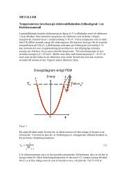
The electrical conductiv<strong>it</strong>y <strong>is</strong> schematically depicted in the figure below, where the different<br />
regions are indicated.<br />
One can also study the evolution <strong>of</strong> the Fermi level w<strong>it</strong>h temperature. We put the general<br />
expression for n, H, eq. (7.11), equal to our expressions above. In the low temperature region<br />
(4) we then obtain:<br />
μ = Eg-(Eg-Ed)/2 + 1/2 kBT ln(Nd /n0).<br />
It <strong>is</strong> seen that the Fermi level at absolute zero <strong>is</strong> s<strong>it</strong>uated half way between the donor levels<br />
and the conduction band edge. As the temperature incre<strong>as</strong>es the Fermi level will sink towards
the middle <strong>of</strong> the bandgap. At the crossover between regions (2) and (3) the expression for μ<br />
becomes in general complicated. In region (2) we again obtain a simple expression, namely<br />
μ = Eg - kBT ln(n0 /(Nd )).<br />
At very high temperatures the intrinsic s<strong>it</strong>uation <strong>is</strong> again attained. We have considered here ndoped<br />
semiconductors, but an analogous treatment can e<strong>as</strong>ily be developed for the p-type<br />
c<strong>as</strong>e.<br />
The temperature dependence <strong>of</strong> the Fermi level for n- and p-type semiconductors <strong>is</strong> depicted<br />
in the Figures below (adapted from Myers).
STUDY QUESTIONS<br />
1. What <strong>is</strong> the most important bandstructure features <strong>of</strong> semiconductors? How many valence<br />
and conduction bands do they have?<br />
2. What <strong>is</strong> the difference between a direct and an indirect bandgap?<br />
3. Consider optical absorption in semiconductors w<strong>it</strong>h a direct and indirect band gap. How <strong>is</strong><br />
wave vector and energy conserved in an indirect electronic trans<strong>it</strong>ion?<br />
4. What <strong>is</strong> the relation between the number<strong>of</strong> electrons and holes in an intrinsic<br />
semiconductor? Where <strong>is</strong> the chemical potential at T=0?<br />
5. One can dope a semiconductor w<strong>it</strong>h an impur<strong>it</strong>y (donor) having one electron more than the<br />
semiconductor. What happens to the extra electron? In which state and at which energy <strong>is</strong> <strong>it</strong><br />
s<strong>it</strong>uated in a band structure scheme?<br />
6. Do the same for acceptor doping (p-doping).<br />
7. Calculate the ionization energy for a donor electron w<strong>it</strong>h effective m<strong>as</strong>s 0.1 <strong>of</strong> the electron<br />
m<strong>as</strong>s and a dielectric perm<strong>it</strong>tiv<strong>it</strong>y <strong>of</strong> 10.<br />
8. What happens if a semiconductor <strong>is</strong> doped w<strong>it</strong>h equal amounts <strong>of</strong> both donors and<br />
acceptors?<br />
9. State the cond<strong>it</strong>ion <strong>of</strong> neutral<strong>it</strong>y for a donor doped semiconductor.<br />
10. How can you obtain a value <strong>of</strong> the band gap from a su<strong>it</strong>able plot <strong>of</strong> the electrical<br />
conductiv<strong>it</strong>y? Sketch!<br />
11. How can you obtain the ionization energy <strong>of</strong> a dopant from the same plot?<br />
12. How can you obtain the doping concentration if the mobil<strong>it</strong>y <strong>is</strong> known?