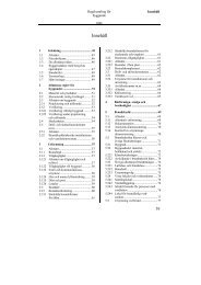
Lab 3: Getting Started with DRC, LVS, PEX
Lab 3: Getting Started with DRC, LVS, PEX
Lab 3: Getting Started with DRC, LVS, PEX

Create successful ePaper yourself
Turn your PDF publications into a flip-book with our unique Google optimized e-Paper software.
<strong>Lab</strong> 3: <strong>Getting</strong> <strong>Started</strong> <strong>with</strong> <strong>DRC</strong>, <strong>LVS</strong>,<br />
Last Modified Jan. 12, 2008<br />
<strong>PEX</strong><br />
INTRODUCTION: This lab exercise introduces how to verify the layout of<br />
my_inverter created in the last lab, using Mentor IC verification toolsets. This lab will<br />
cover:<br />
Design rules checking (<strong>DRC</strong>) <strong>with</strong> ICrules.<br />
Layout versus schematic (<strong>LVS</strong>) <strong>with</strong> ICtrace.<br />
Parasitic extraction (<strong>PEX</strong>) <strong>with</strong> ICextract.<br />
<strong>DRC</strong> <strong>with</strong> ICrules:All the other IC verification toolsets are integrated <strong>with</strong>in<br />
ICStation environment. ICrules is used for design rules checking (<strong>DRC</strong>).<br />
1) Generate Design viewpoint: in the Console window, type the following command to<br />
generate design viewpoint:<br />
adk_dve /home/vlsi/cad2008/cadxx/my_inverter/my_inverter<br />
This will generate the design viewpoint. The design viewpoint are used by different<br />
applications, for example, <strong>LVS</strong> view point. Although the different application's object is<br />
the same one created from Design Architect, their requested information is different<br />
between each other. These applications deal <strong>with</strong> the design object <strong>with</strong> different<br />
viewpoints. Just like a person, who is a teacher to his students, a father to his daughter<br />
and a son to his parents. We need to create different viewpoints for different applications.<br />
After back annotation, the design object will include the information from different<br />
viewpoints.<br />
2) start the IC Station by input :<br />
adk_ic &<br />
3) Open the MY_INV cell that you created in lab2 from<br />
/home/vlsi/cad2008/cadxx/physical_lib directory.<br />
4) Set your working directory by using the pull down menu, MGC>Location Map>Set<br />
Working Directory and enter: /home/vlsi/cad2008/cadxx/physical_lib<br />
5) Click on the ICrules item on the IC palette. You may have a look at which design<br />
rules will be checked, by selecting List>Checks. All the rules displayed in the dialog box<br />
are defined in the design rules file $ADK/technology/ic/process/ami05.rules. Select the<br />
rule you want to check and click OK. Click Cancel to close the window.
6) Select the pull-down menu MGC>Setup... to set sessions shown as left right tiling.<br />
Click OK.<br />
7) Open the transcript window by selecting MGC>Transcript>Show Transcript.<br />
8) Activate the layout window by clicking on the layout screen and click on the [Check]<br />
item on the IC Rules palette and press OK in the Check <strong>DRC</strong> box that pops up in the<br />
lower left corner of the layout window. You will see all the checking results shown in the<br />
transcript window.<br />
Figure 1: Design Rules Check Window<br />
9) If you got design rules violations, scan these violations by selecting Set Scan to<br />
[First], which is located on the palette window (which is only shown when the layout<br />
window is active) to see the first error, which is higlighted in the layout. It can be<br />
convenient to zoom in on the error to be able to correct it. Press [Next] until all errors are<br />
corrected.
At the bottom of the transcript a line such as (<strong>DRC</strong> compleated, Total Rule Checks:79;<br />
Total Results: 0: Total Original Geometries: 41 ... etc). The number beside Total Results<br />
signifies design Errors.<br />
There may be errors in this lab regarding VDD and GND connection. To solve this, you<br />
need to fully cover the VDD and GND <strong>with</strong> a Metal1 layer. Refer to <strong>Lab</strong> 2 for details on<br />
how to define this layer.<br />
Other common errors come from the space limitation violation.<br />
A) To edit your cell select the pull down menu File>Cell>Reserve.<br />
B) Correct the violations using layout editing techniques learned in <strong>Lab</strong> 2.<br />
C) <strong>DRC</strong> again (by repeating steps 8-9 above) until no violation is found,.<br />
D) Save your cell. File>Cell>Save Cell>Current Context.<br />
<strong>LVS</strong> using ICtrace (M): There exist two types of layout versus schematic<br />
(<strong>LVS</strong>) verifications, Direct and Mask. <strong>LVS</strong> compares the schematic connections you<br />
created in Design Architect to the net connections made in the IC Station.<br />
Direct mode compares the electrical connectivity at the current heiarchy and stores<br />
the connectivity information directly <strong>with</strong>in the cell. This mode allows for top down<br />
design where subcomponents may not be implemented yet. Direct mode views<br />
subcomponents from a "Black Box" perspective.<br />
Mask mode compares electrical connectivity of the entire ICgraph hierarchical<br />
layout <strong>with</strong> the connectivity of the source circuit. Mask mode is the most complete<br />
connectivity checking but on large designs it requires excessive time to extract at every<br />
heirarchy.<br />
1) If the active palette is still the ICrules palette, select Back to go back to IC<br />
Palette. Then select ICtrace (M) item.<br />
2) Select Logic>Open: from the ICtrace (M) palette and navigate to your<br />
/home/vlsi/cad2008/cadxx/my_inverter/my_inverter/lvs directory. Click OK<br />
This will open the schematic design viewpoint you created in Design Architect, lab 1.<br />
You can visually compare connections between the schematic and the layout, by selecting<br />
nets (interconnections) or instances (parts) in the schematic window. If the design does<br />
not open; choose File>logic>close and try again.<br />
3) Activate the layout window. Select the pull down menu File>logic>close to allow<br />
<strong>LVS</strong> to perform.<br />
4) Click on <strong>LVS</strong> in the ICtrace (M) palette. In the dialog box, it will automatically<br />
show the Report name as lvs.rep (if it doesn't automatically show, you need to input<br />
this). Select Source name <strong>with</strong><br />
/home/vlsi/cad2008/cadxx/my_inverter/my_inverter/lvs (design viewpoint file you<br />
created). Click OK.<br />
A) Click on the Setup <strong>LVS</strong>... button. In the Setup <strong>LVS</strong> window: change the<br />
following items Ground Names: VSS GND Recognize Gates : Yes and click OK.<br />
B) Run <strong>LVS</strong> by pressing [OK] in the <strong>LVS</strong> (Mask) dialog box.<br />
5) When the <strong>LVS</strong> check completes, select Report><strong>LVS</strong> from ICtrace (M)<br />
palette.(Activate layout window to see the ICtrace (M) palette)
If you see a cross symbol in the report file(Figure 2), which means that this <strong>LVS</strong> failed.<br />
The errors are listed below that cross symbol, you should look at them and correct your<br />
layout .<br />
Figure 2: Incorrect <strong>LVS</strong><br />
There are two errors you may have here - we use these errors to show you how to correct<br />
the <strong>LVS</strong>.
(1) In the schematic you designed in lab 1, we are using W =5 and L = 2, while in<br />
lab2 when you create the layout, we are using W=4 and L=2. Therefore, you need<br />
to change the transistor in the schematic that you created in lab 1 to W=4. To do<br />
this, after you open the schematic in Design Architecture, select the transistor, right<br />
click the mouse, select "Properties". You will see all the parameters related to the<br />
transistor. Select "Width = 5", click OK. and you will be asked to modify the<br />
property. Change the Value to 4.<br />
(2) Connect the "Bulk" terminal (the arrow terminal) of PMOS to VDD, and<br />
connect the Bulk terminal of NMOS to GND.<br />
(3) After you modifed the schematic, Check & Save and go to regenerate the<br />
design viewpoint. Type the following command in the Console.<br />
adk_dve /home/vlsi/cad2008/cadxx/my_inverter/my_inverter/my_inverter<br />
Exit and reopen IC station. Run <strong>LVS</strong> again, and check Report-><strong>LVS</strong> again, you should<br />
see a smiley face, which means your layout is correct now, otherwise repeat previous<br />
steps until you see the smiley.<br />
You may use cross probing and highlighting (activate the layout window choose<br />
Connectivity>Net>Highlight) to understand the relation between the layout and the<br />
schematic. When you select the net VSS in the schematic window, you may find that the<br />
polygon of P-well in the layout window is not highlighted, while the whole substrate is<br />
highlighted. This is because the p-well layer is not defined in the design rules.<br />
Figure 3: Correct Lvs
Post-layout Extraction using Calibre <strong>PEX</strong>:<br />
With the layout complete and passing <strong>LVS</strong> and <strong>DRC</strong>, it is time to extract the layout<br />
parasitic netlist. This will give you a spice netlist of your layout complete <strong>with</strong> resistance,<br />
parasitic capacitance and coupling capacitance. For the extraction process you will use<br />
Calibre Interactive - <strong>PEX</strong>.<br />
Before you run <strong>PEX</strong>, you need to generate the netlist. Got to ICTrace (M) from the IC<br />
Palettes, click on [Netlist]. In the pop-up window, input a name for the netlist :<br />
MY_INV_netlist, keep all the other setting as default and click OK This will generate<br />
netlist for your <strong>PEX</strong>.<br />
Step 1: In IC Stations menu bar, select Calibre -> Run <strong>PEX</strong>. In the pop-up window,<br />
input the Path to Calibre tree<br />
$CAL_HOME<br />
This will launch Calibre Interactive - <strong>PEX</strong>.
Step 2: If this is your first time running Calibre Interactive - <strong>PEX</strong> you will need to<br />
create a new runset so just click Cancel. If you have run Calibre before find the previous<br />
runset. This will simplify setting up Calibre.<br />
Step 3: Begin by clicking the Rules button and setting the rule file and working<br />
directory. The rule file should be of the form:<br />
$ADK/technology/ic/process/ami05.calibre.rules<br />
The Rules button should now be green.<br />
Step 4: Next click the Inputs button. The Layout tab should already be set correctly.<br />
Under the H-Cells tab, change the <strong>PEX</strong> x-cell file path to<br />
$ADK/technology/adk.hcell.<br />
Under "Netlist" tab, change the "Files" to be "MY_INV_netlist" that you generated.<br />
Step 5: Now select the Outputs button. At the top, the Extraction Type should be<br />
Transistor Level and you can choose one of the following types:<br />
RCC - Distributed RC network <strong>with</strong> coupling capacitors<br />
RC - Distributed RC network <strong>with</strong>out coupling capacitors<br />
C - Lumped net capacitance <strong>with</strong> coupling capacitors<br />
Select the first one: Distributed RC + coupling caps<br />
Step 6: In the Netlist tab you can setup the output format and file name. Choose DSPF as<br />
the Format and Use Names From: LAYOUT. You should also see there is a name for<br />
File: " MY_INV.pex.netlist ". You may change this file name to be<br />
"MY_INV.pex.netlist_DSPF" for you to remember that the output file is a DSPF<br />
format. Remember this output file name since you will need this output file for postlayout<br />
simulation.<br />
Step 7: Next choose Setup -> <strong>PEX</strong> Options from the menu bar. In the Netlist tab click<br />
the Ground node name: check box and enter GND. In the <strong>LVS</strong> Options tab set<br />
Recognize gates: to All. Also enter the following:<br />
Power nets: VDD<br />
Ground nets: GND<br />
Step 8: You should now be all set to perform the extraction so click Run <strong>PEX</strong>. If a pop<br />
up asks to overwrite the layout file click OK to ensure Calibre sees any recent changes to<br />
your layout.<br />
Step 9: When Calibre has completed the extraction a window will pop up showing the<br />
top level of the extracted netlist. Notice that there may be up to two additional netlists<br />
which will be included into the top level. The first will contain the RC networks and the<br />
second will contain the coupling capacitors.<br />
Step 10: Close IC station