Cyclone III Device Family Pin Connection Guidelines (PDF - Altera
Cyclone III Device Family Pin Connection Guidelines (PDF - Altera
Cyclone III Device Family Pin Connection Guidelines (PDF - Altera
Create successful ePaper yourself
Turn your PDF publications into a flip-book with our unique Google optimized e-Paper software.
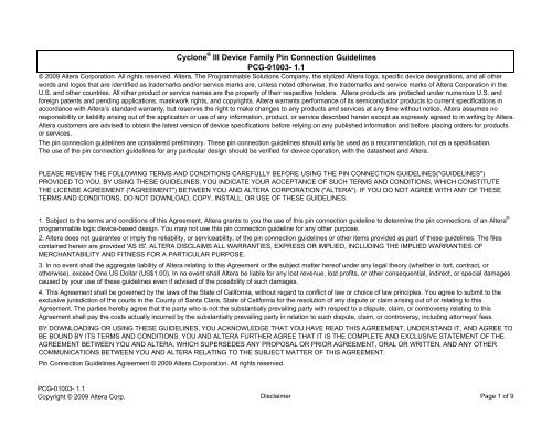
<strong>Cyclone</strong> ® <strong>III</strong> <strong>Device</strong> <strong>Family</strong> <strong>Pin</strong> <strong>Connection</strong> <strong>Guidelines</strong><br />
PCG-01003- 1.1<br />
© 2009 <strong>Altera</strong> Corporation. All rights reserved. <strong>Altera</strong>, The Programmable Solutions Company, the stylized <strong>Altera</strong> logo, specific device designations, and all other<br />
words and logos that are identified as trademarks and/or service marks are, unless noted otherwise, the trademarks and service marks of <strong>Altera</strong> Corporation in the<br />
U.S. and other countries. All other product or service names are the property of their respective holders. <strong>Altera</strong> products are protected under numerous U.S. and<br />
foreign patents and pending applications, maskwork rights, and copyrights. <strong>Altera</strong> warrants performance of its semiconductor products to current specifications in<br />
accordance with <strong>Altera</strong>’s standard warranty, but reserves the right to make changes to any products and services at any time without notice. <strong>Altera</strong> assumes no<br />
responsibility or liability arising out of the application or use of any information, product, or service described herein except as expressly agreed to in writing by <strong>Altera</strong>.<br />
<strong>Altera</strong> customers are advised to obtain the latest version of device specifications before relying on any published information and before placing orders for products<br />
or services.<br />
The pin connection guidelines are considered preliminary. These pin connection guidelines should only be used as a recommendation, not as a specification.<br />
The use of the pin connection guidelines for any particular design should be verified for device operation, with the datasheet and <strong>Altera</strong>.<br />
PLEASE REVIEW THE FOLLOWING TERMS AND CONDITIONS CAREFULLY BEFORE USING THE PIN CONNECTION GUIDELINES("GUIDELINES")<br />
PROVIDED TO YOU. BY USING THESE GUIDELINES, YOU INDICATE YOUR ACCEPTANCE OF SUCH TERMS AND CONDITIONS, WHICH CONSTITUTE<br />
THE LICENSE AGREEMENT ("AGREEMENT") BETWEEN YOU AND ALTERA CORPORATION ("ALTERA"). IF YOU DO NOT AGREE WITH ANY OF THESE<br />
TERMS AND CONDITIONS, DO NOT DOWNLOAD, COPY, INSTALL, OR USE OF THESE GUIDELINES.<br />
1. Subject to the terms and conditions of this Agreement, <strong>Altera</strong> grants to you the use of this pin connection guideline to determine the pin connections of an <strong>Altera</strong> ®<br />
programmable logic device-based design. You may not use this pin connection guideline for any other purpose.<br />
2. <strong>Altera</strong> does not guarantee or imply the reliability, or serviceability, of the pin connection guidelines or other items provided as part of these guidelines. The files<br />
contained herein are provided 'AS IS'. ALTERA DISCLAIMS ALL WARRANTIES, EXPRESS OR IMPLIED, INCLUDING THE IMPLIED WARRANTIES OF<br />
MERCHANTABILITY AND FITNESS FOR A PARTICULAR PURPOSE.<br />
3. In no event shall the aggregate liability of <strong>Altera</strong> relating to this Agreement or the subject matter hereof under any legal theory (whether in tort, contract, or<br />
otherwise), exceed One US Dollar (US$1.00). In no event shall <strong>Altera</strong> be liable for any lost revenue, lost profits, or other consequential, indirect, or special damages<br />
caused by your use of these guidelines even if advised of the possibility of such damages.<br />
4. This Agreement shall be governed by the laws of the State of California, without regard to conflict of law or choice of law principles. You agree to submit to the<br />
exclusive jurisdiction of the courts in the County of Santa Clara, State of California for the resolution of any dispute or claim arising out of or relating to this<br />
Agreement. The parties hereby agree that the party who is not the substantially prevailing party with respect to a dispute, claim, or controversy relating to this<br />
Agreement shall pay the costs actually incurred by the substantially prevailing party in relation to such dispute, claim, or controversy, including attorneys' fees.<br />
BY DOWNLOADING OR USING THESE GUIDELINES, YOU ACKNOWLEDGE THAT YOU HAVE READ THIS AGREEMENT, UNDERSTAND IT, AND AGREE TO<br />
BE BOUND BY ITS TERMS AND CONDITIONS. YOU AND ALTERA FURTHER AGREE THAT IT IS THE COMPLETE AND EXCLUSIVE STATEMENT OF THE<br />
AGREEMENT BETWEEN YOU AND ALTERA, WHICH SUPERSEDES ANY PROPOSAL OR PRIOR AGREEMENT, ORAL OR WRITTEN, AND ANY OTHER<br />
COMMUNICATIONS BETWEEN YOU AND ALTERA RELATING TO THE SUBJECT MATTER OF THIS AGREEMENT.<br />
<strong>Pin</strong> <strong>Connection</strong> <strong>Guidelines</strong> Agreement © 2009 <strong>Altera</strong> Corporation. All rights reserved.<br />
PCG-01003- 1.1<br />
Copyright © 2009 <strong>Altera</strong> Corp. Disclaimer Page 1 of 9
<strong>Cyclone</strong> ® <strong>III</strong> <strong>Device</strong> <strong>Family</strong> <strong>Pin</strong> <strong>Connection</strong> <strong>Guidelines</strong><br />
PCG-01003- 1.1 Note (1)<br />
You should create a Quartus ® II design, enter your device I/O assignments and compile the design. Quartus II will check your pin connections with respect to I/O assignment and placement rules to ensure proper device operation. These rules are dependent on<br />
device density, package, I/O assignments, voltage assignments, and other factors that are not fully described in this document or the device handbook.<br />
<strong>Cyclone</strong> <strong>III</strong> <strong>Device</strong>s <strong>Pin</strong> Name<br />
Supply and Reference <strong>Pin</strong>s<br />
<strong>Cyclone</strong> <strong>III</strong> LS <strong>Device</strong>s <strong>Pin</strong> Name<br />
<strong>Pin</strong> Type (1st, 2nd, &<br />
3rd Function) <strong>Pin</strong> Description <strong>Connection</strong> <strong>Guidelines</strong><br />
VCCINT VCCINT Power These are internal logic array voltage supply pins. All VCCINT pins must be connected to 1.2 V supply. Decoupling depends on the<br />
design decoupling requirements of the specific board. See Note 5.<br />
VCCIO[1..8] VCCIO[1..8] Power These are I/O supply voltage pins for banks 1 through 8. Each bank can Connect these pin to 1.2 V, 1.5 V, 1.8 V, 2.5 V, 3.0 V, or 3.3 V supplies,<br />
support a different voltage level. VCCIO supplies power to the input and depending on the I/O standard assigned to the I/O bank. Decoupling depends on<br />
output buffers for all I/O standards. VCCIO powers up the JTAG pins (TCK,<br />
TMS, TDI, and TDO) and the following configuration pins.. nCONFIG, DCLK,<br />
DATA[0..15], nCE, nCEO, nWE, nRESET, nOE, FLASH_nCE, nCSO, and<br />
CLKUSR.<br />
the design decoupling requirements of the specific board. See Note 5.<br />
VREFB[1..8]N[0..2] Note 2 VREFB[1..8]N[0..2] I/O Input reference voltage for each I/O bank. If a bank uses a voltagereferenced<br />
I/O standard for input operation, then these pins are used as the<br />
voltage-reference pins for the bank. If voltage reference I/O standards are<br />
not used in the bank, the VREF pins are available as user I/O pins.<br />
VCCA[1..4] Note 3 VCCA[1..4] Power Analog power for PLLs[1..4]. All VCCA pins must be powered and all VCCA<br />
pins must be powered up and powered down at the same time even if not all<br />
the PLLs are used. Designer is advised to keep isolated from other VCC for<br />
better jitter performance.<br />
VCCD_PLL[1..4] Note 3 VCCD_PLL[1..4] Power Digital power for PLLs[1..4]. The designer must power up these pins, even if<br />
the PLL is not used.<br />
NA VCCBAT Power Battery back-up power supply for design security volatile key register. The<br />
nominal voltage for this supply is 3.0 V.<br />
If VREF pins are not used, the designer should connect them to either the VCCIO<br />
of the I/O bank in which the pin resides or GND. Decoupling depends on the<br />
design decoupling requirements of the specific board. See Note 5. When VREF<br />
pins are used as I/O, they have higher capacitance than regular I/O pins which will<br />
slow the edge rates and affect I/O timing.<br />
The designer must connect these pins to 2.5 V, even if the PLL is not used. These<br />
pins must be powered up and powered down at the same time. Connect<br />
VCCA[1..4] pins together. VCCA supply to the chip should be isolated. See Note 6<br />
for details. See Note 7 for recommended decoupling.<br />
The designer must connect these pins to 1.2 V, even if the PLL is not used.<br />
Connect VCCD_PLL[1..4] pins together. VCCD_PLL supply to the chip should be<br />
isolated. See Note 6 for details. See Note 8 for recommended decoupling.<br />
Connect this pin to a 3.0 V non-volatile battery power source if using the volatile<br />
key. Its valid operating range is from 1.2 to 3.3-V. When not using the volatile key<br />
tie this to either 1.8-V, 2.5-V or 3.0-V power supply.<br />
RUP[1..4] RUP[1..4] I/O, Input Reference pins for on-chip termination (OCT) block in I/O banks 2, 4, 5, and When using OCT tie these pins to the required banks VCCIO through either a 25 Ω<br />
7. The external precision resistor RUP must be connected to the designated or 50 Ω resistor, depending on the desired I/O standard. When the device does<br />
RUP pin within the same bank when used. If the RUP pin is not used, this pin not use this dedicated input for the external precision resistor or as an I/O, it is<br />
can function as a regular I/O pin.<br />
recommended that the pin be connected to VCCIO of the bank in which the RUP<br />
pin resides or GND.<br />
RDN[1..4] RDN[1..4] I/O, Input Reference pins for on-chip termination (OCT) block in I/O banks 2, 4, 5, and<br />
7. The external precision resistor RDN must be connected to the designated<br />
RDN pin within the same bank when used. If the RDN pin is not used, this<br />
pin can function as a regular I/O pin.<br />
When using OCT tie these pins to GND through either a 25 Ω or 50 Ω resistor<br />
depending on the desired I/O standard. When the device does not use this<br />
dedicated input for the external precision resistor or as an I/O, it is recommended<br />
that the pin be connected to GND.<br />
GND GND Ground <strong>Device</strong> ground pins. All GND pins should be connected to the board GND plane.<br />
GNDA[1..4] Note 3 GNDA[1..4] Ground Ground for PLLs[1..4] and other analog circuits in the device. The designer can consider connecting the GNDA pins to the GND plane without<br />
isolating the analog ground plane on the board provided the digital GND plane(s)<br />
are stable, quiet, and with no ground bounce effect.<br />
NC NC No Connect No Connect. Do not connect these pins to any signal. These pins should be left unconnected,<br />
except when device migration requires a different connection to support different<br />
density devices.<br />
PCG-01003-1.1<br />
Copyright © 2009 <strong>Altera</strong> Corp. <strong>Pin</strong> <strong>Connection</strong> <strong>Guidelines</strong> Page 2 of 9
<strong>Cyclone</strong> ® <strong>III</strong> <strong>Device</strong> <strong>Family</strong> <strong>Pin</strong> <strong>Connection</strong> <strong>Guidelines</strong><br />
PCG-01003- 1.1 Note (1)<br />
You should create a Quartus ® II design, enter your device I/O assignments and compile the design. Quartus II will check your pin connections with respect to I/O assignment and placement rules to ensure proper device operation. These rules are dependent on<br />
device density, package, I/O assignments, voltage assignments, and other factors that are not fully described in this document or the device handbook.<br />
<strong>Pin</strong> Type (1st, 2nd, &<br />
3rd Function) <strong>Pin</strong> Description <strong>Connection</strong> <strong>Guidelines</strong><br />
<strong>Cyclone</strong> <strong>III</strong> <strong>Device</strong>s <strong>Pin</strong> Name<br />
Dedicated Configuration/JTAG <strong>Pin</strong>s<br />
<strong>Cyclone</strong> <strong>III</strong> LS <strong>Device</strong>s <strong>Pin</strong> Name<br />
DCLK DCLK Input (PS, FPP) DCLK is the dedicated configuration clock pin. In PS and FPP configuration,<br />
Output (AS, AP Note 13) DCLK is used to clock configuration data from an external source into<br />
<strong>Cyclone</strong> <strong>III</strong> device. In AS and AP Note 13 modes, DCLK is an output from<br />
the <strong>Cyclone</strong> <strong>III</strong> device that provides timing for the configuration interface.<br />
DATA0 DATA0 Input (PS,FPP,AS)<br />
Bidirectional open-drain<br />
(AP Note 13)<br />
Dedicated configuration data input pin. In serial configuration modes, bit-wide<br />
configuration data is received through this pin. In AS mode, DATA0 has an<br />
internal pull-up resistor that is always active. After AS configuration, DATA0<br />
is a dedicated input pin with optional user control. After PS or PP<br />
configuration, DATA0 is available as a user I/O pin and the state of this pin<br />
depends on the Dual-Purpose <strong>Pin</strong> settings. After AP Note 13 configuration,<br />
DATA0 is a dedicated bidirectional pin with optional user control.<br />
MSEL[0..3] MSEL[0..3] Input Configuration input pins that set the <strong>Cyclone</strong> <strong>III</strong> device configuration scheme.<br />
Some of the smaller devices or package options do not support the AP Note<br />
13 flash programming and do not have the MSEL3 pin.<br />
nCE nCE Input Dedicated active-low chip enable. When nCE is low, the device is enabled.<br />
When nCE is high, the device is disabled.<br />
nCONFIG nCONFIG Input Dedicated configuration control input. Pulling this pin low during user-mode<br />
will cause the FPGA to lose its configuration data, enter a reset state and tristate<br />
all I/O pins. Returning this pin to a logic high level will initiate<br />
reconfiguration.<br />
CONF_DONE CONF_DONE Bidirectional<br />
(open-drain)<br />
nSTATUS nSTATUS Bidirectional<br />
(open-drain)<br />
This is a dedicated configuration status pin. As a status output, the<br />
CONF_DONE pin drives low before and during configuration. Once all<br />
configuration data is received without error and the initialization cycle starts,<br />
CONF_DONE is released. As a status input, CONF_DONE goes high after<br />
all data is received. Then the device initializes and enters user mode.<br />
This is a dedicated configuration status pin. The FPGA drives nSTATUS low<br />
immediately after power-up and releases it after POR time. As a status<br />
output, the nSTATUS is pulled low if an error occurs during configuration. As<br />
a status input, the device enters an error state when nSTATUS is driven low<br />
by an external source during configuration or initialization.<br />
TCK TCK Input Dedicated JTAG input pin. The JTAG circuitry can be disabled by connecting<br />
TCK to GND.<br />
TMS TMS Input Dedicated JTAG input pin. The JTAG circuitry can be disabled by<br />
connecting TMS to VCC.<br />
DCLK should not be left floating. In JTAG configuration and schemes that use an<br />
external host, designer should drive it high or low, whichever is more convenient<br />
on the board. In AS and AP Note 13 mode, the DCLK has an internal pull-up<br />
resistor (typically 25-KΩ) that is always active.<br />
If you are using a serial configuration device in AS configuration mode, you must<br />
connect a 25-Ω series resistor at the near end of the serial configuration device for<br />
the DATA0. If DATA0 is not used, it should be driven high or low, whichever is<br />
more convenient on the board.<br />
These pins are internally connected to 5-KΩ resistor to GND. Do not leave these<br />
pins floating. When these pins are unused connect them to GND. Depending on<br />
the configuration scheme used, these pins should be tied to VCCA or GND. Refer<br />
to Chapter 9 of <strong>Cyclone</strong> <strong>III</strong> <strong>Device</strong> <strong>Family</strong> Handbook: Configuration, Design<br />
Security, and Remote System Upgrades in <strong>Cyclone</strong> <strong>III</strong> <strong>Device</strong>s. If only JTAG<br />
configuration is used, then connect these pins to GND.<br />
In multi-device configuration, nCE of the first device is tied directly to GND while<br />
its nCEO pin drives the nCE of the next device in the chain. In single device<br />
configuration, nCE is tied directly to GND. The nCE pin must also be held low for<br />
successful JTAG programming of the device. If you are combining JTAG and AS<br />
configuration schemes, then the nCE should be tied to GND through a 10-K Ω<br />
resistor.<br />
If you are using PS configuration scheme with a download cable, connect this pin<br />
through a 10-KΩ resistor to VCCA. For other configuration schemes, if this pin is<br />
not used, this pin must be connected directly or through a 10-K Ω resistor to<br />
VCCIO.<br />
This pin is not available as a user I/O pin. CONF_DONE should be pulled high by<br />
an external 10-KΩ pull-up resistor.<br />
This pin is not available as a user I/O pin. nSTATUS should be pulled high by an<br />
external 10-KΩ pull-up resistor.<br />
Connect this pin to a 1-KΩ resistor to GND.<br />
When interfacing with 2.5 V/3.0 V/3.3 V configuration voltage standards, connect<br />
this pin through a 10-KΩ resistor to VCCA. For configuration voltage of 1.5 V and<br />
1.8 V, connect this pin through a 10-K Ω resistor to VCCIO supply instead. See<br />
Note 10.<br />
PCG-01003-1.1<br />
Copyright © 2009 <strong>Altera</strong> Corp. <strong>Pin</strong> <strong>Connection</strong> <strong>Guidelines</strong> Page 3 of 9
<strong>Cyclone</strong> ® <strong>III</strong> <strong>Device</strong> <strong>Family</strong> <strong>Pin</strong> <strong>Connection</strong> <strong>Guidelines</strong><br />
PCG-01003- 1.1 Note (1)<br />
You should create a Quartus ® II design, enter your device I/O assignments and compile the design. Quartus II will check your pin connections with respect to I/O assignment and placement rules to ensure proper device operation. These rules are dependent on<br />
device density, package, I/O assignments, voltage assignments, and other factors that are not fully described in this document or the device handbook.<br />
<strong>Cyclone</strong> <strong>III</strong> <strong>Device</strong>s <strong>Pin</strong> Name <strong>Cyclone</strong> <strong>III</strong> LS <strong>Device</strong>s <strong>Pin</strong> Name<br />
<strong>Pin</strong> Type (1st, 2nd, &<br />
3rd Function) <strong>Pin</strong> Description <strong>Connection</strong> <strong>Guidelines</strong><br />
TDI TDI Input Dedicated JTAG input pin. The JTAG circuitry can be disabled by connecting When interfacing with 2.5 V/3.0 V/3.3 V configuration voltage standards, connect<br />
TDI to VCC.<br />
this pin through a 10-KΩ resistor to VCCA. For configuration voltage of 1.5 V and<br />
1.8 V, connect this pin through a 10-K Ω resistor to VCCIO supply instead. See<br />
Note 10.<br />
TDO<br />
Clock and PLL <strong>Pin</strong>s<br />
TDO Output Dedicated JTAG output pin. If the TDO pin is not used, leave this pin unconnected.<br />
CLK[0,2,4,6,9,11,13,15], DIFFCLK_[0..7]p CLK[0,2,4,6,9,11,13,15], DIFFCLK_[0..7]p Clock, Input Dedicated global clock input pins that can also be used for the positive Connect unused pins to GND. See Note 9.<br />
Note 4<br />
terminal inputs for differential global clock input or user input pins. These<br />
dedicated clock pins do not support programmable weak pull-up resistor.<br />
CLK[1,3,5,7,8,10,12,14], DIFFCLK_[0..7]n<br />
Note 4<br />
CLK[1,3,5,7,8,10,12,14], DIFFCLK_[0..7]n Clock, Input Dedicated global clock input pins that can also be used for the negative<br />
terminal inputs for differential global clock input or user input pins. These<br />
dedicated clock pins do not support programmable weak pull-up resistor.<br />
Connect unused pins to GND. See Note 9.<br />
PLL[1..4]_CLKOUTp Note 3 PLL[1..4]_CLKOUTp I/O, Output Optional positive terminal for external clock outputs from PLL [1..4]. These<br />
pins can be assigned to single-ended or differential I/O standards if it is being<br />
fed by a PLL output.<br />
Connect unused pins to GND. See Note 9.<br />
PLL[1..4]_CLKOUTn Note 3 PLL[1..4]_CLKOUTn I/O, Output Optional negative terminal for external clock outputs from PLL[1..4]. These<br />
pins can be assigned to single-ended or differential I/O standards if it is being<br />
fed by a PLL output.<br />
Connect unused pins to GND. See Note 9.<br />
Optional/Dual-Purpose Configuration <strong>Pin</strong>s<br />
nCEO nCEO I/O, Output (open-drain)<br />
FLASH_nCE, nCSO nCSO I/O, Output(AS,<br />
AP Note 13)<br />
DATA1, ASDO DATA1, ASDO Input (FPP)<br />
Output (AS)<br />
Bidirectional open-drain<br />
(AP Note 13)<br />
Output that drives low when device configuration is complete. During multi-device configuration, this pin feeds a subsequent device’s nCE pin<br />
and must be pulled high to VCCIO by an external 10-KΩ pull-up resistor. During<br />
single device configuration and for the last device in multi-device configuration,<br />
this pin can be left floating or used as a user I/O after configuration.<br />
This pin functions as FLASH_nCE in AP Note13 mode, and nCSO in<br />
AS mode. This pin has an internal pull-up resistor that is<br />
always active.<br />
nCSO: Output control signal from the <strong>Cyclone</strong> <strong>III</strong> device to the serial<br />
configuration device in AS mode that enables the configuration device.<br />
FLASH_nCE: Output control signal from the <strong>Cyclone</strong> <strong>III</strong> device<br />
to the parallel flash in AP Note 13 mode that enables the flash.<br />
This pin functions as DATA1 in PS and FPP modes, and as ASDO in AS<br />
mode.<br />
DATA1: Data input in non-AS mode. Byte-wide or word-wide configuration<br />
data is presented to the target device on DATA[0..7] or DATA[0..15]<br />
respectively.<br />
In PS configuration scheme, DATA1 functions as user I/O pin during<br />
configuration, which means it is tri-stated. After FPP configuration, DATA1 is<br />
available as a user I/O pin and the state of this pin depends on the Dual-<br />
Purpose <strong>Pin</strong> settings.<br />
ASDO: Control signal from the <strong>Cyclone</strong> <strong>III</strong> device to the serial configuration<br />
device in AS mode used to read out configuration data. In AS mode, this<br />
ASDO pin has an internal pull-up resistor that is always active. After AS<br />
configuration, this pin is a dedicated output pin with optional user control.<br />
When not programming the device in AS mode, nCSO is not used. Similarly,<br />
FLASH_nCE is not used when not programming the device in AP Note 13 mode. If<br />
the pin is not used as an I/O then it is recommended to leave the pin unconnected.<br />
When not programming the device in AS mode, this pin is available as a user I/O<br />
pin. If the pin is not used as an I/O then it is recommended to leave the pin<br />
unconnected.<br />
PCG-01003-1.1<br />
Copyright © 2009 <strong>Altera</strong> Corp. <strong>Pin</strong> <strong>Connection</strong> <strong>Guidelines</strong> Page 4 of 9
<strong>Cyclone</strong> ® <strong>III</strong> <strong>Device</strong> <strong>Family</strong> <strong>Pin</strong> <strong>Connection</strong> <strong>Guidelines</strong><br />
PCG-01003- 1.1 Note (1)<br />
You should create a Quartus ® II design, enter your device I/O assignments and compile the design. Quartus II will check your pin connections with respect to I/O assignment and placement rules to ensure proper device operation. These rules are dependent on<br />
device density, package, I/O assignments, voltage assignments, and other factors that are not fully described in this document or the device handbook.<br />
<strong>Cyclone</strong> <strong>III</strong> <strong>Device</strong>s <strong>Pin</strong> Name <strong>Cyclone</strong> <strong>III</strong> LS <strong>Device</strong>s <strong>Pin</strong> Name<br />
<strong>Pin</strong> Type (1st, 2nd, &<br />
3rd Function) <strong>Pin</strong> Description <strong>Connection</strong> <strong>Guidelines</strong><br />
DATA[2..7] DATA[2..7] Inputs (FPP)<br />
Data inputs. Byte-wide or word-wide configuration data is presented to the When not programming the device in AS mode, this pin is available as a user I/O<br />
Bidirectional (AP Note target device on DATA [0..7] or DATA [0..15] respectively.<br />
pin. If the pin is not used as an I/O then it is recommended to tie this pin to<br />
13)<br />
In AS or PS configuration scheme, they function as user I/O pins during<br />
configuration, which means they are tri-stated.<br />
After FPP configuration, DATA [2..7] are available as user I/O pins and the<br />
state of these pins depends on the Dual-Purpose <strong>Pin</strong> settings.<br />
VCCIO, GND, or leave the pin unconnected.<br />
DATA[8..15] NA Bidirectional (AP Note<br />
13)<br />
In the PS, FPP, or AS configuration scheme, they function as user I/O pins<br />
during configuration, which means they are tri-stated.<br />
After AP Note 13 configuration, DATA[8..15] are dedicated bidirectional pins<br />
with optional user control.<br />
PADD[0..23] NA Output (AP Note 13) 24-bit address bus from the <strong>Cyclone</strong> <strong>III</strong> device to the parallel flash in AP Note<br />
13 mode.<br />
When not programming the device in AP Note 13 mode, these pins are available<br />
as user I/O pins. If these pins are not used as I/Os, then it is recommended to tie<br />
this pin to VCCIO, GND, or leave the pin unconnected.<br />
When not programming the device in AP Note 13 mode, these pins are available<br />
as user I/O pins. If these pins are not used as I/Os, then it is recommended to tie<br />
this pin to VCCIO, GND or leave the pin unconnected.<br />
nRESET NA Output (AP Note13) Active-low reset output. Driving the nRESET pin low resets the parallel flash. When not programming the device in AP Note 13 mode, nRESET is not used and<br />
is available as a user I/O pin. If the pin is not used as an I/O then it is<br />
recommended to tie this pin to VCCIO, GND or leave the pin unconnected.<br />
nAVD NA Output (AP Note 13) Active-low address valid output. Driving the nAVD pin low during read or<br />
write operation indicates to the parallel flash that valid address is present on<br />
the PADD[0..23] address bus.<br />
nOE NA Output (AP Note 13) Active-low output enable to the parallel flash. Driving the nOE pin low during<br />
read operation enables the parallel flash outputs (DATA[0..15] and RDY).<br />
nWE NA Output (AP Note 13) Active-low write enable to the parallel flash. Driving the nWE pin low during<br />
write operation indicates to the parallel flash that data on the DATA[0..15]<br />
bus is valid.<br />
RDY NA Output (AP Note13) Control signal (WAIT) from the parallel flash is connected to this pin in the<br />
<strong>Cyclone</strong> <strong>III</strong> device to indicate when synchronous data is ready on the data<br />
bus.<br />
CRC_ERROR CRC_ERROR I/O, Output Active high signal that indicates that the error detection circuit has detected<br />
errors in the configuration SRAM bits. This pin is optional and is used when<br />
the CRC error detection circuit is enabled.<br />
DEV_CLRn DEV_CLRn I/O (when option off),<br />
Input (when option on)<br />
DEV_OE DEV_OE I/O (when option off),<br />
Input (when option on)<br />
Optional chip-wide reset pin that allows you to override all clears on all<br />
device registers. When this pin is driven low, all registers are cleared; when<br />
this pin is driven high, all registers behave as programmed. The DEV_CLRn<br />
pin does not affect JTAG boundary-scan or programming operations. This<br />
pin is enabled by turning on the Enable device-wide reset (DEV_CLRn)<br />
option in the Quartus II software.<br />
When not programming the device in AP Note 13 mode, nAVD is not used and is<br />
available as a user I/O pin. If the pin is not used as an I/O then it is recommended<br />
to tie this pin to VCCIO, GND or leave the pin unconnected.<br />
When not programming the device in AP Note 13 mode, nOE is not used and is<br />
available as a user I/O pin. If the pin is not used as an I/O then it is recommended<br />
to tie this pin to VCCIO, GND or leave the pin unconnected.<br />
When not programming the device in AP Note 13 mode, nWE is not used and is<br />
available as a user I/O pin. If the pin is not used as an I/O then it is recommended<br />
to tie this pin to VCCIO, GND, or leave the pin unconnected.<br />
The current implementation for AP Note 13 configuration ignores the RDY pin.<br />
However it is highly recommended to connect this pin to the AP Note 13 flash.<br />
When the CRC error detection circuitry is disabled and when this pin is not used<br />
as an I/O then it is recommended to tie this pin to VCCIO, GND or leave the pin<br />
unconnected.<br />
When the input DEV_CLRn is not used and this pin is not used as an I/O then it is<br />
recommended to tie this pin to VCCIO, GND, or leave the pin unconnected.<br />
Optional pin that allows you to override all tri-states on the device. When this When the input DEV_OE is not used and this pin is not used as an I/O then it is<br />
pin is driven low, all I/O pins are tri-stated; when this pin is driven high, all I/O recommended to tie this pin to VCCIO, GND, or leave the pin unconnected.<br />
pins behave as defined in the design. This pin is enabled by turning on the<br />
Enable device-wide output enable (DEV_OE) option in the Quartus II<br />
software.<br />
PCG-01003-1.1<br />
Copyright © 2009 <strong>Altera</strong> Corp. <strong>Pin</strong> <strong>Connection</strong> <strong>Guidelines</strong> Page 5 of 9
<strong>Cyclone</strong> ® <strong>III</strong> <strong>Device</strong> <strong>Family</strong> <strong>Pin</strong> <strong>Connection</strong> <strong>Guidelines</strong><br />
PCG-01003- 1.1 Note (1)<br />
You should create a Quartus ® II design, enter your device I/O assignments and compile the design. Quartus II will check your pin connections with respect to I/O assignment and placement rules to ensure proper device operation. These rules are dependent on<br />
device density, package, I/O assignments, voltage assignments, and other factors that are not fully described in this document or the device handbook.<br />
<strong>Cyclone</strong> <strong>III</strong> <strong>Device</strong>s <strong>Pin</strong> Name <strong>Cyclone</strong> <strong>III</strong> LS <strong>Device</strong>s <strong>Pin</strong> Name<br />
<strong>Pin</strong> Type (1st, 2nd, &<br />
3rd Function) <strong>Pin</strong> Description <strong>Connection</strong> <strong>Guidelines</strong><br />
INIT_DONE INIT_DONE I/O, Output<br />
This is a dual-purpose status pin and can be used as an I/O pin when not Connect this pin to a 10-KΩ resistor to VCCIO.<br />
(open-drain)<br />
enabled as INIT_DONE. When enabled, a transition from low to high at the<br />
pin indicates when the device has entered user mode. If the INIT_DONE<br />
output is enabled, the INIT_DONE pin cannot be used as a user I/O pin after<br />
configuration. This pin is enabled by turning on the Enable INIT_DONE<br />
output option in the Quartus II software.<br />
CLKUSR CLKUSR I/O, Input Optional user-supplied clock input. Synchronizes the initialization of one or<br />
more devices. If this pin is not enabled for use as a user-supplied<br />
configuration clock, it can be used as a user I/O pin. This pin is enabled by<br />
turning on the Enable user-supplied start-up clock (CLKUSR) option in the<br />
Quartus II software.<br />
Dual-Purpose Differential & External Memory Interface <strong>Pin</strong>s<br />
DIFFIO_[L,R,T,B][0..61][n,p] Note 11 DIFFIO_[L,R,T,B][0..47][n,p] Note 11 I/O, TX/RX channel Dual-purpose differential transmitter/receiver channels. These channels can<br />
be used for transmitting/receiving LVDS compatible signals. <strong>Pin</strong>s with a "p"<br />
suffix carry the positive signal for the differential channel. <strong>Pin</strong>s with an "n"<br />
suffix carry the negative signal for the differential channel. If not used for<br />
differential signaling, these pins are available as user I/O pins.<br />
DQS[0..5][L,R,T,B]/CQ[1,3,5][L,R,T,B][#],<br />
DPCLK[0..11] Note 12<br />
DQS[0..5][L,R,T,B]/CQ[1,3,5][L,R,T,B][#],<br />
CDPCLK[0..7] Note 12<br />
DQS[0..5][L,R,T,B]/CQ[1,3,5][L,R,T,B][#],<br />
DPCLK[0..11] Note 12<br />
DQS[0..5][L,R,T,B]/CQ[1,3,5][L,R,T,B][#],<br />
CDPCLK[0..7] Note 12<br />
I/O, DQS/CQ,DPCLK Dual-purpose DPCLK/DQS pins can connect to the global clock network for<br />
high fan-out control signals such as clocks, asynchronous clears, presets<br />
and clock enables. It can also be used as optional data strobe signal for use<br />
in external memory interfacing. These pins drive to dedicated DQS phase<br />
shift circuitry, which allows fine tune of the phase shift for input clocks or<br />
strobes to properly align clock edges needed to capture data.<br />
I/O, DQS/CQ,CDPCLK Dual-purpose CDPCLK/DQS pins can connect to the global clock network for<br />
high fan-out control signals such as clocks, asynchronous clears, presets,<br />
and clock enables. Only one of the two CDPCLK in each corner can feed the<br />
clock control block at a time. The other pin can be used as general-purpose<br />
I/O pin. The CDPCLK signals incur more delay to the clock block control<br />
because they are multiplexed before driving into the clock block control. It<br />
can also be used as optional data strobe signal for use in external memory<br />
interfacing. These pins drive to dedicated DQS phase shift circuitry, which<br />
allows fine tune of the phase shift for input clocks or strobes to properly align<br />
clock edges needed to capture data.<br />
If the CLKUSR pin is not used as a configuration clock input and the pin is not<br />
used as an I/O then it is recommended to connect this pin to GND.<br />
When these I/O pins are not used they can be tied to the VCCIO of the bank they<br />
reside in or GND. See Note 9.<br />
When these I/O pins are not used they can be tied to the VCCIO of the bank they<br />
reside in or GND. See Note 9.<br />
When these I/O pins are not used they can be tied to the VCCIO of the bank they<br />
reside in or GND. See Note 9.<br />
DQ[0..5][L,R,T,B] Note 12 DQ[0..5][L,R,T,B][0..35] Note 12 I/O, DQ Optional data signal for use in external memory interface. When these I/O pins are not used they can be tied to the VCCIO of the bank they<br />
reside in or GND. See Note 9.<br />
DM[0..5][L,R,B,T][0..1]/BWS#[0..5][L,R,T,B] DM[0..5][L,R,B,T][0..1]/BWS#[0..5][L,R,T,B][0..3] I/O, DM/BWS# The data mask pins are only required when writing to DDR SDRAM and<br />
DDR2 SDRAM devices. QDRII SRAM devices use the BWS signal to select<br />
the byte to be written into memory. A low signal on the DM/BWS# pin<br />
indicates that the write is valid. Driving the DM/BWS# pin high results in the<br />
memory masking the DQ signals.<br />
When these I/O pins are not used they can be tied to the VCCIO of the bank they<br />
reside in or GND. See Note 9.<br />
PCG-01003-1.1<br />
Copyright © 2009 <strong>Altera</strong> Corp. <strong>Pin</strong> <strong>Connection</strong> <strong>Guidelines</strong> Page 6 of 9
<strong>Cyclone</strong> ® <strong>III</strong> <strong>Device</strong> <strong>Family</strong> <strong>Pin</strong> <strong>Connection</strong> <strong>Guidelines</strong><br />
PCG-01003- 1.1 Note (1)<br />
You should create a Quartus ® II design, enter your device I/O assignments and compile the design. Quartus II will check your pin connections with respect to I/O assignment and placement rules to ensure proper device operation. These rules are dependent on<br />
device density, package, I/O assignments, voltage assignments, and other factors that are not fully described in this document or the device handbook.<br />
<strong>Cyclone</strong> <strong>III</strong> <strong>Device</strong>s <strong>Pin</strong> Name <strong>Cyclone</strong> <strong>III</strong> LS <strong>Device</strong>s <strong>Pin</strong> Name<br />
<strong>Pin</strong> Type (1st, 2nd, &<br />
3rd Function) <strong>Pin</strong> Description <strong>Connection</strong> <strong>Guidelines</strong><br />
<strong>Pin</strong>s Used to Turn On the Security Boundary Between I/O Banks<br />
NA B1 Note 14 I/O, Power, Ground <strong>Pin</strong>s used for setting up the security boundary for TDI, TDO and DATA0. To guarantee physical I/O separation of the JTAG, B1 labeled I/O pins should be<br />
connected to GND. Other B1 labeled pin such as VCCIO and GND pins should<br />
remain their initial function i.e VCCIO pin should remain connected to the power<br />
supply and GND pin should remain connected to ground.<br />
NA B1_B2, B2_B3, B3_B4, B4_B5, B5_B6, B6_B7,<br />
B7_B8, B8_B1 Note 15<br />
I/O, Power, Ground Physical pins that are used to turn on the security boundary between the I/O<br />
banks that is specified. For example: B1 for Bank 1 and B2 for Bank 2.<br />
Legend:<br />
Shaded cells indicate pins that are used in AP configuration mode for <strong>Cyclone</strong> <strong>III</strong> <strong>Device</strong>s and other configuration modes (except AP configuration mode) in <strong>Cyclone</strong> <strong>III</strong> LS <strong>Device</strong>s.<br />
When the I/O pins are used to turn on the security boundary between the I/O<br />
banks, the I/O pins must be connected to GND. The VCCIO and GND pins used to<br />
turn on the security boundary between the I/O banks should remain their initial<br />
function i.e VCCIO pin should remain connected to the power supply and GND pin<br />
should remain connected to ground.<br />
Notes:<br />
(1) This pin connection guideline is created based on the largest device density that is EP3C120F780 for <strong>Cyclone</strong> <strong>III</strong> <strong>Device</strong>s and EP3CLS200F780 for <strong>Cyclone</strong> <strong>III</strong> LS <strong>Device</strong>s.<br />
(2) EP3C5 and EP3C10 only support VREFB[1..8]N0.<br />
(3) EP3C5 and EP3C10 only have PLL(1 & 2). EP3C16 and other larger densities have PLL (1,2,3, and 4).<br />
(4) The number of dedicated global clocks for each device density is different. EP3C5 and EP3C10 support four dedicated clock pins on the left and right sides of the device, that can drive a total of 10 global clock networks. EP3C16 and other larger densities support four dedicated clock<br />
pins on each side of the device that can drive a total of 20 global clock networks.<br />
(5) Capacitance values for the power supply decoupling capacitors should be selected after consideration of the amount of power needed to supply over the frequency of operation of the particular circuit being decoupled. A target impedance for the power plane should be calculated based<br />
on current draw and voltage drop requirements of the device/supply. The power plane should then be decoupled using the appropriate number of capacitors. On-board capacitors do not decouple higher than 100 MHz due to “Equivalent Series Inductance” of the mounting of the packages.<br />
Proper board design techniques such as interplane capacitance with low inductance should be considered for higher frequency decoupling. To assist in decoupling analysis, <strong>Altera</strong>'s "Power Distribution Network (PDN) Design Tool" serves as an excellent decoupling analysis tool. The PDN<br />
design tool can be obtained at<br />
Power Distribution Network Design Tool.<br />
(6) Use seperate power island for VCCA and VCCD_PLL. PLL power supply may originate from another plane on the board but must be isolated using a ferrite bead or other equivalent methods. If using a ferrite bead, choose an 0402 package with low DC resistance, higher current rating<br />
than the maximum steady state current for the supply it is connected to(VCCA or VCCD_PLL) and high impedance at 100 MHz.<br />
(7) The VCCA power island can be decoupled with a combination of decoupling capacitors. Please refer to the<br />
Power Distribution Network Design Tool<br />
to determine the decoupling capacitors value. Use 0402 package for 0.1 uF and smaller capacitors for lower mounting inductance. Place 0.1 uF and smaller capacitors as close to the device as possible. On-board capacitors do not decouple higher than 100 MHz due to “Equivalent Series<br />
Inductance” of the mounting of the packages. Proper board design techniques such as interplane capacitance with low inductance should be considered for higher frequency decoupling. To minimize impact on jitter, a 20 mV ripple voltage was used in the analysis for VCCA decoupling.<br />
Refer to Figure for decoupling capacitor placement guidelines. Figure depicts symbolic representation of decoupling scheme and not the exact layout.<br />
(8) The VCCD_PLL power island can be decoupled with a combination of decoupling capacitors. Please refer to the “Power Distribution Network Design Tool” at<br />
Power Distribution Network Design Tool<br />
to determine the decoupling capacitors value. Place 0.1 uF and smaller capacitors as close to the device as possible. On-board capacitors do not decouple higher than 100 MHz due to “Equivalent Series Inductance” of the mounting of the packages. Proper board design techniques such as<br />
interplane capacitance with low inductance should be considered for higher frequency decoupling. To minimize impact on jitter, a 20 mV ripple voltage was used in the analysis for VCCD_PLL decoupling. Refer to Figure for decoupling capacitor placement guidelines. Figure depicts<br />
symbolic representation of decoupling scheme and not the exact layout.<br />
(9) The unused pins must be connected as specified in the Quartus II software settings. The default Quartus II setting for unused pins is 'As inputs tri-stated with weak pull-up resistors', unless for specific pins that Quartus II software connects them to GND automatically. To change the<br />
setting, go to 'Assignments', then '<strong>Device</strong>'. Click on '<strong>Device</strong> & <strong>Pin</strong> options' dialog box and go to 'Unused <strong>Pin</strong>s' tab. You may choose the desired setting from the 'Reserve all unused pins' drop down list.<br />
(10) You must follow specific requirements when interfacing <strong>Cyclone</strong> <strong>III</strong> device with 2.5 V/3.0 V/3.3 V configuration voltage standards. All I/O inputs must maintain a maximum AC voltage of 4.1 V. Refer to Configuration and JTAG <strong>Pin</strong> I/O Requirements of Chapter 9: Configuration, Design<br />
Security, and Remote System Upgrades in <strong>Cyclone</strong> <strong>III</strong> <strong>Device</strong>s.<br />
(11) The differential TX/RX channels for each device density and package is different. Please refer to the <strong>Cyclone</strong> <strong>III</strong> <strong>Device</strong> <strong>Family</strong> Handbook Chapter 7. High-Speed Differential Interfaces in <strong>Cyclone</strong> <strong>III</strong> <strong>Device</strong>s.<br />
(12) For details about the DQ and DQS bus modes support in different device densities, refer to the <strong>Cyclone</strong> <strong>III</strong> <strong>Device</strong> <strong>Family</strong> Handbook Chapter 8. External Memory Interfaces in <strong>Cyclone</strong> <strong>III</strong> <strong>Device</strong>s.<br />
(13) Configuration in AP mode is only supported in <strong>Cyclone</strong> <strong>III</strong> <strong>Device</strong>s and not in <strong>Cyclone</strong> <strong>III</strong> LS <strong>Device</strong>s.<br />
(14) B1 is not the pin name in the <strong>Cyclone</strong> <strong>III</strong> LS <strong>Device</strong> family but rather the labeled named used for the I/O, power and ground pins used to form the security boundary for TDI, TDO, and DATA0 pin. Please refer to <strong>Cyclone</strong> <strong>III</strong> LS <strong>Device</strong>s <strong>Pin</strong>-out file for more information.<br />
(15) B1_B2, B2_B3, B3_B4, B4_B5, B5_B6, B6_B7, B7_B8, B8_B1 are not the pin name in the <strong>Cyclone</strong> <strong>III</strong> LS <strong>Device</strong> family but rather the labeled name used for I/O, power, or ground pins used to form the security boundary to separate the banks. Please refer to the <strong>Cyclone</strong> <strong>III</strong> LS <strong>Device</strong>s<br />
<strong>Pin</strong>-out files for more information.<br />
PCG-01003-1.1<br />
Copyright © 2009 <strong>Altera</strong> Corp. <strong>Pin</strong> <strong>Connection</strong> <strong>Guidelines</strong> Page 7 of 9
Figure 1: PLL Power Decoupling Diagram<br />
<strong>Cyclone</strong> ® <strong>III</strong> <strong>Device</strong> <strong>Family</strong> <strong>Pin</strong> <strong>Connection</strong> <strong>Guidelines</strong><br />
PCG-01003- 1.1<br />
PCG-01003- 1.1<br />
Copyright © 2009 <strong>Altera</strong> Corp. PLL Power Decoupling Page 8 of 9
<strong>Cyclone</strong> ® <strong>III</strong> <strong>Device</strong> <strong>Family</strong> <strong>Pin</strong> <strong>Connection</strong> <strong>Guidelines</strong><br />
PCG-01003- 1.1<br />
Version Number Date Changes Made<br />
1.1 6/22/2009 Updated to include <strong>Cyclone</strong> <strong>III</strong> LS <strong>Device</strong> <strong>Connection</strong> <strong>Guidelines</strong>.<br />
1.0 10/17/2007 Initial release to <strong>Altera</strong> Literature site.<br />
PCG-01003- 1.1<br />
Copyright © 2009 <strong>Altera</strong> Corp. Revision History Page 9 of 9


