Version List
Version List
Version List

You also want an ePaper? Increase the reach of your titles
YUMPU automatically turns print PDFs into web optimized ePapers that Google loves.
Transceiver module TRX433-10C2 / TRX868-10C2 (Vers. 1.0E) 1<br />
<strong>Version</strong> <strong>List</strong><br />
Date <strong>Version</strong> Description<br />
20.07.2009 1.0 German version translated into English
Transceiver module TRX433-10C2 / TRX868-10C2 (Vers. 1.0E) 2<br />
Table of contents:<br />
Description ..................................................................................................................................................... 3<br />
Features ......................................................................................................................................................... 3<br />
Applications.................................................................................................................................................... 3<br />
Family overview radio transceiver.................................................................................................................. 4<br />
Dimensions .................................................................................................................................................... 5<br />
Pin description................................................................................................................................................ 5<br />
General information........................................................................................................................................ 6<br />
Serial Interface (RS232)............................................................................................................................. 6<br />
Data mode (MODE Pin = Low) ............................................................................................................... 6<br />
Configuration mode (MODE Pin = High) ................................................................................................ 6<br />
Radio transmission ................................................................................................................................. 6<br />
Frequency selection................................................................................................................................ 6<br />
RF data rate............................................................................................................................................ 6<br />
Radio telegram structure ........................................................................................................................ 7<br />
Transmittion- and receiving buffer .......................................................................................................... 7<br />
Transmittion buffer (TX-BUF).............................................................................................................. 7<br />
Receiving buffer (RX-BUF) ................................................................................................................. 7<br />
Handshake with RTS/CTS...................................................................................................................... 8<br />
Function RTS ...................................................................................................................................... 8<br />
Function CTS ...................................................................................................................................... 8<br />
CRC16 .................................................................................................................................................... 9<br />
CRC16 off............................................................................................................................................ 9<br />
CRC16 on............................................................................................................................................ 9<br />
Fast send ................................................................................................................................................ 9<br />
Fast send off........................................................................................................................................ 9<br />
Fast send on........................................................................................................................................ 9<br />
Examples for different configuration of fast send and CRC16.......................................................... 10<br />
Example for a continued radio data stream (radio telegram with more than 61 bytes payload) ...... 12<br />
Example for continued data stream over RS232 .............................................................................. 12<br />
RSSI of the telegram and no signal condition-RSSI............................................................................. 13<br />
Recalibration............................................................................................................................................. 14<br />
Energy-saving mode and characteristics by reset, power up, wake up und sleep .................................. 14<br />
RSSI (Received Signal Strength Indicator) .............................................................................................. 17<br />
Power supply............................................................................................................................................ 18<br />
Data interface with 5V systems ................................................................................................................ 18<br />
MCLR\ Reset............................................................................................................................................ 18<br />
Status LED ............................................................................................................................................... 18<br />
Temperature sensor ................................................................................................................................. 19<br />
Technical data TRX433-10C........................................................................................................................ 20<br />
Technical data TRX868-10C........................................................................................................................ 21<br />
Radio range.................................................................................................................................................. 22<br />
simplified schematic TRXnnn-10 ................................................................................................................. 23<br />
Example of use for TRXnnn-10C................................................................................................................. 24<br />
Frequency table TRX433-10C ..................................................................................................................... 25<br />
Frequenztabelle TRX868-10C ..................................................................................................................... 26<br />
Instruction set (<strong>Version</strong> C2) ......................................................................................................................... 27<br />
Command structure.................................................................................................................................. 27<br />
Configuration in the RAM or EEPROM .................................................................................................... 27<br />
Commands overview version C2.............................................................................................................. 28<br />
Example of initialization in C .................................................................................................................... 29<br />
Detailed description of the functions ........................................................................................................ 31<br />
Functional group READ ........................................................................................................................ 31<br />
Function group WRITE ......................................................................................................................... 40<br />
Functional group REPORT ................................................................................................................... 50<br />
Functional group ERROR ..................................................................................................................... 51<br />
Factory setting.............................................................................................................................................. 52<br />
Coding marking of the transceiver module .................................................................................................. 53<br />
CE declaration of conformity........................................................................................................................ 54
Transceiver module TRX433-10C2 / TRX868-10C2 (Vers. 1.0E) 3<br />
Description<br />
The transceiver module TRXnnn-10C with integrated microprocessor parameterizes with easy commands<br />
(frequency, RF data rate etc.) over a serial interface. The data communication occurs over the serial<br />
interface as well. In the process, the transceiver module does the coding and decoding for the radio<br />
transmission. Depending on demand, the automatic radio transmission can be adjusted to the current needs<br />
(e.g. minimal delay, maximal data security etc.). The module can be activated easily over the serial interface<br />
and offers high control over the data flow. Therefore, you have a powerful tool for easy point-to-point radio<br />
links, up to complex radio networks on your hands without having to worry about RF-specific problems. With<br />
those transceivers you get excellent radio ranges.<br />
Features<br />
• simple data communication over serial interface. The transceiver module does the coding and<br />
decoding for the radio transmission.<br />
• flexible and easy configurable with simple RS232 commands.<br />
Capable instruction set for lots of communication parameter and for power saving functions.<br />
• narrow band operation with max. 139 respectively 159 frequencies in a 12.5 kHz channel spacing.<br />
Adjustable RF data rate from 1.2kbits/s to 19.2kbits/s (with assembling options up to max.<br />
38.4kbits/s possible).<br />
• low current consumption and fast setup. Power saving functions, optimized for battery operation.<br />
• compact and light, ideal for portable units.<br />
• LED status display can be turned off per command.<br />
• version without voltage regulator available for battery voltage from 2.4 … 3.6V<br />
• three pin-compatible versions A, B, C cover different demands.<br />
The instruction set is extendable on customer request.<br />
Applications<br />
• high quality remote control with feedback signal<br />
• industrial, craft, building automation, safety engineering<br />
We recommend the Demokit3 for comfortable evaluation or for an easy entrance. With that module, a<br />
bidirectional serial computer-computer or computer-printer connection can be realized within a few minutes<br />
or the radio range (without computer) can be tested.
Transceiver module TRX433-10C2 / TRX868-10C2 (Vers. 1.0E) 4<br />
Family overview radio transceiver<br />
The radio transceivers of the family TRX433 and TRX868 are offered in several designs. Their difference is<br />
in the software and / or in hardware.<br />
At the moment, there are three versions A, B and C, which have the following differences:<br />
<strong>Version</strong> A <strong>Version</strong> B <strong>Version</strong> C<br />
Data interface RS232 any, transparent RS232<br />
Configuration over<br />
RS232<br />
Sleep, Wake up<br />
tasks<br />
Only the most important<br />
parameter, only possible<br />
by power up<br />
delay TX-RX 1 t DATA + tRADIO ,<br />
see timing diagram<br />
Comprehensive command<br />
set, configurable during<br />
operation at any time<br />
No Yes Yes<br />
6 t BIT-RADIO<br />
Jitter +- 1/8 t BIT-RADIO<br />
Comprehensive command<br />
set, configurable during<br />
operation at any time<br />
t DATA + tRADIO<br />
see timing diagram<br />
Error checking CRC16 None With / without CRC16<br />
Retransmit after<br />
failure<br />
Until the data are<br />
acknowledged correctly<br />
by the receiver<br />
No No<br />
Buffer size TX 2 x 31 bytes Ring buffer, 61 bytes 2<br />
Buffer size RX 1 x 31 bytes, ring buffer Ring buffer, 61 bytes 2<br />
Data handshake RTS-CTS, XON-XOFF RTS-CTS<br />
The three versions cover the demands of different usage as follows:<br />
<strong>Version</strong> A is for simple usage instead of cable e.g. between computer and peripheral device where the dead<br />
time through the transmission path does not matter. Data are checked by the transceiver with regard to<br />
faults. If faults are detected, data are repeated until correct reception. This version only sends the data when<br />
the buffer is full or when no further data is on hold during the time of 3ms. <strong>Version</strong> A and Evalkit3 are ideal<br />
for testing the radio range.<br />
<strong>Version</strong> B is used when the maximal control over the radio channel is necessary or desired. There is<br />
absolutely no coding or error checking done. The signal which is placed on the transmittion side is released<br />
transparently with a minimal delay 1:1 by the receiver. The signal has therefore an optimal compatibility to<br />
any way of coding and radio modules of other producers.<br />
<strong>Version</strong> C with a transparent byte mode is used when a short reaction time and at the same time the<br />
simplest activation is desired. The byte-by-byte incoming data are sent over radio with a short delay so that<br />
the receiver can start with the serial data output just a few milliseconds after the transmission of the 1 st data<br />
byte.<br />
When the error checking is active, the receiver outputs only correctly transmitted data. Without the error<br />
checking there, the higher-rated application has to take care of that.<br />
1 tBIT_RADIO : time period for 1 bit with the chosen RF data rate<br />
2 When the RF data rate is adjusted high enough in proportion to the RS232 baud rate then there occurs a<br />
continued data flow without a break through the handshake
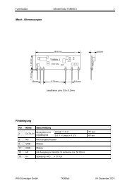
Transceiver module TRX433-10C2 / TRX868-10C2 (Vers. 1.0E) 5<br />
Dimensions<br />
0.5mm 24.5mm<br />
Pin description<br />
40.0mm<br />
TRX433-10<br />
TRX868-10<br />
front view<br />
14 13 12 11 10 9 8 7 6<br />
2 1<br />
2.54mm 10.16mm 2.54mm<br />
Lead frame: pins 0.5 x 0.2mm<br />
Pin Name I/O Description Level Condition<br />
4.5mm<br />
1 RF I/O RF- in/out for lambda / 4 antenna (~ 50 Ω) 0 V DC-path to GND<br />
2 GND RF Signal Ground<br />
6 V_P O Programming voltage (do not connect) VCC<br />
7 MCLR\ I Reset input, active low. 3 VCC Normal operation<br />
8 RSSI O Received Signal Strength Indicator (analog out) 0 V -128 dBm<br />
9 RTS O RTS handshake 0 V Ready to send<br />
10 TxD O UART transmit data (digital out) VCC Stop bit or no data<br />
11 RxD I UART receive data (digital in) VCC Stop bit or no data<br />
12<br />
CTS<br />
MODE<br />
WKUP<br />
I<br />
I<br />
I<br />
CTS handshake<br />
Interface mode (data or configuration)<br />
Sleep mode: Pin change terminates sleep<br />
13 V+ Positive supply voltage<br />
14 GND Ground<br />
0 V<br />
0 V<br />
Clear to send<br />
Data mode<br />
3.5 to 6VDC 4 or<br />
2.4 to 3.6VDC 5<br />
3<br />
connect an external reset controller, if supply voltage is not always within specified limits or if voltage<br />
ramp is slower than 50ms from 0V to 3.5V.<br />
4<br />
standard version with internal 3.3V supply voltage regulator (output logic high levels are limited to the<br />
internal 3.3V supply voltage)<br />
5<br />
version without internal voltage regulator (internal supply voltage = V+)
Transceiver module TRX433-10C2 / TRX868-10C2 (Vers. 1.0E) 6<br />
General information<br />
Serial Interface (RS232)<br />
There is a serial bidirectional full duplex interface available to communicate with the transceiver module. The<br />
data are transmitted and the transceiver module is configured over the same interface. You can choose<br />
between data mode and configuration mode with the MODE pin.<br />
Data mode (MODE Pin = Low)<br />
When the transceiver module receives data over the serial interface then those are automatically transmitted<br />
to all transceivers with the same configurations (frequency, RF data rate etc). Then those transceivers output<br />
them immediately over the serial interface after a few milliseconds. The baud rate for the RS232transmission<br />
can be set from 1.2kbaud to 115.2kbaud 6 .<br />
Configuration mode (MODE Pin = High)<br />
The transceiver module is configured over the serial interface. There is a comprehensive command set<br />
available. The last configuration will stay saved in the internal EEPROM if the accordant bit for saving in<br />
EEPROM is set. The configuration can occur in any baud rate from 1.2kbaud to 115.2kbaud 6 (the baud rate<br />
is detected automatically in the configuration mode).<br />
Radio transmission<br />
In the data mode, all the data which was received by the transceiver module over the serial interface are<br />
transmitted autonomous via radio. The transceiver module completely does the coding and decoding of the<br />
radio transmission. However, you can adjust the radio transmission to your own needs with help of a few<br />
simple commands. The following configurations can be done:<br />
Frequency selection<br />
There are 139 frequencies in 433MHz–band respectively 159 frequencies in 868MHz–band available, in<br />
each case in the 12.5 kHz–channel spacing. The frequency can be chosen irrespectively of the adjusted RF<br />
data rate. Make sure that on systems with several used frequencies, the frequency separation is at least the<br />
same as the occupied channels of the adjusted RF data rate (see table 1). This frequency separation has to<br />
be raised as high as possible for a better range.<br />
RF data rate<br />
The RF data rate can be chosen from 1.2kbits/s to 38.4kbits/s 7 according to requirements. The smaller the<br />
RF data rate is chosen, the higher is the radio range between the transceiver modules. RF data rates ><br />
19.2kbits/s are possible but they require an accordant dimensioned loop filter respectively a change in<br />
assembling. Through this change, the sensitivity of the receiver with low RF data rates is reduced. The basic<br />
model TRXnnn-10C2 is assembled with loop filters for max. 19.2kbits/s.<br />
Further radio transmission configurations to the chosen RF data rates are made automatically by the<br />
transceiver modules. These configurations for the different possible RF data rates can be found in table 1.<br />
RF data rates Coding Modulation FM-deviation IF-bandwidth Occupied<br />
channels<br />
1.2 kbit/s<br />
2.4 kbit/s<br />
4.8 kbit/s<br />
9.6 kbit/s<br />
19.2 kbit/s<br />
38.4 kbit/s 7<br />
Manchester GFSK<br />
Manchester GFSK<br />
NRZ GFSK<br />
NRZ GFSK<br />
NRZ GFSK<br />
NRZ GFSK<br />
NRZ GFSK<br />
NRZ GFSK<br />
+- 2.025 kHz<br />
+- 2.025 kHz<br />
+- 2.025 kHz<br />
+- 2.025 kHz<br />
+- 4.050 kHz<br />
+- 4.950 kHz<br />
+- 9.900 kHz<br />
+- 19.80 kHz<br />
9.6 kHz<br />
12.3 kHz<br />
9.6 kHz<br />
12.3 kHz<br />
19.2 kHz<br />
25.6 kHz<br />
51.2 kHz<br />
102.4 kHz<br />
1 x 12.5kHz<br />
1 x 12.5kHz<br />
1 x 12.5kHz<br />
1 x 12.5kHz<br />
2 x 12.5kHz<br />
4 x 12.5kHz<br />
8 x 12.5kHz<br />
12 x 12.5kHz<br />
Table 1 RF data rate with corresponding further configurations can be chosen.<br />
Comment<br />
433 MHz<br />
868 MHz<br />
433 MHz<br />
868 MHz<br />
6<br />
115.2kbaud requires a 16MHz µP clock frequency<br />
7<br />
RF data rate > 19.2kbits/s requires a modification of the loop filter, therefore a change in assembling and a<br />
16MHz µP clock frequency
Transceiver module TRX433-10C2 / TRX868-10C2 (Vers. 1.0E) 7<br />
Radio telegram structure<br />
For the radio transmission, the actual payloads are embedded in a radio telegram. The transceiver module<br />
builds the radio telegram and the associated coding and decoding and disburdens the user with that. A<br />
complete radio telegram is built according to figure 1.<br />
2ms Startup +<br />
Preamble<br />
Syncword<br />
2ms + 32 bits 24 bits 8 bits<br />
(opt.)<br />
Figure 1 structure of the radio telegram<br />
Functions of the individual blocks in the radio telegram<br />
LengthField<br />
DataField<br />
CRC16<br />
n x 8/9 bits (depends on fastsend-setting) 16 bits<br />
(opt.)<br />
2ms startup: settling time for the transmitter for the reduction of the transient emissions<br />
Preamble: allows the receiver to level out to the carrier signal of the transmitter<br />
Syncword: indiales start of the data transmission and conduces therefore to the receiver to synchronize<br />
LenthField: declares number of bytes payload in the DataField (optional)<br />
DataField: effective payload<br />
CDC16: checksum for payload in the data field (optional)<br />
Postamble: sends for the correct receiving of the last Data bits of the radio telegram<br />
Every radio telegram has to consist of 2ms Startup + Preamble, Syncword, DataField and Postamble. The<br />
blocks LengthField and CRC16 are, depending on the chosen configuration, added to the radio telegram as<br />
well. The duration of the individual blocks depends on the adjusted RF data rate and is calculated out of the<br />
number of bits multiplied by the bit duration of the adjusted RF data rate. Only the period of the 2ms Startup<br />
stays constantly 2ms with every RF data rate.<br />
Transmittion- and receiving buffer<br />
The transceiver module has a transmittion - and receiving buffer, 61 bytes each, for the serial interface.<br />
Transmittion buffer (TX-BUF)<br />
Over RS232 received data are buffered in the transmittion buffer. The space in the transmittion buffer frees<br />
byte-by-byte as soon as a byte is inserted into its place in the DataField of the radio telegramm.<br />
Receiving buffer (RX-BUF)<br />
In the receiving buffer, the over radio received data are buffered until their output over RS232. When the<br />
function “Output of the telegram-RSSI” respectively “Output of the no signal condition-RSSI” is enabled then<br />
these RSSI-values are buffered in the receiving buffer in addition to the payloads of the radio telegram.<br />
Depending on the configuration, there are maximum two additional bytes needed in the receiving buffer per<br />
radio telegram. The space in the receiving buffer for the receiving of the radio telegram has to be free by the<br />
time the radio telegram receives the actual payloads from the DataField. The space in the receiving buffer is<br />
freed byte-by-byte as soon as a byte is output over RS232.<br />
Postamble<br />
2 bits
Transceiver module TRX433-10C2 / TRX868-10C2 (Vers. 1.0E) 8<br />
Buffer overflow<br />
Be careful that the two buffers (transmittion- and receiving buffer) don’t overflow. That can be ensured by<br />
adhere the right timing or by using the handshake (see paragraph Example of data flow and Handshake with<br />
RTS/CTS).<br />
Overflow of the transmittion buffer<br />
The transmittion buffer has, additionally to its 61 bytes, a 2-byte overflow buffer. So when the transmittion<br />
buffer is full (61 bytes full) and further data are still transferred over RS232 then max. 2 bytes can be saved<br />
in the overflow buffer. Those will be transferred in the transmittion buffer as soon as there is space in there.<br />
When the overflow buffer is full as well then further over the RS232 received data will be rejected.<br />
Overflow of the receive buffer<br />
The receiving buffer has, additionally to its 61 bytes, a 2-byte overflow buffer. This buffer is only used for<br />
saving the RSSI-values in addition to the payload if the function “Output of the telegram-RSSI” respectively<br />
“output of the no signal condition-RSSI” is enabled and if the whole 61 bytes of the receiving buffer are full<br />
with the radio telegram.<br />
When data are received over radio even if the buffer is already full (61 bytes full), then the whole incoming<br />
radio telegram will be rejected if the CRC16 is on. If the CRC16 is off then the already received data will be<br />
saved and the rest of the incoming radio telegram will be rejected.<br />
Handshake with RTS/CTS<br />
The communication over the RS232-interface can be controlled with help of RTS/CTS to avoid overflowing of<br />
buffers. RTS and CTS are only used for the handshake when the handshake is activated. When the<br />
handshake is disabled then the RTS and CTS are ignored.<br />
Function RTS<br />
As soon as 61 bytes are saved in the transmittion buffer then the transceiver module stops the receiving of<br />
data over RS232 by setting the RTS-Pin on high. The user may not send further data over the RS232interface<br />
to the transceiver module until the RTS-pin changes to low again. The RS232-interface enables<br />
again (RTS-Pin reset to low) once ≤58 bytes are saved in the transmittion buffer.<br />
Function CTS<br />
With an activated handshake, the user can stop the output of data of the transceiver module by setting the<br />
CTS-Pin to high. The transceiver module doesn’t output any more data over the TxD-Pin until the CTS-Pin is<br />
set back to low by the user.<br />
Note<br />
If the CTS-Pin is used as handshake, don’t send any data to the transceiver module during the high-time of<br />
the CTS-Pin because these data would be interpreted as configuration data. The CTS-Pin has the double<br />
function handshake (CTS) and interface mode (MODE).<br />
Figure 2 shows the cycle of a data communication of 64 bytes with use of the handshake. There, module 1 is<br />
the transceiver and module 2 is the receiver. Additionally you can see how many bytes are saved in the<br />
transmittion buffer (TX-BUF) of the sending transceiver module and in the receiving buffer (RX-BUF) of the<br />
receiving transceiver module.<br />
module 1<br />
module 2<br />
bytes in TX-BUF ... 0........... 1........... ........60......... 61................................................................60.59.58.57.56. 56.55.55.54.53. 53.... ....3......................................................... 2...1...0..................................... ...............<br />
RS232, RTS-pin<br />
RS232, RxD-pin<br />
RF-transmission<br />
RS232, TxD-pin<br />
Byte 1<br />
Byte 2<br />
Byte 60<br />
Byte 61<br />
start RF-transmission<br />
after 2-3 bytes break<br />
32 Bit<br />
Preamble<br />
+2ms<br />
Startup<br />
24 Bit<br />
SYNC<br />
Byte 62<br />
Length<br />
Byte 1<br />
Byte 2<br />
Byte 3<br />
Byte 4<br />
Byte 5<br />
Byte 6<br />
Byte 7<br />
Byte 8<br />
Byte 9<br />
Byte 10<br />
Byte 11<br />
Byte 63<br />
Byte 64<br />
Byte 60<br />
Byte 61<br />
CRC16<br />
32 Bit<br />
Preamble<br />
+2ms<br />
Startup<br />
Byte 1<br />
Byte 2<br />
24 Bit<br />
SYNC<br />
Byte 3<br />
Length<br />
Byte 62<br />
Byte 63<br />
Byte 64<br />
bytes in RX-BUF ... 0......................... ........................................................................................................................................................... .................. 61.........60.........59.........58.........57.........56. 59... 58.......... .........0....<br />
Figure 2 data communication with handshake<br />
start RF-transmission<br />
after 2-3 bytes break<br />
Byte 4<br />
Byte 5<br />
CRC16<br />
Byte 6<br />
Byte 7<br />
Byte 64
Transceiver module TRX433-10C2 / TRX868-10C2 (Vers. 1.0E) 9<br />
CRC16<br />
The CRC16 is a 16-Bit check sum which checks the payloads in the DataField for correctnes. If the higher<br />
application doesn’t check the data then you should definitely use the CRC16.<br />
CRC16 off<br />
The radio data are not checked for correctness. The RS232 receives a data byte from the DataField of the<br />
radio telegram and outputs it immediately. The higher application has to deal with the checking of the data.<br />
CRC16 on<br />
The payloads in the DataField are CRC16-checksum-verified and the calculated checksum is included on<br />
the end of the radio telegram. That means that the data of the receiving transceiver module will only be<br />
output over RS232 when CRC16 corresponds. By wrong CRC16, the whole radio telegram will be rejected.<br />
Fast send<br />
The configuration Fast send decides when the radio transmission of the over the RS232 received payloads<br />
starts and in which way the radio telegram length is transmitted.<br />
Fast send off<br />
The data which were received in one piece over the RS232 are buffered in the transmittion buffer. As soon<br />
as no further data is received over the RS232 for the time of 2-3 RS232-bytes then the radio transmission<br />
starts and the current stored payloads in the transmittion buffer are transmitted. The length of the radio<br />
telegram is therefore defined at the beginning of the radio transmission (in the LengthField, the number of<br />
bytes of payloads are entered). When further data are received over RS232 during the radio transmission,<br />
they will be buffered in the transmittion buffer and they’ll build a new radio telegram as soon as the radio<br />
transmission of the current radio telegram is complete.<br />
Fast send on<br />
The radio transmission starts once the first byte is received over RS232 and will not stop until no byte is left<br />
in the transmittion buffer. Therefore the length of a radio telegram is not known in the beginning of the radio<br />
transmission. That’s why no LengthField is added to the radio telegram. To label the radio telegram length, a<br />
bit is added to every payload byte in the DataField which shows the end of the payloads.<br />
Note<br />
• Although the radio transmission starts earlier with Fast send than without, one bit is added to every<br />
payload byte in the DataField for the identification of the radio telegram length. Thereby, a radio telegram<br />
with fast send on and more than 8 bytes payload gets longer than one without fast send.<br />
• Due to the fact that Fast send means more computing effort, Fast send can only be used up to a RF data<br />
rate of 19.2kbits/s (respectively 9.6kbits/s by 8MHz µP clock frequency).<br />
• The radio telegram length is limited to 61 bytes with Fast send when CRC16 is enabled because the<br />
receiver has to buffer the whole radio telegram until CRC16 is checked. The user has to make sure that<br />
the length of the radio telegram is no more than 61 bytes payload.<br />
• With disabled CRC16 and Fast send on, a radio telegram length with over 61 bytes payload is possible.<br />
• The pause with the period of 2-3 RS232-bytes for the start of the radio transmission without Fast send<br />
varies depending on the adjusted configuration. To make sure that the radio transmission really will start<br />
you should keep a minimum pause of three RS232-bytes.
Transceiver module TRX433-10C2 / TRX868-10C2 (Vers. 1.0E) 10<br />
Examples of data flow<br />
Following, there are some examples by which you can see the data flow by different configuration of Fast<br />
send, CRC16, Handshake etc.<br />
Examples for different configuration of fast send and CRC16<br />
Refer to the figure for the data flow which depends on the configuration of Fast send and CRC16. Thereby,<br />
module 1 is used as transceiver and module 2 is used as receiver. Of course several modules with the same<br />
configuration as the transceiver can receive the data signal.<br />
module 1<br />
module 2<br />
RS232, RxD-pin<br />
RF-transmission<br />
RS232, TxD-pin<br />
Byte 1<br />
Byte 2<br />
Byte 3<br />
Byte 4<br />
start RF-transmission<br />
after 2-3 bytes break<br />
32 Bit<br />
Preamble<br />
+2ms<br />
Startup<br />
24 Bit<br />
SYNC<br />
Length<br />
Byte 1<br />
Byte 2<br />
Byte 3<br />
Byte 4<br />
CRC16<br />
Figure 3 Dataflow without Fast send with CRC16, RF data rate > RS232-baud rate<br />
module 1<br />
module 2<br />
RS232, RxD-pin<br />
RF-transmission<br />
RS232, TxD-pin<br />
Byte 1<br />
Byte 2<br />
Byte 3<br />
Byte 4<br />
start RF-transmission<br />
after 2-3 bytes break<br />
32 Bit<br />
Preamble<br />
+2ms<br />
Startup<br />
24 Bit<br />
SYNC<br />
Length<br />
Byte 1<br />
Byte 2<br />
Byte 3<br />
Byte 4<br />
Byte 1<br />
Byte 2<br />
Byte 1<br />
Byte 3<br />
output after first<br />
received databyte<br />
Figure 4 Dataflow without Fast send without CRC16, RF data rate > RS232-baud rate<br />
module 1<br />
module 2<br />
RS232, RxD-pin<br />
RF-transmission<br />
RS232, TxD-pin<br />
Byte 1<br />
Byte 2<br />
Byte 3<br />
Byte 4<br />
start RF-transmission<br />
after 2-3 bytes break<br />
2<br />
32 Bit<br />
Byte<br />
Preamble<br />
24 Bit<br />
+2ms Startup<br />
SYNC<br />
Figure 5 Dataflow without Fast send without CRC16, RF data rate < RS232-baud rate<br />
Length<br />
Byte 1<br />
Byte 1<br />
Byte 2<br />
Byte 3<br />
Byte 3<br />
Byte 4<br />
Byte 4<br />
output after first<br />
received databyte<br />
Byte 2<br />
Byte 3<br />
output after<br />
checked CRC16<br />
Byte 4<br />
Byte 4
Transceiver module TRX433-10C2 / TRX868-10C2 (Vers. 1.0E) 11<br />
module 1<br />
module 2<br />
RS232, RxD-pin<br />
RF-transmission<br />
RS232, TxD-pin<br />
Byte 1<br />
Byte 2<br />
32 Bit<br />
Preamble<br />
+2ms<br />
Startup<br />
Byte 3<br />
24 Bit<br />
SYNC<br />
Byte 4<br />
Byte 1<br />
Byte 2<br />
Byte 3<br />
Byte 4<br />
start RF-transmission after<br />
first received RS232-byte<br />
CRC16<br />
Byte 1<br />
Byte 2<br />
Byte 3<br />
output after<br />
checked CRC16<br />
Figure 6 Dataflow with Fast send with CRC16, RF data rate > RS232-baud rate<br />
module 1<br />
module 2<br />
RS232, RxD-pin<br />
RF-transmission<br />
RS232, TxD-pin<br />
Byte 1<br />
Byte 2<br />
32 Bit<br />
Preamble<br />
+2ms<br />
Startup<br />
Byte 3<br />
24 Bit<br />
SYNC<br />
Byte 4<br />
Byte 1<br />
Byte 2<br />
Byte 3<br />
Byte 4<br />
start RF-transmission<br />
after first received RS232-byte<br />
Byte 1<br />
Byte 2<br />
Byte 3<br />
output after first<br />
received databyte<br />
Figure 7 Dataflow with Fast send without CRC16, RF data rate > RS232-baud rate<br />
module 1<br />
module 2<br />
RS232, RxD-pin<br />
RF-transmission<br />
RS232, TxD-pin<br />
Byte 1<br />
Byte 2<br />
Byte 3<br />
Byte 4<br />
2<br />
32 Bit<br />
Byte<br />
Preamble<br />
24 Bit<br />
+2ms Startup<br />
SYNC<br />
start RF-transmission after<br />
first received RS232-byte<br />
Byte 1<br />
Byte 1<br />
Byte 4<br />
Byte 2<br />
Byte 3<br />
Byte 3<br />
Byte 4<br />
output after first<br />
received databyte<br />
Figure 8 Dataflow with Fast send without CRC16, RF data rate < RS232-baud rate<br />
Byte 4<br />
Byte 4
Transceiver module TRX433-10C2 / TRX868-10C2 (Vers. 1.0E) 12<br />
Example for a continued radio data stream (radio telegram with more than 61 bytes payload)<br />
A continued radio data stream (thus a telegram which isn’t limited to 61 bytes payload) can only be realized<br />
with Fast send and without CRC16. Also, the RS232-baud rate has to be chosen at least as fast as the RF<br />
data rate. With these configurations, a continued radio data stream like in figure 9 can be realized. It is also<br />
apparent in Figure 9 how the CTS pin may prevent the transceiver module from outputting the data via<br />
RS232 that it received via radio. Also you can see the number of bytes in the transmittion buffer (TX-BUF) of<br />
the sending transceiver module and the numbers of bytes in the receiving buffer (RX-BUR) of the receiving<br />
transceiver module.<br />
module 1<br />
module 2<br />
bytes in TX-BUF<br />
RS232, RTS-pin<br />
RS232, RxD-pin<br />
RF-transmission<br />
RS232, TxD-pin<br />
RS232, CTS-pin<br />
bytes in RX-BUF<br />
0.... 1.... 2.... 3.... 4.... 5.... 6.... 7.... 8.... 9....10...11...12...12...12...13...13...14...14...15...15...<br />
Byte 1<br />
Byte 2<br />
Byte 3<br />
Byte 4<br />
32 Bit<br />
Preamble<br />
+2ms Startup<br />
Byte 5<br />
Byte 6<br />
Byte 7<br />
Byte 8<br />
Byte 9<br />
Byte 10<br />
24 Bit<br />
SYNC<br />
Byte 11<br />
Byte 12<br />
Byte 13<br />
Byte 1<br />
Byte 14<br />
Byte 15<br />
Byte 2<br />
Byte 16<br />
Byte 17<br />
Byte 3<br />
Byte 18<br />
Byte 19<br />
Byte 4<br />
Byte 20<br />
... 0........................................................................................ 1....0....1....0.... 1....0....1....0... ....0....1....0....1....0....1..........2..........3...2.....2....1...2.1...0..1....0....1....0....1....0..<br />
Figure 9 Dataflow with Fast send without CRC16, RS232-baud rate = 2x RF data rate<br />
Byte 5<br />
Byte 21<br />
Byte 121<br />
60...60...61. 60........59........ 58...59...59...60...60...61.60.... 59........58... 59...59...<br />
Example for continued data stream over RS232<br />
With Fast send enabled and CRC16 disabled, a continued data stream can be realized over the RS232interface.<br />
For that, the RF data rate has to be chosen higher than the RS232-baud rate. In figure 10, a<br />
continued data stream over RS232 is shown by which the RF data rate is adjusted twice as fast as the<br />
RS232-baud rate. Further you can see how many bytes are stored in the transmittion buffer (TX-BUF) of the<br />
sending transceiver module and in the receiving buffer (RX-BUF) of the receiving transceiver module.<br />
module 1<br />
module 2<br />
bytes in TX-BUF<br />
RS232, RTS-pin<br />
RS232, RxD-pin<br />
RF-transmission<br />
RS232, TxD-pin<br />
RS232, CTS-pin<br />
bytes in RX-BUF<br />
Byte 1<br />
Byte 2<br />
Byte 3<br />
Byte 4<br />
...0........... 1...........2...........3........ 2. . 3. 2...1..2.1...0....1...........2...........3......... 2.3..2....1.2...1...0..1...........2...........3..........4.3...2.... 2...1...0.1...........2...........3...........4..3...2..3. 2...<br />
Byte 1<br />
Byte 2<br />
32 Bit<br />
Preamble<br />
+2ms<br />
Startup<br />
Byte 3<br />
24 Bit<br />
SYNC<br />
Byte 4<br />
Byte 1<br />
Byte 5<br />
Byte 2<br />
Byte 3<br />
Byte 4<br />
Byte 5<br />
Byte 1<br />
Byte 6<br />
Byte 7<br />
Byte Byte 1 8<br />
32 Bit<br />
Preamble<br />
+2ms<br />
Startup<br />
Byte Byte 1 9<br />
24 Bit<br />
SYNC<br />
Byte Byte 1 10<br />
...0....................................................... 1... 2...3.2..3...4..3.......... 2...........1.......... 0.1...2...3.2..3...4..3.......... 2...........1..........0.1...2...3.2..3...4..3.......... 2...........1...........0.1.... 2...<br />
Byte 60<br />
Byte Byte 1 11<br />
Byte 6<br />
Byte 7<br />
Byte 8<br />
Byte 9<br />
Byte 10<br />
Byte 61<br />
Byte 122<br />
Byte 123<br />
Byte 61<br />
Byte Byte 1 12<br />
Byte 62<br />
Byte 62<br />
Byte 63<br />
Byte Byte 1 13<br />
32 Bit<br />
Preamble<br />
+2ms<br />
Startup<br />
Byte 64<br />
Byte Byte 1 14<br />
24 Bit<br />
SYNC<br />
Byte 124<br />
Byte 65<br />
Byte Byte 1 15<br />
Byte 125<br />
Byte 63<br />
Byte 126<br />
Byte 66<br />
Byte 64<br />
Byte 127<br />
Byte Byte 1 16<br />
Byte 11<br />
Byte 12<br />
Byte 13<br />
Byte 14<br />
Byte 15<br />
Figure 10 Data stream with Fast send without CRC16, RF data rate = 2x RS232-baud rate<br />
Byte 2<br />
Byte 3<br />
Byte 4<br />
Byte 5<br />
Byte 6<br />
Byte 7<br />
Byte Byte 1 8<br />
Byte Byte 1 9<br />
Byte Byte 1 10<br />
Byte Byte 1 11<br />
Byte 65<br />
Byte 128<br />
Byte 67<br />
Byte Byte 1 12<br />
Byte 66<br />
Byte Byte 1 17<br />
Byte 67<br />
Byte 68<br />
Byte Byte 1 18<br />
32 Bit<br />
Preamble<br />
+2ms<br />
Startup<br />
Byte Byte 1 13<br />
Byte 68<br />
Byte 69<br />
Byte Byte 1 14<br />
Byte 129<br />
Byte 69<br />
Byte Byte 1 19<br />
Byte 70<br />
24 Bit<br />
SYNC<br />
Byte 130<br />
Byte Byte 1 15<br />
Byte 70<br />
Byte Byte 1 20<br />
Byte 16<br />
Byte 71<br />
Byte 17<br />
Byte 131 60<br />
Byte 16<br />
Byte 21<br />
Byte 18
Transceiver module TRX433-10C2 / TRX868-10C2 (Vers. 1.0E) 13<br />
RSSI of the telegram and no signal condition-RSSI<br />
To define the quality of a radio connection, the received sighnal strength indicator (RSSI) of the just received<br />
radio telegram can be output over RS232 after every received radio telegram. The signal strength will be<br />
output in dBm in addition to the payloads of the radio telegram in a twos complement.<br />
The no signal condition - RSSI can be output optionally in addition to the RSSI of the telegram. The RSSIvalue<br />
which was measured immediately after the radio telegram will be output as a no signal condition -<br />
RSSI. Out of those two RSSI-values, the signal-noise ratio can be calculated. Of course, the no signal<br />
condition-RSSI can be read out with the command “READ RSSI current” as well. You can see the output of<br />
the telegram-RSSI (RSSI TLG) and of the no signal condition-RSSI (RSSI at no signal condition) added to<br />
the payload in figure 11.<br />
Note<br />
When the function “Output of the telegram-RSSI” respectively “Output of the no signal condition - RSSI” is<br />
enabled, then those RSSI-values are buffered in the receive buffer of the transceiver following the payload<br />
until they are output over RS232. Depending on the configuration, maximum 2 additional bytes are needed in<br />
the receive buffer per radio telegram.<br />
module 1<br />
module 2<br />
RS232, RxD-pin<br />
RF-transmission<br />
RS232, TxD-pin<br />
Byte 1<br />
Byte 2<br />
Byte 3<br />
Byte 4<br />
start RF-transmission<br />
after 2-3 bytes break<br />
32 Bit<br />
Preamble<br />
+2ms<br />
Startup<br />
24 Bit<br />
SYNC<br />
Length<br />
Byte 1<br />
Byte 2<br />
Byte 3<br />
Byte 4<br />
Figure 11 Output of the telegram-RSSI and the no signal condition-RSSI<br />
CRC16<br />
Byte 1<br />
Byte 2<br />
Byte 3<br />
output after<br />
checked CRC16<br />
Byte 4<br />
RSSI TLG<br />
RSSI Ruhe
Transceiver module TRX433-10C2 / TRX868-10C2 (Vers. 1.0E) 14<br />
Recalibration<br />
The VCO has to be recalibrated by a temperature variation of >40°C or by a variation of the supply voltage of<br />
> 0.25 volt (for version without voltage regulator). It can be calibrated automatically in defined intervals from<br />
5 to 150min, by temperature differences of more than 20°C or just once manual during the calibration<br />
command. During the calibration, which normally takes 50ms, no radio communicationl is possible.<br />
Beginning, end and result will be reported if the module is in the configuration mode.<br />
There occurs an automatic calibration with every power up. The last calibration stays stored in the RAM<br />
during the sleep. Therefore the transceiver is ready again pretty fast after the wakeup (by 19.2kbits/s RF<br />
data rate after 3ms, by 2.4kbits/s RF data rate after 5ms). When the temperatures or the supply voltage can<br />
change significantly during the sleep then you first have to recalibrate after the wake up.<br />
Energy-saving mode and characteristics by reset, power up, wake up und sleep<br />
The RF-part of the transceiver can be enabled and disabled with the command Power-control, as well as<br />
the LED. Disabled, the current consumption is highly reduced but the processor still stays active and uses<br />
electricity.<br />
The sleep command is for battery operated units which are mostly inactive and which may just use electricity<br />
during the radio communication. Thereby the current consumption can be reduced down to 3µA (version<br />
without intern voltage regulator) during the sleep. The version with voltage regulator uses ca. 100µA while<br />
sleeping. During the sleep, the transceiver is inactive but all the configurations and the last calibration remain<br />
in the RAM.<br />
High reserve energy is achievable due to the low current consumption during the sleep and the short setuptime<br />
after a wakeup of 3ms by 19.2kbits/s RF data rate respectively 5ms by 2.4kbits/s RF data rate because<br />
the average of the current consumption depends almost only on the proportion transmitting time/transmitting<br />
interval.<br />
The sleep command disables the RF-part and the LED and stops afterwards the clock of the micro controller.<br />
The behavior during the sleep as well as the behavior after a wakeup can be defined with the command<br />
parameter WKUP_mode of the sleep command. The timer for automatic recalibration is paused during the<br />
sleep.<br />
The WKUP-Pin has to be on its sleep-level (high or low) before the sleep but at the latest 50µs after the<br />
answer to the sleep command. Afterwards, the change in level automatically activates an immediate<br />
wakeup.<br />
The command power up mode is similar to the sleep command. The sleep command is performed<br />
immediately, the command power up mode doesn’t affects until the next power up. The transceiver can be<br />
configured with PWUP_mode so that it automatically changes to the sleep mode after the power up until it’s<br />
awoken and reconfigured from outside. This is important in battery operations so that the radio module<br />
doesn’t get active autonomously after a battery change and discharges the battery unnoticed.<br />
The sleep mode finishes through a pinchange on the WKUP-Pin. Thereby, the program either continues<br />
where it was interrupted by the sleep-command or there is an internal reset whereat a complete re-start<br />
occurs. When the transceiver is in the configuration mode (MODE-Pin = High) then it shows by “REPORT<br />
READY” on the RS232 that the microcontroller on the transceiver is ready. Alternatively, the RTS-Pin can be<br />
supervised. The RTS-Pin goes back to high after the sleep-command. The RTS-Pin is set back to low as<br />
soon as the transceiver is ready again after a wakeup (see figure 12 and 13).
Transceiver module TRX433-10C2 / TRX868-10C2 (Vers. 1.0E) 15<br />
RTS-pin<br />
MODE-pin and<br />
WKUP-pin resp.<br />
RS232, RxD-pin<br />
RS232, TxD-pin<br />
0B0H<br />
020H<br />
sleepcommand<br />
change to<br />
config-mode<br />
021H<br />
answer<br />
(only sent if still<br />
in config-mode)<br />
020H<br />
021H<br />
enter sleep<br />
030H<br />
wakeup (pinchange<br />
on WKUP-pin)<br />
max. 50us for pinchange, otherwise interpreted as wakeup<br />
001H<br />
ready after wakeup<br />
(only sent in config-mode)<br />
ready after wakeup<br />
Figure 12 Sleep and wake up with configuration mode after wake up<br />
RTS-pin<br />
MODE-pin and<br />
WKUP-pin resp.<br />
RS232, RxD-pin<br />
RS232, TxD-pin<br />
0B0H<br />
020H<br />
sleepcommand<br />
change to<br />
config-mode<br />
021H<br />
answer<br />
(only sent if still<br />
in config-mode)<br />
020H<br />
021H<br />
enter sleep<br />
030H<br />
wakeup (pinchange<br />
on WKUP-pin)<br />
Figure 13 Sleep and wakeup with data mode after wake up<br />
001H<br />
ready after wakeup<br />
ready after wakeup<br />
(suppressed because in data-mode)<br />
The transceiver module will report after ca. 175ms with a ready signal over RS232 after a power up if the<br />
transceiver module is in the configuration mode. A negative edge on the RTS-Pin can be used alternatively<br />
to it as a ready signal (see figure 14 respectively figure 15).<br />
VCC<br />
RTS-pin<br />
MODE-pin<br />
RS232, TxD-pin<br />
VCC on<br />
change to config-mode<br />
030H<br />
000H<br />
ready ca. 175ms<br />
after powerup<br />
ready ca. 175ms after powerup<br />
(only sent in config-mode)<br />
Figure 14 Powerup with transceiver module in configuration mode
Transceiver module TRX433-10C2 / TRX868-10C2 (Vers. 1.0E) 16<br />
VCC<br />
RTS-pin<br />
MODE-pin<br />
RS232, TxD-pin<br />
VCC on<br />
stay in data-mode<br />
Figure 15 Powerup with transceivermodul in data mode<br />
030H<br />
000H<br />
ready ca. 175ms<br />
after powerup<br />
ready ca. 175ms after powerup<br />
(suppressed because in data-mode)<br />
Note<br />
• Pay attention to the paragraph supply voltage and MCLR/Reset whenever the supply switches!<br />
• The most capacity of battery can generally be saved with the sleep-function. We recommend using the<br />
sleep-function instead of switching the supply.
Transceiver module TRX433-10C2 / TRX868-10C2 (Vers. 1.0E) 17<br />
RSSI (Received Signal Strength Indicator)<br />
There is a voltage on pin 8 (RSSI) which is directly proportional to the RF - field strength. The transceiver<br />
scans the field strength every 3ms and outputs the RSSI-value as analogue voltage to pin 8.<br />
The voltage on the RSSI-pin follows this equation:<br />
Urssi<br />
1.5 * 3.3V<br />
PRF [dBm] = − 128 + * 127<br />
Zero-point by -128 dBm, Slope: 25.7dB/V, Measurement range -120…-60 dBm<br />
The RSSI-pin shows an internal resistance of ca. 10kΩ<br />
RSSI characteristic<br />
-140 -130 -120 -110 -100 -90 -80 -70 -60 -50 -40 -30 -20 -10 0<br />
Phf [dBm]<br />
Figure 16 Tension on RSSI-pin<br />
PRF can be read out digitally as a RSSI value with the command “READ RSSI current”, whereat the value is<br />
output directly in the twos complement in the unit dBm<br />
Examples: PRF = -128 dBm makes a RSSI of 128dec respectively 080H (under the noise floor)<br />
PRF = -120 dBm makes a RSSI of 136dec respectively 088H<br />
PRF = -110 dBm makes a RSSI of 146dec respectively 092H<br />
PRF = -100 dBm makes a RSSI of 156dec respectively 09CH<br />
PRF = -60 dBm makes a RSSI of 196dec respectively 0C4H (saturation limit)<br />
The maximal value of the RSSI will be saved by the transceiver (peak hold) and can be read out as well with<br />
the command “READ RSSI peak” as well. Every read operation of the RSSI peak initializes thereby the<br />
maximal value so that the maximal value represents the period between two read operations. The RSSI<br />
peak is initialized right after a sleep as well.<br />
The RSSI current and the RSSI peak go back to -128dBm during transmission<br />
3.50<br />
3.00<br />
2.50<br />
2.00<br />
1.50<br />
1.00<br />
0.50<br />
0.00
Transceiver module TRX433-10C2 / TRX868-10C2 (Vers. 1.0E) 18<br />
Power supply<br />
The radio transceiver with the voltage regulator needs a good supply voltage with minimum 3.5V and a ripple<br />
of < 10mVpp. The power amplifier is directly located on the input side of the supply voltage. The<br />
transmission power is therefore to a minor degree dependant on supply voltage. When the supply is<br />
switched then the voltage has to fall back to 0V after disabling it before you can enable it again. The supply<br />
voltage has to rise from 0V to 3.5V during max 50ms so that the integrated microcontroller starts correctly.<br />
The voltage can never fall under 3.3 Volt, not even momentary. If this can’t be guaranteed then the supply<br />
has to be supervised with a voltage detector. As soon as it falls under ca. 3.3V, the input MCLR\ has to be<br />
pulled down. See application example with Demokit3.<br />
The radio transceiver without voltage regulator can operate from 2.4V to 3.6V. Keep a ripple of 3.3Volt (for standard TRX with 3.3V<br />
internal voltage regulator). The trip voltage can be reduced down to 2.3V by versions without a voltage<br />
regulator and a reduced µP clock frequency.<br />
When you follow the under the paragraph Power supply listed points then there is no external voltage<br />
detector necessary.<br />
After a reset on MCLR\Reset input, the transceiver normally needs 75ms to the output of the ready signal<br />
because the transceiver is calibrated and configured automatically after a reset. The ready signal will only be<br />
output if the module is in the configuration mode.<br />
Status LED<br />
The status of the transceiver-LED is defined by the command power-control. When that command<br />
accomplished with a set Bit7 then the LED will enable or disable by a powerup accordingly.<br />
After a sleep-command the LED is always turned off and after the wakeup the LED is always set back to the<br />
status it had before the sleep.
Transceiver module TRX433-10C2 / TRX868-10C2 (Vers. 1.0E) 19<br />
Temperature sensor<br />
The transceiver module has an internal temperature sensor. The current temperature can be read by the<br />
command “READ temperature”. The value range is in between -40°C to +115°C. The temperature is<br />
actualized every 5s, no matter how often it is read.<br />
Note<br />
The 5s-timer for the actualization of the temperature is stopped during the sleep. After the sleep, the<br />
temperature which was read before the sleep can therefore be displayed for 5s. This temperature can differ<br />
from the current temperature by a long sleep-time.
Transceiver module TRX433-10C2 / TRX868-10C2 (Vers. 1.0E) 20<br />
Technical data TRX433-10C<br />
Frequency range 433.0625.... 434.7875 MHz (12.5 kHz channel spacing)<br />
RF data rate<br />
Possible parameterization<br />
of the RF data rate with the<br />
corresponding fixed<br />
configuration.<br />
Coding Occupied<br />
channel<br />
IF-bandwidth FM-Deviation<br />
(Standard version up to<br />
19.2kbits/s 8 1.2 kbit/s<br />
2.4 kbit/s<br />
4.8 kbit/s<br />
)<br />
9.6 kbit/s<br />
19.2 kbit/s<br />
38.4 kbit/s 8<br />
Manchester 1 x 12.5 kHz<br />
NRZ 1 x 12.5 kHz<br />
NRZ 2 x 12.5 kHz<br />
9.6 kHz<br />
9.6 kHz<br />
19.2 kHz<br />
+- 2.025 kHz<br />
+- 2.025 kHz<br />
+- 4.050 kHz<br />
NRZ<br />
NRZ<br />
NRZ<br />
4 x 12.5 kHz<br />
8 x 12.5 kHz<br />
12 x 12.5 kHz<br />
25.6 kHz<br />
51.2 kHz<br />
102.4 kHz<br />
+- 4.950 kHz<br />
+- 9.900 kHz<br />
+- 19.80 kHz<br />
-120 dBm with RF data rate = 1.2kbit/s<br />
Receiver sensitivity by<br />
different parameterization<br />
(50 Ohm / BER = 1E-3)<br />
-118 dBm<br />
-115 dBm<br />
-113 dBm<br />
-110 dBm<br />
-106 dBm<br />
with RF data rate = 2.4kbit/s<br />
with RF data rate = 4.8kbit/s<br />
with RF data rate = 9.6kbit/s<br />
with RF data rate = 19.2kbit/s<br />
with RF data rate = 38.4kbit/s 8<br />
Frequency tolerance<br />
± 5ppm standard (Temp. -10°C ... +60°C)<br />
± 2ppm optional (Temp. -10°C ... +60°C)<br />
Transmission power<br />
+12 dBm, supply 5.0 V<br />
+10 dBm, supply 3.5 V<br />
Modulation GFSK<br />
Radio range by<br />
free sight 9<br />
2000m with RF data rate = 1.2kbit/s<br />
efficient instruction set<br />
supports functions like:<br />
Power-control, defines behavior by Power up, sleep, standby<br />
calibration, RSSI-output, read module temperature, read and write register,<br />
direct EEPROM-access (read, write),<br />
Serial number, Hardware, Software version etc.<br />
serial over RS232 with TTL level, 8 Data bits, 1 Stop bit, no parity<br />
baud rates: 1.2 / 2.4 / 4.8 / 9.6 / 19.2 / 38.4 / 57.6 / 115.2<br />
Data interface<br />
10 kbaud<br />
automatic baud rate detection on configuration<br />
Handshake with RTS/CTS<br />
61 bytes transmittion buffer and receive buffer<br />
supply<br />
3.5 to 6 V DC not stabilized, Ripple
Transceiver module TRX433-10C2 / TRX868-10C2 (Vers. 1.0E) 21<br />
Technical data TRX868-10C<br />
Frequency range 868.0125.... 869.9875 MHz (12.5 kHz channel spacing)<br />
RF data rate<br />
Possible parameterization<br />
of the RF data rate with the<br />
corresponding fixed<br />
configuration<br />
coding Occupied<br />
channels<br />
IF-bandwidth FM-Deviation<br />
(Standard version up to<br />
19.2kbits/s 11 1.2 kbit/s<br />
2.4 kbit/s<br />
4.8 kbit/s<br />
)<br />
9.6 kbit/s<br />
19.2 kbit/s<br />
38.4 kbit/s 11<br />
Manchester 1 x 12.5 kHz<br />
NRZ 1 x 12.5 kHz<br />
NRZ 2 x 12.5 kHz<br />
9.6 kHz<br />
9.6 kHz<br />
19.2 kHz<br />
+- 2.025 kHz<br />
+- 2.025 kHz<br />
+- 4.050 kHz<br />
NRZ<br />
NRZ<br />
NRZ<br />
4 x 12.5 kHz<br />
8 x 12.5 kHz<br />
12 x 12.5 kHz<br />
25.6 kHz<br />
51.2 kHz<br />
102.4 kHz<br />
+- 4.950 kHz<br />
+- 9.900 kHz<br />
+- 19.80 kHz<br />
Receiver sensitivity(50 Ohm -115 dBm<br />
/ BER = 1E-3)<br />
With RF data rate= 1.2kbit/s<br />
Frequency tolerancee<br />
± 5ppm standard (Temp. -10°C ... +60°C)<br />
± 2ppm optional (Temp. -10°C ... +60°C)<br />
Transmission power<br />
+10 dBm, supply 5.0 V<br />
+ 8 dBm, supply 3.5 V<br />
Modulation GFSK<br />
Radio range<br />
by free sight 12<br />
1200m with RF data rate = 1.2kbit/s<br />
efficient instruction set<br />
supports functions like:<br />
Power-control, defines behavior by Power up, sleep, standby<br />
calibration, RSSI-output, read module temperature, read and write register,<br />
direct EEPROM-access (read, write),<br />
Serial number, Hardware, Software version etc.<br />
serial over RS232 wit TTL level, 8 Data bits, 1 Stop bit, no parity<br />
baud rates: 1.2 / 2.4 / 4.8 / 9.6 / 19.2 / 38.4 / 57.6 / 115.2<br />
Data interface<br />
13 kbaud<br />
automatic baud rate detection on configuration<br />
Handshake with RTS/CTS<br />
61 bytes transmittion buffer and receive buffer<br />
supply<br />
3.5 to 6 V DC not stabilized, Ripple
Transceiver module TRX433-10C2 / TRX868-10C2 (Vers. 1.0E) 22<br />
Radio range<br />
The radio range depends on several conditions, which depend on the actual location.<br />
Most important factors are: The height of the antenna above ground, electromagnetically noise near the<br />
receiver (from PC’s, monitors etc.), other radio transmittions, type of ground, transmittions within the same<br />
frequency band on adjacent channels.<br />
Under normal conditions, with a Demokit3 by 433MHz and the lowest RF data rate, an operating distance of<br />
over 4km was measured in hilly area. Therefore the stated values are rather conservative.<br />
When the maximal ranges in the open country are important then we recommand the 433MHz frequency<br />
band. When there is already a system with 433MHz used on the actual location then you might have higher<br />
ranges with the 868MHz than with the 433MHz.<br />
The in the technical data indicated range is conservative and measured with the Demokit3 in a hilly area.
Transceiver module TRX433-10C2 / TRX868-10C2 (Vers. 1.0E) 23<br />
simplified schematic TRXnnn-10<br />
VCC_IN<br />
CTS<br />
RxD<br />
TxD<br />
RTS<br />
R4<br />
7 8<br />
5<br />
6<br />
3<br />
4<br />
1<br />
2<br />
F1<br />
1<br />
7<br />
8<br />
9<br />
3<br />
4<br />
5<br />
6 10<br />
VCC<br />
330R<br />
47R / 100p<br />
C35<br />
RSSI<br />
R1<br />
100n<br />
VCC<br />
10k<br />
C38<br />
100n<br />
GND<br />
TP14<br />
V+<br />
TP13<br />
CTS<br />
TP12<br />
RxD<br />
TP11<br />
TxD<br />
TP10<br />
RTS<br />
TP9<br />
R2<br />
RSSI<br />
TP8<br />
TP7<br />
100R<br />
MCLR<br />
V_P<br />
TP6<br />
VCC<br />
2<br />
RF-part with CC1020<br />
16<br />
15<br />
6<br />
5<br />
VSS<br />
VSS<br />
R11<br />
10k<br />
VDD<br />
VDD<br />
CTS<br />
RTS<br />
PCLK<br />
PSEL<br />
14<br />
13<br />
12<br />
11<br />
RB7/T1OSI<br />
RB6/T1OSO/T1CKI<br />
RB5<br />
RB4/PGM<br />
RA5/MCLR/THV<br />
4<br />
MCLR<br />
R12<br />
C34<br />
10n<br />
100R<br />
PCLK<br />
PSEL<br />
10<br />
9<br />
8<br />
7<br />
RA4/T0CKI/CMP2<br />
3<br />
RSSI<br />
TxD<br />
RxD<br />
DCLK<br />
LOCK<br />
DCLK<br />
RB3/CCP1<br />
RB2/TX/CK<br />
RB1/RX/DT<br />
INT/RB0<br />
TP2<br />
GND<br />
DIO<br />
PDIO<br />
LED<br />
SDA<br />
2<br />
1<br />
20<br />
19<br />
TP1<br />
DIO<br />
PDIO<br />
RA3/AN3/CMP1<br />
RA2/AN2/VR<br />
RA1/AN1<br />
RA0/AN0<br />
ANT<br />
RF<br />
RA6/OSC2/CLKOUT<br />
17<br />
Y2<br />
RA7/OSC1/CLKIN<br />
18<br />
JMP1<br />
n.f.(4k7)<br />
Vers. TRXxxx-10-xx : 16MHz<br />
Vers. TRXxxx-11-xx : 8MHz<br />
U3<br />
PIC16LF648A-I/SS<br />
R13<br />
330R<br />
V_PA VCC<br />
R15<br />
47k<br />
LED1<br />
KM-27SRD-09<br />
R16<br />
Standard: U5 fitted, R16 not fitted<br />
Optional: U5 not fitted, R16 fitted<br />
n.f. (0R)<br />
U5<br />
LP2980IM5-3.3<br />
L9<br />
5<br />
Vout<br />
Vin<br />
1<br />
VCC_IN<br />
On/Off<br />
3<br />
C36<br />
10u/10V<br />
N/C<br />
GND<br />
C37<br />
100n<br />
TRX433-xx-xx / TRX868-xx-xx<br />
4<br />
2<br />
Title:<br />
Processor-part with PIC16LF648A<br />
File: TRX-Simplified 1.5.SchDoc<br />
Date: 26.02.2009 REV 1.5 Sheet 1 of 1
Transceiver module TRX433-10C2 / TRX868-10C2 (Vers. 1.0E) 24<br />
Example of use for TRXnnn-10C<br />
VCC<br />
C1<br />
Levelshift necessary, if levels are not 100% compatible<br />
100n<br />
MOD1<br />
VDD<br />
3.3V logic levels 5V logic levels<br />
on Transceiver side on controller side<br />
VSS<br />
C2<br />
10u/10V<br />
VCC<br />
14<br />
GND<br />
13<br />
V+<br />
WAKEUP / MODE / CTS<br />
12<br />
Y1<br />
5V logic output<br />
R1 1k<br />
WKUP / MODE / CTS<br />
OSC1<br />
5V logic output<br />
TxD<br />
R2 1k<br />
11<br />
RxD<br />
OSC2<br />
3.3V-logic compatible input<br />
RxD<br />
10<br />
TxD<br />
8MHz<br />
3.3V-logic compatible input<br />
RTS<br />
9<br />
RTS<br />
analog input<br />
RSSI<br />
8<br />
RSSI<br />
RESET<br />
7<br />
MCLR<br />
6<br />
V_P<br />
Microcontroller<br />
U1<br />
R4<br />
2<br />
1<br />
VCC VDD RES<br />
VCC<br />
3<br />
C3 10k<br />
VSS<br />
10n<br />
S-80833CNMC<br />
reset level 3.3V<br />
2<br />
GND<br />
1<br />
RF<br />
J1 MCX/BNC<br />
TRX433/868-10C<br />
VCC<br />
U2 LM7805<br />
VI VO<br />
+Supply<br />
C6<br />
10u/10V<br />
C5<br />
100n<br />
GND<br />
C4<br />
330n<br />
TRX433/868-10C<br />
Title:<br />
Application example<br />
File: Application 10C_V1.SCHDOC<br />
Date: 16.02.2009 REV 1.0 Sheet 1 of 1
Transceiver module TRX433-10C2 / TRX868-10C2 (Vers. 1.0E) 25<br />
Frequency table TRX433-10C<br />
1 433.0625 MHz 36 433.5000 MHz 71 433.9375 MHz 106 434.3750 MHz<br />
2 433.0750 MHz 37 433.5125 MHz 72 433.9500 MHz 107 434.3875 MHz<br />
3 433.0875 MHz 38 433.5250 MHz 73 433.9625 MHz 108 434.4000 MHz<br />
4 433.1000 MHz 39 433.5375 MHz 74 433.9750 MHz 109 434.4125 MHz<br />
5 433.1125 MHz 40 433.5500 MHz 75 433.9875 MHz 110 434.4250 MHz<br />
6 433.1250 MHz 41 433.5625 MHz 76 434.0000 MHz 111 434.4375 MHz<br />
7 433.1375 MHz 42 433.5750 MHz 77 434.0125 MHz 112 434.4500 MHz<br />
8 433.1500 MHz 43 433.5875 MHz 78 434.0250 MHz 113 434.4625 MHz<br />
9 433.1625 MHz 44 433.6000 MHz 79 434.0375 MHz 114 434.4750 MHz<br />
10 433.1750 MHz 45 433.6125 MHz 80 434.0500 MHz 115 434.4875 MHz<br />
11 433.1875 MHz 46 433.6250 MHz 81 434.0625 MHz 116 434.5000 MHz<br />
12 433.2000 MHz 47 433.6375 MHz 82 434.0750 MHz 117 434.5125 MHz<br />
13 433.2125 MHz 48 433.6500 MHz 83 434.0875 MHz 118 434.5250 MHz<br />
14 433.2250 MHz 49 433.6625 MHz 84 434.1000 MHz 119 434.5375 MHz<br />
15 433.2375 MHz 50 433.6750 MHz 85 434.1125 MHz 120 434.5500 MHz<br />
16 433.2500 MHz 51 433.6875 MHz 86 434.1250 MHz 121 434.5625 MHz<br />
17 433.2625 MHz 52 433.7000 MHz 87 434.1375 MHz 122 434.5750 MHz<br />
18 433.2750 MHz 53 433.7125 MHz 88 434.1500 MHz 123 434.5875 MHz<br />
19 433.2875 MHz 54 433.7250 MHz 89 434.1625 MHz 124 434.6000 MHz<br />
20 433.3000 MHz 55 433.7375 MHz 90 434.1750 MHz 125 434.6125 MHz<br />
21 433.3125 MHz 56 433.7500 MHz 91 434.1875 MHz 126 434.6250 MHz<br />
22 433.3250 MHz 57 433.7625 MHz 92 434.2000 MHz 127 434.6375 MHz<br />
23 433.3375 MHz 58 433.7750 MHz 93 434.2125 MHz 128 434.6500 MHz<br />
24 433.3500 MHz 59 433.7875 MHz 94 434.2250 MHz 129 434.6625 MHz<br />
25 433.3625 MHz 60 433.8000 MHz 95 434.2375 MHz 130 434.6750 MHz<br />
26 433.3750 MHz 61 433.8125 MHz 96 434.2500 MHz 131 434.6875 MHz<br />
27 433.3875 MHz 62 433.8250 MHz 97 434.2625 MHz 132 434.7000 MHz<br />
28 433.4000 MHz 63 433.8375 MHz 98 434.2750 MHz 133 434.7125 MHz<br />
29 433.4125 MHz 64 433.8500 MHz 99 434.2875 MHz 134 434.7250 MHz<br />
30 433.4250 MHz 65 433.8625 MHz 100 434.3000 MHz 135 434.7375 MHz<br />
31 433.4375 MHz 66 433.8750 MHz 101 434.3125 MHz 136 434.7500 MHz<br />
32 433.4500 MHz 67 433.8875 MHz 102 434.3250 MHz 137 434.7625 MHz<br />
33 433.4625 MHz 68 433.9000 MHz 103 434.3375 MHz 138 434.7750 MHz<br />
34 433.4750 MHz 69 433.9125 MHz 104 434.3500 MHz 139 434.7875 MHz<br />
35 433.4875 MHz 70 433.9250 MHz 105 434.3625 MHz<br />
Note<br />
The frequency channel of two individually operating transceivers must differ at least the amount of channels<br />
occupied by the selected RF-mode, in order that the spectrums of the two transceivers do not overlap.<br />
Example: By the configuration with a RF data rate of 9.6kbit/s (see paragraph RF data rate), four channels<br />
will be occupied. Therefore other transceivers have to differ at least 4 channels when they work with identical<br />
communication configuration.<br />
The higher the difference in channels is the better is the operating range with multiple transceivers active at<br />
the same time.
Transceiver module TRX433-10C2 / TRX868-10C2 (Vers. 1.0E) 26<br />
Frequenztabelle TRX868-10C<br />
1 868.0125 MHz 41 868.5125 MHz 81 869.0125 MHz 121 869.5125 MHz<br />
2 868.0250 MHz 42 868.5250 MHz 82 869.0250 MHz 122 869.5250 MHz<br />
3 868.0375 MHz 43 868.5375 MHz 83 869.0375 MHz 123 869.5375 MHz<br />
4 868.0500 MHz 44 868.5500 MHz 84 869.0500 MHz 124 869.5500 MHz<br />
5 868.0625 MHz 45 868.5625 MHz 85 869.0625 MHz 125 869.5625 MHz<br />
6 868.0750 MHz 46 868.5750 MHz 86 869.0750 MHz 126 869.5750 MHz<br />
7 868.0875 MHz 47 868.5875 MHz 87 869.0875 MHz 127 869.5875 MHz<br />
8 868.1000 MHz 48 868.6000 MHz 88 869.1000 MHz 128 869.6000 MHz<br />
9 868.1125 MHz 49 868.6125 MHz 89 869.1125 MHz 129 869.6125 MHz<br />
10 868.1250 MHz 50 868.6250 MHz 90 869.1250 MHz 130 869.6250 MHz<br />
11 868.1375 MHz 51 868.6375 MHz 91 869.1375 MHz 131 869.6375 MHz<br />
12 868.1500 MHz 52 868.6500 MHz 92 869.1500 MHz 132 869.6500 MHz<br />
13 868.1625 MHz 53 868.6625 MHz 93 869.1625 MHz 133 869.6625 MHz<br />
14 868.1750 MHz 54 868.6750 MHz 94 869.1750 MHz 134 869.6750 MHz<br />
15 868.1875 MHz 55 868.6875 MHz 95 869.1875 MHz 135 869.6875 MHz<br />
16 868.2000 MHz 56 868.7000 MHz 96 869.2000 MHz 136 869.7000 MHz<br />
17 868.2125 MHz 57 868.7125 MHz 97 869.2125 MHz 137 869.7125 MHz<br />
18 868.2250 MHz 58 868.7250 MHz 98 869.2250 MHz 138 869.7250 MHz<br />
19 868.2375 MHz 59 868.7375 MHz 99 869.2375 MHz 139 869.7375 MHz<br />
20 868.2500 MHz 60 868.7500 MHz 100 869.2500 MHz 140 869.7500 MHz<br />
21 868.2625 MHz 61 868.7625 MHz 101 869.2625 MHz 141 869.7625 MHz<br />
22 868.2750 MHz 62 868.7750 MHz 102 869.2750 MHz 142 869.7750 MHz<br />
23 868.2875 MHz 63 868.7875 MHz 103 869.2875 MHz 143 869.7875 MHz<br />
24 868.3000 MHz 64 868.8000 MHz 104 869.3000 MHz 144 869.8000 MHz<br />
25 868.3125 MHz 65 868.8125 MHz 105 869.3125 MHz 145 869.8125 MHz<br />
26 868.3250 MHz 66 868.8250 MHz 106 869.3250 MHz 146 869.8250 MHz<br />
27 868.3375 MHz 67 868.8375 MHz 107 869.3375 MHz 147 869.8375 MHz<br />
28 868.3500 MHz 68 868.8500 MHz 108 869.3500 MHz 148 869.8500 MHz<br />
29 868.3625 MHz 69 868.8625 MHz 109 869.3625 MHz 149 869.8625 MHz<br />
30 868.3750 MHz 70 868.8750 MHz 110 869.3750 MHz 150 869.8750 MHz<br />
31 868.3875 MHz 71 868.8875 MHz 111 869.3875 MHz 151 869.8875 MHz<br />
32 868.4000 MHz 72 868.9000 MHz 112 869.4000 MHz 152 869.9000 MHz<br />
33 868.4125 MHz 73 868.9125 MHz 113 869.4125 MHz 153 869.9125 MHz<br />
34 868.4250 MHz 74 868.9250 MHz 114 869.4250 MHz 154 869.9250 MHz<br />
35 868.4375 MHz 75 868.9375 MHz 115 869.4375 MHz 155 869.9375 MHz<br />
36 868.4500 MHz 76 868.9500 MHz 116 869.4500 MHz 156 869.9500 MHz<br />
37 868.4625 MHz 77 868.9625 MHz 117 869.4625 MHz 157 869.9625 MHz<br />
38 868.4750 MHz 78 868.9750 MHz 118 869.4750 MHz 158 869.9750 MHz<br />
39 868.4875 MHz 79 868.9875 MHz 119 869.4875 MHz 159 869.9875 MHz<br />
40 868.5000 MHz 80 869.0000 MHz 120 869.5000 MHz<br />
Note<br />
The frequency channel of two individually operating transceivers must differ at least the amount of channels<br />
occupied by the selected RF-mode, in order that the spectrums of the two ransceivers do not overlap.<br />
Example: By the configuration with a RF data rate of 9.6kbit/s (see paragraph RF data rate), four channels<br />
will be occupied. Therefore other transceivers have to differ at least 4 channels when they work with identical<br />
communication configuration.<br />
The higher the difference in channels is the better is the operating range with multiple transceivers active at<br />
the same time.
Transceiver module TRX433-10C2 / TRX868-10C2 (Vers. 1.0E) 27<br />
Instruction set (<strong>Version</strong> C2)<br />
To configure the transceiver you have to set the MODE-Pin high. Thereby, the transceiver is set into the<br />
configuration mode and can be configured over the serial interface (Pin 10, TxD and Pin 11, RxD).<br />
The serial data type is N, 8, 1 (no parity, 8 data bits, 1 stop bit). The baud rate can be chosen freely in the<br />
configuration mode because the transceiver detects following baud rate automatically: 1.2kBaud, 2.4kBaud,<br />
4.8kBaud, 9.6kBaud, 19.2kBaud, 38.4kBaud, 57.6kBaud and 115.2kBaud (115.2kBuad requires a 16MHz<br />
µP clock frequency).<br />
Command structure<br />
A command is always made out of 3 bytes:<br />
Command byte 1 Command byte 2 Command byte 3<br />
Starting signal [0B0H] Function [00H…0FFH] Parameter or level [00H…0FFH]<br />
A transceiver will acknowledge a correct received command with an answer within 2ms (respectively 10ms<br />
by commands that are stored in EEPROM) if the transceiver is still in configuration mode at the time of the<br />
answer (MODE-pin on high). The answer is mostly out of two bytes but can include more data, depending on<br />
the command:<br />
Answer byte 1 Answer byte 2 Answer byte 3…..n<br />
Function respectively<br />
echo of command byte 2<br />
Value [00H…0FFH] Value [00H…0FFH]<br />
number of bytes depends on function<br />
Starting signal<br />
The starting signal marks the beginning of a command frequency and has to have the value 0B0H.<br />
Notes:<br />
• The three bytes have to be transmitted to the transceiver within max. 200ms so that a command is<br />
identified as such.<br />
• When a transceiver doesn’t recognize a valid command or recognizes a command with a wrong<br />
parameter then it returns an error code in the used baud rate. See paragraph error code.<br />
Configuration in the RAM or EEPROM<br />
The transceiver starts with the in the EEPROM saved configuration (RS232, baud rate, radio frequency, RF<br />
data rate etc.) in case of receiving the following event:<br />
• Power up<br />
• MCLR\ Reset<br />
• Wakeup after sleep when Reset is configured after sleep<br />
Afterwards, any parameter can be changed with the WRITE-function. The change is activated immediately<br />
after the command.<br />
Is the Bit7 of the function (Byte 2) set in the WRITE-commands 08H...1FH, then the configuration is saved in<br />
the RAM and additionally stored permanently in the EEPROM. When the Bit7 is deleted, then the<br />
configuration is only saved in the RAM and isn’t available anymore after a power up.<br />
Bit7 isn’t important to all the other commands (outside 08...1FH) and it is therefore ignored.<br />
The answer to a command is always sent back with a deleted Bit7, no matter if Bit7 was set or not in the sent<br />
command.<br />
Important notice: The EEPROM has a limited number of 100’000 write cycles per parameter. Therefore the<br />
often changing parameters (e.g. frequency change by frequency – hopping systems) may only be stored in<br />
the RAM.
Transceiver module TRX433-10C2 / TRX868-10C2 (Vers. 1.0E) 28<br />
Commands overview version C2<br />
The functions are divided into the groups READ, WRITE, REPORT and ERROR.<br />
functional group<br />
READ<br />
WRITE<br />
Only to<br />
RAM if<br />
Bit7=0 in<br />
Byte2<br />
To RAM<br />
and<br />
EEPROM<br />
if Bit7=1<br />
of Byte2<br />
Byte2 is<br />
identical<br />
with Byte3<br />
of the<br />
according<br />
READfunction<br />
Byte 2<br />
Bit0...6<br />
Command or function Byte3 Description Answer (example Numbe<br />
r of<br />
bytes<br />
00H Software version 00H, 02H, 28H, 07H 4<br />
01H Software type 00H, 03H 2<br />
02H Instruction set version 00H, 02H 2<br />
03H Hardware version 00H, 0AH 2<br />
04H Frequency version 00H, 01H 2<br />
00H Internal constants<br />
01H Measurement<br />
02H Configuration<br />
(from EEPROM)<br />
Note:<br />
The current<br />
configuration in the RAM<br />
can differ from the<br />
configuration in the<br />
EEPROM when the<br />
WRITE-command is only<br />
saving in the RAM!<br />
03H EEPROM register 00H-<br />
FFH<br />
04H –<br />
07H<br />
Reserved for future<br />
command extensions<br />
08H Frequency RX+TX 01H-<br />
9FH<br />
09H Frequency RX 01H-<br />
9FH<br />
0AH Frequency TX 01H-<br />
9FH<br />
0BH RF data rate 00H-<br />
05H<br />
0CH RS232-baud rate 00H-<br />
07H<br />
0DH Power up mode 00H-<br />
25H<br />
0EH Power control 00H-<br />
03H<br />
0FH Automatatic recalibration 00H-<br />
96H<br />
10H Data Format 00H-<br />
1FH<br />
11H –<br />
1FH<br />
Reserved for future<br />
command extensions<br />
05H Serial number 32bit 00H, 12H, 34H, 56H, 78H 5<br />
00H RSSI current 01H, 90H 2<br />
01H RSSI peak 01H, A3H 2<br />
02H Temperature 01H, 18H 2<br />
09H Receive-frequency 02H, 01H 2<br />
0AH Transmittion frequency 02H, 01H 2<br />
0BH RF data rate 02H, 04H 2<br />
0CH RS232-baud rate 02H, 04H 2<br />
0DH Power up mode 02H, 20H 2<br />
0EH Power control 02H, 03H 2<br />
0FH Automatatic recalibration 02H, 3CH 2<br />
10H Data Format 02H, 03H 2<br />
EEPROM register read on<br />
this address.<br />
Frequency channel TX<br />
and RX<br />
Frequency channel only<br />
RX<br />
Frequency channel only<br />
TX<br />
03H, 55H 2<br />
08H, 01H 2<br />
09H, 01H 2<br />
0AH, 01H 2<br />
RF data rate 0BH, 04H 2<br />
RS232 baud rate 0CH, 04H 2<br />
Configuration for power<br />
up, sleep and wakeup<br />
0DH, 20H 2<br />
Turn LED and HF on/off 0EH, 03H 2<br />
Temperature- and time<br />
controlled calibration<br />
Data format and radio<br />
telegram format<br />
0FH, 3CH 2<br />
10H, 03H<br />
2
Transceiver module TRX433-10C2 / TRX868-10C2 (Vers. 1.0E) 29<br />
functional<br />
group<br />
WRITE<br />
Possible<br />
only in<br />
RAM, not<br />
in<br />
Byte2<br />
Bit0...<br />
6<br />
Command or function Byte3 Description Answer (example) Number<br />
of bytes<br />
20H Sleep 00H-<br />
21H<br />
21H Calibrate now 00H Start VCO-calibration<br />
calibration successful<br />
calibration unsuccessful<br />
22H-<br />
2CH<br />
Reserved for future<br />
command extensions<br />
2DH EEPROM WR-enable 00H-<br />
FFH<br />
2EH EEPROM Data 00H-<br />
FFH<br />
EEPROM 2FH EEPROM address 00H-<br />
FFH<br />
REPORT<br />
Automatic<br />
output of<br />
values<br />
ERROR<br />
READY. Ready sign of<br />
the transceiver after<br />
power up, MCLR\ -<br />
Reset or wakeup<br />
Answers to invalid<br />
functions or function<br />
value<br />
Example of initialization in C<br />
Defines sleep and wakeup 20H, 21H 2<br />
Enable specific address<br />
for writing<br />
Write this Data byte to<br />
EEPROM<br />
EEPROM address which<br />
will be written on<br />
Calibration value OK,<br />
after power up or MCLR\ -<br />
Reset<br />
21H. 00H<br />
21H, 01H (typ. 50ms)<br />
21H, 02H (typ. 250ms)<br />
2<br />
2<br />
2<br />
2DH, 10H 2<br />
2E, 43H 2<br />
2EH, 10H 2<br />
30H, 00H 2<br />
Calibration value failure,<br />
after power up or MCLR\ -<br />
Reset<br />
30H, 80H 2<br />
Ready after wakeup 30H, 01H 2<br />
Invalid function<br />
(Byte2)<br />
Invalid function<br />
value(Byte3)<br />
38H, 00H 2<br />
38H, 01H 2<br />
The following example shows the usage of the instruction set in the programming language C. The shown<br />
initialization sequence configures the transceiver in the desired operation mode. The configuration is saved<br />
in the EEPROM of the transceiver because the Bit7 of the command = 1. After the next power up, this<br />
configuration will be available right away and without a configuration.<br />
While writing in EEPROM you have to be careful that the limited number of 100’000 writing cycles per<br />
parameter aren’t exceeded. When you try to write a value in the EEPROM which is already there then the<br />
write instruction will not be done. So you can write a constant configuration in the EEPROM at will. The data<br />
is thereby just written in the EEPROM the very first time. When the configuration is changed often then you<br />
should write it exclusively in the RAM so that the maximum number of write cycles of the EEPROM aren’t<br />
exceeded. For that, delete in the following code in each case Bit7 of the command byte.<br />
The VCO-calibration will be done again in the end of the initialization so that you can check the result of the<br />
calibration. The VCO-calibration is made automatically with every power up but even with five calibration<br />
failures, it wouldn’t result in a error report.
Transceiver module TRX433-10C2 / TRX868-10C2 (Vers. 1.0E) 30<br />
int error_code; // Globale Variable für Fehler-Code<br />
// ------------------------------------------------------------------------------------------------<br />
// Initialisierung eines TRX433-10-C2 direkt ins EEPROM (beschränkte Speicherzyklen beachten).<br />
// Für Initialisierung nur ins RAM Bit7 des Befehlsbytes auf null setzen.<br />
// Die Speisung des Transceivermoduls wird kurz vor oder zu Beginn der Initialisierung eingeschaltet.<br />
//<br />
// input: -<br />
// output: error_code: 0 = Komplette Initialisierung erfolgreich<br />
// 1 = Kein Ready-Report empfangen oder Kalibrationskonstanten fehlerhaft<br />
// 2 = Fehler in RS232 Kommunikation<br />
// 3 = Fehler bei VCO-Kalibration<br />
int init_trx()<br />
{<br />
error_code = 0; // Init Fehler-Code auf erfolgreich<br />
// hier wird die Speisung des Transceivers eingeschaltet<br />
// danach muss sich das Modul mit dem REPORT READY melden<br />
if(!echo(0x30, 0x00)){ // Ready-Report empfangen (Ready-Report wird 170-180ms nach<br />
// Powerup des Transceivermoduls gesendet). Die Funktion echo() liest zwei<br />
// Bytes über RS232 ein und prüft, ob diese mit den gewünschten zwei Bytes<br />
// übereinstimmen. Sie beinhaltet eine Timeoutfunktion, damit bei<br />
// ausbleibender Antwort vom Modul die Funktion nicht hängen bleibt.<br />
error_code = 1; // Falls kein Ready-Report empfangen wurde oder Kalibrations-<br />
return error_code; // konstanten fehlerhaft => Fehler_Code zurückgeben<br />
} // und Initialisierung abbrechen<br />
else{ // Ready-Report empfangen. Modul bereit für Initialisierung<br />
output_rs232(0x88, 0x46); // Frequenz RX+TX : 433.925MHz<br />
output_rs232(0x8B, 0x02); // Funkdatenrate : 4.8kbit<br />
output_rs232(0x8C, 0x04); // RS232 Baudrate : 19.2kbaud<br />
output_rs232(0x8D, 0x25); // Powerup mode : -Continue nach Wakeup<br />
// -Run nach Powerup<br />
// -Alle Pins bleiben unverändert<br />
output_rs232(0x8E, 0x03); // Power control : LED on, HF on<br />
output_rs232(0x8F, 0x01); // automat. Rekalibration control: -automatisch bei dT>20°C<br />
output_rs232(0x90, 0x03); // Data Format: : -CRC16 ein<br />
: -Handshake ein<br />
: -Fastsend aus<br />
: -RSSI-TLG nicht anhängen<br />
: -RSSI-RUHE nicht anhängen<br />
if(error_code){ // War Kommunikation immer erfolgreich?<br />
return error_code; // Nein. => Fehler_Code zurückgeben und Initialisierung abbrechen<br />
}<br />
// **** Initialisierung war bis hierher erfolgreich *****<br />
output_rs232(0x21, 0x00); // VCO-Kalibration starten<br />
if(!echo(0x21, 0x01)){ // Antwort von Kalibration abwarten (typ. 50ms, maximal 250ms)<br />
error_code = 3; // Fehler! Fehler-Code setzen<br />
}<br />
return error_code; // Fehler-Code zurückgeben<br />
} // error_code == 0 bedeutet Initialisierung erfolgreich<br />
}<br />
// ------------------------------------------------------------------------------------------------<br />
// Gibt einen Befehl gemäss Befehlsliste aus (3 Bytes: Startzeichen == 0xB0, Funktion, Wert).<br />
// Die Antwort wird geprüft. Falls das Transceivermodul keine oder eine falsche Antwort zurückgibt,<br />
// so wird der Befehl maximal 3x wiederholt.<br />
// Danach wird im Fehlerfall der Fehler-Code "Fehler in RS232 Kommunikation" gesetzt.<br />
// input: funktion = Funktion gemäss Befehlssatz<br />
// wert = Wert gemäss Befehlssatz<br />
// output: -<br />
void output_rs232(int funktion, int wert)<br />
{<br />
int i = 3; // maximal 3 Wiederholungen<br />
while(i){ // Solange noch nicht 3 Versuche gemacht...<br />
putchar(0xB0); // Startzeichen über RS232 ausgeben (0xB0)<br />
putchar(funktion); // Funktion über RS232 ausgeben<br />
putchar(wert); // Wert über RS232 ausgeben<br />
if(echo((funktion&0x7F), wert)){ // Stimmt Antwort (EEprom-Bit der Funktion nicht prüfen)?<br />
i = 0; // Ja. Kommunikation erfolgreich -> While-Schlaufe beenden<br />
}<br />
else{ // Nein, falsche oder keine Antwort<br />
if(!--i){ // Befehl schon dreimal wiederholt?<br />
error_code = 2; // Ja, Fehler-Code setzen<br />
} } } }<br />
// ------------------------------------------------------------------------------------------------
Transceiver module TRX433-10C2 / TRX868-10C2 (Vers. 1.0E) 31<br />
Detailed description of the functions<br />
Functional group READ<br />
Note: the current configuration in the RAM can differ from the configuration of the EEPROM when a<br />
configuration with the WRITE-command just was saved in the RAM. Read are always the configurations from<br />
EEPROM.<br />
_____________________________________________________________________________________<br />
Functional name READ Software version Function 00H<br />
Functional call 0B0H, 00H, 00H<br />
Answer 00H, VERS, WEEK, YEAR<br />
Current software version in the Flash-memory of the transceiver. See READ Software type<br />
_____________________________________________________________________________________<br />
Functional name READ Software type Function 00H<br />
Functional call 0B0H, 00H, 01H<br />
Answer 00H, 03H<br />
Software type 1 is called „A“, software type 2 is called „B“, and software type 3 is called „C“. These names<br />
are part of the module designation. The letter „C” marks the software type in TRX433-10C2.<br />
Type A = radio modem, Type B = Direct mode, Typ C = byte mode.<br />
Only the software type along with the software version identify the firmware of the transceiver clearly.<br />
See READ software version and coding marking of the transceiver module.<br />
_____________________________________________________________________________________<br />
Functional name READ instruction set version Function 00H<br />
Functional call 0B0H, 00H, 02H<br />
Answer 00H, 02H<br />
Instruction set version of the transceiver. This is part of the module designation.<br />
The last number of TRX433-10C2 identifies the instruction set version 2.<br />
The functions of the transceiver can be extended or adjusted on customer demand in the future. If required<br />
the backwards compatibility with former versions can be ensured with this version. See coding marking of the<br />
transceiver module.<br />
_____________________________________________________________________________________
Transceiver module TRX433-10C2 / TRX868-10C2 (Vers. 1.0E) 32<br />
_____________________________________________________________________________________<br />
Functional name READ hardware version Function 00H<br />
Functional call 0B0H, 00H, 03H<br />
Answer 00H, HVERS<br />
This is part of the module designation and is comprised of assembly variants and module type.<br />
The number 10 in TRX433-10C2 marks the hardware version 10.<br />
The transceiver is produced in multiple assembly variants.<br />
HVERS = 0AH: 16MHz µP clock frequency, internal voltage regulator 3.3V, loop filter 19.2kbaud<br />
HVERS = 0BH: 8MHz µP clock frequency, internal voltage regulator 3.0V, loop filter 19.2kbaud<br />
HVERS = 0CH: 16MHz µP clock frequency, without internal voltage regulator, loop filter 19.2kbaud<br />
HVERS = 0DH: 8MHz µP clock frequency, without internal voltage regulator, loop filter 19.2kbaud<br />
HVERS = 0EH: 8MHz µP clock frequency, internal voltage regulator 3.3V, loop filter 19.2kbaud<br />
There might accrue other hardware versions in future. See coding marking of the transceiver module.<br />
________________________________________________________________________________<br />
Functional name READ Frequency version Function 00H<br />
Functional call 0B0H, 00H, 04H<br />
Answer 00H, FVERS<br />
Frequency - version of the transceiver. This is part of the module designation.<br />
The Numbers 433 marks the frequency version in TRX433-10C2.<br />
FVERS = 0: 433 MHz band, 433.0625 - 434.7875MHz<br />
FVERS = 1: 868 MHz band, 868.0125 - 869.9875MHz<br />
FVERS = 2: 915 MHz band, 914.0125 - 915.9875MHz<br />
See coding marking of the transceiver module.<br />
_____________________________________________________________________________________<br />
Functional name READ serial number Function 00H<br />
Functional call 0B0H, 00H, 05H<br />
Answer 00H, SER0, SER1, SER2, SER3<br />
32bit unique serial number of the transceiver.<br />
SER0 = LSB, SER3 = MSB of the 32 bit-serial number<br />
See coding marking of the transceiver module.<br />
_____________________________________________________________________________________
Transceiver module TRX433-10C2 / TRX868-10C2 (Vers. 1.0E) 33<br />
_____________________________________________________________________________________<br />
Functional name READ RSSI current Function 01H<br />
Functional call 0B0H, 01H, 00H<br />
Answer 01H, RSSI<br />
RSSI in two’s complement, range -128 dBm … -60 dBm, resolution 1dBm<br />
Current RSSI value (Received Signal Strength Indicator) in dBm.<br />
The RSSI-value is established every 3ms independent of the functional call. RSSI shows therefore the field<br />
strength of a time that is max. 3ms back. RSSI = -128dBm while sending.<br />
The max. measurable value is -60dBm. The lower noise-floor depends mainly on the adjusted RF data rate.<br />
See paragraph RSSI and function READ RSSI peak.<br />
_____________________________________________________________________________________<br />
Functional name READ RSSI peak Function 01H<br />
Functional call 0B0H, 01H, 01H<br />
Answer 01H, RSSI_peak<br />
RSSI_peak in two’s complement, range-128 dBm … -60 dBm, resolution 1dBm<br />
Maximum (peak hold) of the RSSI since last call. (Received Signal Strength Indicator) in dBm.<br />
The RSSI_peak is initialized after every call of this function and right after sleep. RSSI = -128 while sending.<br />
The max. measurable value is -60dBm. The lower noise-floor depends mainly on the adjusted RF data rate.<br />
See paragraph RSSI and function READ RSSI current.<br />
_____________________________________________________________________________________<br />
Functional name READ temperature Function 01H<br />
Functional call 0B0H, 01H, 02H<br />
Answer 01H, TEMP<br />
TEMP in two’s complement, range -40°C … +115°C, resolution 1°C<br />
Temperature transceiver module in °C.<br />
The temperature is only actualized every 5 seconds no matter how often you invoke this function.<br />
The temperature is not actualized until the microcontroller was active for 5 seconds because all the timers<br />
are stopped during the sleep. The RF-part of the transceiver doesn’t have to be active to measure the<br />
temperature.<br />
_____________________________________________________________________________________
Transceiver module TRX433-10C2 / TRX868-10C2 (Vers. 1.0E) 34<br />
_____________________________________________________________________________________<br />
Functional name READ Receive frequency (from EEPROM) Function 02H<br />
Functional call 0B0H, 02H, 09H<br />
Answer 02H, FREQ<br />
FREQ = channel number according to frequency table<br />
Range 1…139 for 433 MHz band<br />
Range 1…159 for 868 MHz band<br />
Frequency channel for the radio reception according to frequency table.<br />
The channel spacing is fix 12.5kHz independent on the adjusted RF data rate.<br />
Note: the current configuration (RAM) can differ from the configuration in EEPROM!<br />
_____________________________________________________________________________________<br />
Functional name READ transmittion frequency (from EEPROM) Function 02H<br />
Functional call 0B0H, 02H, 0AH<br />
Answer 02H, FREQ<br />
FREQ = channel number according to frequency table<br />
Range 1…139 for 433 MHz Band<br />
Range 1…159 for 868 MHz Band<br />
Frequency channel for the transceiver according to the frequency table.<br />
The channel spacing is fix 12.5 kHz independent on the adjusted RF data rate.<br />
Note: the current configuration (RAM) can differ from the configuration in EEPROM!<br />
_____________________________________________________________________________________<br />
Functional name READ RF data rate (from EEPROM) Function 02H<br />
Functional call 0B0H, 02H, 0BH<br />
Answer 02H, RF_bitrate<br />
RF_bitrate = 00H: 1.2 kbit/s; Manchester, GFSK, 9.6kHz RF-bandwidth<br />
RF_bitrate = 01H: 2.4 kbit/s; NRZ, GFSK, 9.6kHz RF-bandwidth<br />
RF_bitrate = 02H: 4.8 kbit/s; NRZ, GFSK, 19.2kHz RF-bandwidth<br />
RF_bitrate = 03H: 9.6 kbit/s; NRZ, GFSK, 25.6kHz RF-bandwidth<br />
RF_bitrate = 04H: 19.2kbit/s; NRZ, GFSK, 51.2kHz RF-bandwidth<br />
RF_bitrate = 05H: 38.4kbit/s; NRZ, GFSK, 102.4kHz RF-bandwidth<br />
RF data rate for transmittion and receiver<br />
The data coding type, the modulation type and the RF-bandwidth are linked closely with the RF data rate.<br />
RF data rates >19.2kbits/s are possible but they require a clock frequency of 16MHz µP and an accordant<br />
dimensioned loop filter respectively an assembly modification. The reception sensitivity by small RF data<br />
rates is reduced thereby. The standard version TRXnnn-10C2 is assembled with a loop filter for max<br />
19.2kbits/s.<br />
Note: the current configuration (RAM) can differ from the configuration in EEPROM!<br />
_____________________________________________________________________________________
Transceiver module TRX433-10C2 / TRX868-10C2 (Vers. 1.0E) 35<br />
_____________________________________________________________________________________<br />
Functional name READ RS232 baud rate (from EEPROM) Function 02H<br />
Functional call 0B0H, 02H, 0CH<br />
Answer 02H, BAUD<br />
BAUD = 00H: 1.2 kBaud, tolerance +- 1%<br />
BAUD = 01H: 2.4 kBaud, tolerance +- 1%<br />
BAUD = 02H: 4.8 kBaud, tolerance +- 1%<br />
BAUD = 03H: 9.6 kBaud, tolerance +- 1%<br />
BAUD = 04H: 19.2 kBaud, tolerance +- 1%<br />
BAUD = 05H: 38.4 kBaud, tolerance +- 1%<br />
BAUD = 06H: 57.6 kBaud, tolerance +- 1% with 16 MHz clock<br />
57.6 kBaud, tolerance -3.5% +-1% with 8 MHz clock<br />
BAUD = 07H: 115.2kBaud, tolerance -3.5% +-1%<br />
The highest baud rate of 115.2kBaud is just possible with a 16MHz µP clock frequency.<br />
The baud rates have the stated typ. tolerance of the ideal value. The at a time highest adjustable baud rate<br />
is 3.5% lower than the nominal value, i.e. 111.1kBaud respectively 55.5kBaud (by 8MHz µP clock<br />
frequency).<br />
The sum of the tolerance of both communication partners should be smaller than 6% (standard) to avoid<br />
communication problems.<br />
Notes configuration-baud rate<br />
The adjusted RS232 baud rate just applies for the normal data traffic but not during the configuration<br />
(MODE-Pin on high). An automatic detection of baud rate is implemented in the configuration mode, which<br />
detects automaticly all of the baud rates above (there is a 16MHz µP clock frequency required for<br />
115.2kBaud). That means it can be configured with any baud rates. Automatic output like the READY after a<br />
power up are just output when the module is in the configuration mode (MODE-Pin on high). The automatic<br />
outputs are output in the baud rate which was the last one used to configure. These automatic outputs are<br />
suppressed in a normal operating mode (MODE-Pin on low).<br />
Note: the current configuration (RAM) can differ from the configuration in EEPROM!<br />
_____________________________________________________________________________________
Transceiver module TRX433-10C2 / TRX868-10C2 (Vers. 1.0E) 36<br />
_____________________________________________________________________________________<br />
Functional name READ power up mode (from EEPROM) Function 02H<br />
Functional call 0B0H, 02H, 0DH<br />
Answer 02H, PWUP_mode (Bit register)<br />
The individual bits of the PWUP_mode define the behavior of the transceiver after a power up. The<br />
command is e.g. important for a battery operation or by switched supply so that the transceiver doesn’t use<br />
battery current after a change of battery and doesn’t have to be configured by an external controller.<br />
The configuration of PWUP_mode just effects when bit2 = 0. Otherwise the transceiver starts normally by a<br />
power up. Therefore, bit2 is the “main switch”.<br />
This command is alike the sleep-command. The difference is that it only effects by Power up as well as by<br />
an automatic sleep right after a power up.<br />
Bit0 and bit1 just effect for a wakeup out of an automatic sleep after a power up (therefore not by a normal<br />
wakeup after a sleep-command). By a continue after a wakeup, the transceiver is ready again pretty fast (by<br />
19.2kbit/s RF data rate after 3ms, by 2.4kbits/s RF data rate after 5ms) after a wakeup and doesn’t make a<br />
calibration and configuration, compared to the soft-reset, which normally takes about 75ms.<br />
PWUP_mode, bit0 = 0: Wakeup makes an internal soft-reset, i.e. the program will be restarted<br />
PWUP_mode, bit0 = 1: Continue after wakeup, i.e. program continues where it was before the sleep<br />
PWUP_mode, bit1: unused, reserved for wakeup<br />
PWUP_mode, bit2 = 0: automatic sleep after power up. Transceiver has to be awakened afterwards.<br />
PWUP_mode, bit2 = 1: Runs after power up i.e. transceiver starts after power up with config. from EEPROM<br />
PWUP_mode, bit3: unused, reserved for power up<br />
PWUP_mode, bit4: unused, reserved for sleep-state<br />
PWUP_mode, bit5 = 0: set all pins except WKUP-pin during sleep on output with low-level<br />
PWUP_mode, bit5 = 1: all pins unchanged<br />
The automatic sleep after the power up can be stopped with the WKUP-Pin. For that a change in level has to<br />
appear at the WKUP-Pin. The transceiver reports after the wake up with the READY-signal 30H, 01H “ready<br />
after wake up” and the pins CTS and RxD become input if they were set on output during the sleep (the<br />
READY-signal will only be output if the transceiver is in the configuration mode). Alternatively, the RTS-pin<br />
can be supervised. After a power up with an automatic sleep the RTS-Pin changes to high after ca. 110ms<br />
(sleep will be started). When the transceiver is awakened (with slope change on WKUP-pin) then the RTSpin<br />
will be reset to low. You can also use a negative slope on the RTS-pin as a ready signal.<br />
Note: only the configuration in the EEPROM is of interest, the value in the RAM will be lost by a power down<br />
– power up cycle!<br />
See paragraph energy saving mode and WRITE sleep.<br />
_____________________________________________________________________________________
Transceiver module TRX433-10C2 / TRX868-10C2 (Vers. 1.0E) 37<br />
_____________________________________________________________________________________<br />
Functional name READ power control (from EEPROM) Function 02H<br />
Functional call 0B0H, 02H, 0EH<br />
Answer 02H, PWR_ctrl (Bit register)<br />
PWR_ctrl, bit0 = 0: LED transceiver = OFF<br />
PWR_ctrl, bit0 = 1 LED transceiver = ON<br />
PWR_ctrl, bit1 = 0: RF-part transceiver = OFF<br />
PWR_ctrl, bit1 = 1: RF-part transceiver = ON<br />
The individual bits of PWR_ctrl enable and disable blocks of the transceiver to save current. The calibration<br />
data persists when the transceiver is disabled and enabled with this command.<br />
This command can be used for e.g. reading the temperature or switch the LED, for which you don’t need a<br />
radio module. The used current is only a fraction amount of the normal usage by a disabled radio part.<br />
Note: the current configuration (RAM) can differ from the configuration in EEPROM!<br />
_____________________________________________________________________________________<br />
Functional name READ automatic recalibration control (from EEPROM) Function 02H<br />
Functional call 0B0H, 02H, 0FH<br />
Answer 02H, ACAL<br />
ACAL = 0: no automatic VCO-calibration<br />
ACAL = 1: recalibrates automatically by ∆T = 20°C<br />
ACAL = mm: recalibrates automatically every mm minutes<br />
mm = 5d … 150d (Interval 5…150 minutes)<br />
Time- or temperature controlled automatic VCO-calibration.<br />
The VCO has to be recalibrated when:<br />
• the supply voltage changes more than 0.25V. Be careful with this on versions without an internal<br />
voltage regulator by battery operation.<br />
• the temperature changes more than 40°C<br />
There is no radio contact possible during the calibration and the current consumption is the same as during<br />
the reception mode. Normally, the calibration takes about 50ms i.e. it’s straightaway finished successfully. If<br />
the first try wasn’t successful then the transceiver will try to recalibrate up to five times. Therefore the<br />
calibration can take up to 250ms. Beginning, ending and state of the automatic recalibration will not be<br />
reported, not even when the module is in the configuration mode (contrary to the function “calibrate now”<br />
(21H, 00H) in which the state of the calibration is reported when the transceiver is in the configuration mode).<br />
The time controlled outputs only result work as expected when the sleep-command isn’t used because all<br />
the timers are stopped during the sleep. The same with the temperature controlled calibration because the<br />
new temperature is only read every 5 seconds.<br />
Note: the current configuration (RAM) can differ from the configuration in EEPROM!<br />
_____________________________________________________________________________________
Transceiver module TRX433-10C2 / TRX868-10C2 (Vers. 1.0E) 38<br />
_____________________________________________________________________________________<br />
Functional name READ Data Format (from EEPROM) Function 02H<br />
Functional call 0B0H, 02H, 10H<br />
Answer 02H, FORMAT (Bit register)<br />
The individual bits of the FORMAT define the different possible settings in connection with the serial data<br />
transmission over RS232 and the radio data transmission. To see the exact effects on the timing behavior<br />
and the individual settings go to the paragraph radio transmission.<br />
FORMAT, bit0 = 0: CRC16 off. No checksum of the radio data.<br />
FORMAT, bit0 = 1: CRC16 on. Checksum of the radio data with CRC16<br />
FORMAT, bit1 = 0: Handshake off. No Handshake of the RS232-interface<br />
FORMAT, bit1 = 1: Handshake on. Handshake of the RS232-interface with RTS/CTS<br />
FORMAT, bit2 = 0: Fast send off. Start of the radio transmittion after 2-3-byte-pause over RS232<br />
FORMAT, bit2 = 1: Fast send on. Start of the radio transmittion right after the first byte over RS232<br />
FORMAT, bit3 = 0: After data out, the RSSI of the radio telegram is not output<br />
FORMAT, bit3 = 1: After data out, the RSSI of the radio telegram will be output<br />
FORMAT, bit4 = 0: After the RSSI of the radio telegram, the no signal condition– RSSI will not be output<br />
FORMAT, bit4 = 1: After the RSSI of the radio telegram, the no signal condition– RSSI will be output<br />
The CRC16 – checksum is a 16-bit checksum which helps to protect the radio transmittion. If the checksum<br />
calculated by the receiver isn’t the same as the checksum transmitted from the radio module then the data<br />
will be rejected.<br />
When the Handshake is enabled then you shouldn’t send any data over the RS232 to the transceiver module<br />
as long as the RTS-pin is set to high. The user can stop the output of data through the transceiver with<br />
setting the CTS-pin on high.<br />
When the handshake is disabled then the user himself is responsible that the internal transmittion buffer and<br />
receive buffer of the transceiver module won’t overfill. RTS- and CTS-line are ignored in this case.<br />
Fast send can just be used up to a RF data rate of 19.2kbit/s (respectively 9.6kbits/s by 8MHz µP clock<br />
frequency) because an enabled fast send means more computing effort for the transceiver.<br />
The no signal condition – RSSI can just be output when the RSSI of the radio telegram is output as well. The<br />
RSSI of the telegram and the no signal condition – RSSI are output in a two’s complement in dBm in addition<br />
to the over radio transmitted payload.<br />
Note:<br />
• The current configuration (RAM) can differ from the configuration in EEPROM!<br />
• When the CTS-pin is used as a handshake then you shouldn’t send any further data to the transceiver<br />
module as long as the CTS-pin is set on high because those data would be interpreted from the<br />
transceiver module as configurations data<br />
_____________________________________________________________________________________
Transceiver module TRX433-10C2 / TRX868-10C2 (Vers. 1.0E) 39<br />
_____________________________________________________________________________________<br />
Functional name READ EEPROM Function 03H<br />
Functional call 0B0H, 03H, EE_ADR<br />
Answer 03H, EE_REG<br />
EE_REG: EEPROM register contents to the address EE_ADR<br />
EE_ADR = 0 … FFH<br />
Read any EEPROM register byte.<br />
The part of the EEPROM that the transceiver doesn’t use (address 0D0H…0FEH) can be used free from the<br />
application. The calibration values of the transceiver, diverse constants like the configuration are stated in<br />
this EEPROM as well and are accessible to the application.<br />
The writing protection EE_WRPROT for the EEPROM is in the EEPROM-address FFH.<br />
Every one of the 8 bits of the EEWRPROT controls an EEPROM part as follows:<br />
Bitn = 0: Address range is writable and readable (factory setting)<br />
Bitn = 1: Address range is not writable and only readable<br />
EE_WRPROT, Bit0 address 00H...1FH calibration values frequency and RSSI<br />
EE_WRPROT, Bit1 address 20H...6FH calibration values temperature compensation<br />
EE_WRPROT, Bit2 address 70H...8FH calibration values reserve<br />
EE_WRPROT, Bit3 address 90H...9FH Hardware constant<br />
EE_WRPROT, Bit4 address A0H...AFH Software constant<br />
EE_WRPROT, Bit5 address B0H...CFH current transceiver configurations<br />
EE_WRPROT, Bit6 address D0H...FEH free usable for applications<br />
EE_WRPROT, Bit7 address FFH...FFH EE_WRPROT (this byte)<br />
The write protection EE_WRPROT only applies for the access with the commands WRITE EEPROM and not<br />
for the other WRITE commands which also write in the EEPROM.<br />
Note:<br />
• Even if the whole EEPROM is free to write in, only the to the application assigned block can be used<br />
(address 0D0H…0FEH)<br />
• When the application uses the EEPROM as memory then set EE_WRPROT on b’10111111’ = BFH to<br />
protect the EEPROM from unwanted changes.<br />
• After bit7 of EE_WRPROT in EEPROM is set on 1 then the writing protection as a whole can’t be<br />
changed anymore. Therefore this command has to be used deliberately!<br />
• When other EEPROM-data e.g. the calibration values were changed then the transceiver might be<br />
unusable and has to be recalibrated from the producer.<br />
See EEPROM function 2DH, 2EH, 2FH for writing on any EEPROM registers.<br />
_____________________________________________________________________________________
Transceiver module TRX433-10C2 / TRX868-10C2 (Vers. 1.0E) 40<br />
Function group WRITE<br />
When the parameter are saved in RAM and in EEPROM then you have to be careful that the limited number<br />
of 100’000 EEPROM write cycles per parameter aren’t exceeded. But when you try to write a value into the<br />
EEPROM which is already there then the write instruction will not be done. Therefore you can write a<br />
configuration that doesn’t change in the EEPROM anytime. The data is thereby just written in the EEPROM<br />
the very first time.<br />
_____________________________________________________________________________________<br />
Functional name WRITE frequency RX+TX Function 08H<br />
Functional call 0B0H, 08H, FREQ<br />
Answer 08H, FREQ<br />
FREQ = channel number according to frequency table<br />
Range 1…139 for 433 MHz band<br />
Range 1…159 for 868 MHz band<br />
Frequency channel for the radio reception and transmitting according to frequency table. Transmititon- and<br />
reception channel are set to the same frequency together.<br />
The channel spacing is fix 12.5kHz, independent of the adjusted RF data rate.<br />
When Bit7 of Byte2 is high then the parameter is stored in the EEPROM as well and the configuration is<br />
activated immediately after a power up. The answer is always with Bit7 = 0.<br />
The frequency change needs 2ms by 19.2kbit/s RF data rate, 5ms by 2.4kbit/s RF data rate, i.e. after that<br />
time the new frequency is set and can be used.<br />
_____________________________________________________________________________________<br />
Functional name WRITE frequency RX Function 09H<br />
Functional call 0B0H, 09H, FREQ<br />
Answer 09H, FREQ<br />
FREQ = channel number according to frequency table<br />
Range 1…139 for 433 MHz band<br />
Range 1…159 for 868 MHz band<br />
Frequency channel for the radio Transmission and reception channels may differ!<br />
The channel spacing is fix 12.5kHz, independent of the adjusted RF data rate.<br />
When Bit7 of Byte2 is high then the parameter is stored in the EEPROM as well and the configuration is<br />
activated immediately after a power up. The answer is always with Bit7 = 0.<br />
The frequency change needs 2ms by 19.2kbit/s RF data rate, 5ms by 2.4kbit/s RF data rate, i.e. after that<br />
time the new frequency is set and can be used.<br />
_____________________________________________________________________________________
Transceiver module TRX433-10C2 / TRX868-10C2 (Vers. 1.0E) 41<br />
_____________________________________________________________________________________<br />
Functional name WRITE frequency TX Function 0AH<br />
Functional call 0B0H, 0AH, FREQ<br />
Answer 0AH, FREQ<br />
FREQ = channel number according to frequency table<br />
Range 1…139 for 433 MHz band<br />
Range 1…159 for 868 MHz band<br />
Frequency channel for the transmittion according to frequency table. Transmission and reception cahnnels<br />
may differ.<br />
The channel spacing is fix 12.5kHz, independent of the adjusted RF data rate.<br />
When Bit7 of Byte2 is high then the parameter is stored in the EEPROM as well and the configuration is<br />
activated immediately after a power up. The answer is always with Bit7 = 0.<br />
The frequency change needs 2ms by 19.2kbit/s RF data rate, 5ms by 2.4kbit/s RF data rate, i.e. after that<br />
time the new frequency is set and can be used.<br />
_____________________________________________________________________________________<br />
Functional name WRITE RF data rate Function 0BH<br />
Functional call 0B0H, 0BH, RF_bitrate<br />
Answer 0BH, RF_bitrate<br />
RF_bitrate = 00H: 1.2 kbit/s; Manchester, GFSK, 9.6kHz RF-bandwidth<br />
RF_bitrate = 01H: 2.4 kbit/s; NRZ, GFSK, 9.6kHz RF-bandwidth<br />
RF_bitrate = 02H: 4.8 kbit/s; NRZ, GFSK, 19.2kHz RF-bandwidth<br />
RF_bitrate = 03H: 9.6 kbit/s; NRZ, GFSK, 25.6kHz RF-bandwidth<br />
RF_bitrate = 04H: 19.2kbit/s; NRZ, GFSK, 51.2kHz RF-bandwidth<br />
RF_bitrate = 05H: 38.4kbit/s; NRZ, GFSK, 102.4kHz RF-bandwidth<br />
RF data rate for the transmittion and the receiver.<br />
With the RF data rate, the data coding type, the module type, and the RF-bandwidth are attached.<br />
RF data rates >19.2kbits/s are possible but they require a clock frequency of 16MHz µP and an accordingly<br />
dimensioned loop filter respectively an assembly modification. Thereby the receiver sensitivity by small RF<br />
data rates is reduced. The standard version TRXnnn-10C2 is assembled with a loop filter for max.<br />
19.2kbits/s.<br />
When Bit7 of Byte2 is high then the parameter is stored in EEPROM as well and the configuration is<br />
activated right after the start up. The answer is always Bit7 = 0.<br />
_____________________________________________________________________________________
Transceiver module TRX433-10C2 / TRX868-10C2 (Vers. 1.0E) 42<br />
_____________________________________________________________________________________<br />
Functional name WRITE RS232 baud rate Function 0CH<br />
Functional call 0B0H, 0CH, BAUD<br />
Answer 0CH, BAUD<br />
BAUD = 00H: 1.2 kBaud, tolerance+- 1%<br />
BAUD = 01H: 2.4 kBaud, tolerance+- 1%<br />
BAUD = 02H: 4.8 kBaud, tolerance +- 1%<br />
BAUD = 03H: 9.6 kBaud, tolerance +- 1%<br />
BAUD = 04H: 19.2 kBaud, tolerance +- 1%<br />
BAUD = 05H: 38.4 kBaud, tolerance +- 1%<br />
BAUD = 06H: 57.6 kBaud, tolerance +- 1% with 16 MHz clock<br />
57.6 kBaud, tolerance -3.5% +-1% with 8 MHz clock<br />
BAUD = 07H: 115.2 kBaud, tolerance -3.5% +-1%<br />
The highest baud rate of 115.2kbaud is just possible with a 16MHz µP clock frequency.<br />
The baud rates have the stated typ. tolerance of the ideal value. The at a time highest adjustable baud rate<br />
is 3.5% lower than the nominal value, i.e. 111.1kBaud respectively 55.5kBaud (by 8MHz µP clock<br />
frequency).<br />
The sum of the tolerance of both communication partners should be smaller than 6% (standard) to avoid<br />
communication problems.<br />
Note configuration-baud rate<br />
The adjusted RS232 baud rate just applies for the normal data traffic but not during the configuration<br />
(MODE-Pin on high). An automatic detection of baud rate is implemented in the configuration mode which<br />
automaticly detects all of the baud rates above (there is a 16MHz µP clock frequency required for<br />
115.2kBaud). That means it can be configured with any baud rate. Automatic output like the READY after a<br />
power up are just output when the module is in the configuration mode (MODE-Pin on high). The automatic<br />
outputs are output in the baud rate which was the last one used to configure. These automatic outputs are<br />
suppressed in a normal operating mode (MODE-Pin on low).<br />
When Bit7 of Byte2 is high then the parameter is stored in EEPROM as well and the configuration is<br />
activated right after the start up. The answer is always Bit7 = 0.<br />
_____________________________________________________________________________________
Transceiver module TRX433-10C2 / TRX868-10C2 (Vers. 1.0E) 43<br />
_____________________________________________________________________________________<br />
Functional name WRITE power up mode Function 0DH<br />
Functional call 0B0H, 0DH, PWUP_mode<br />
Answer 0DH, PWUP_mode (Bit register)<br />
The individual bits of the PWUP_mode define the behavior of the transceiver after a power up. The<br />
command is e.g. important for a battery operation or with switched supply so that the transceiver doesn’t use<br />
battery current after a change of battery and doesn’t have to be configured by an external controller.<br />
The configuration of PWUP_mode just effects when bit2 = 0. Otherwise the transceiver starts normally by a<br />
power up. Therefore, bit2 is the “main switch”.<br />
This command is alike the sleep-command. The difference is that it only effects by Power up as well as by<br />
an automatic sleep right after a power up.<br />
Bit0 and bit1 just effect for a wakeup out of an automatic sleep after a power up (therefore not by a normal<br />
wakeup after a sleep-command). By a continue after a wakeup, the transceiver is ready again pretty fast (by<br />
19.2kbit/s RF data rate after 3ms, by 2.4kbits/s RF data rate after 5ms) after a wakeup and doesn’t make a<br />
calibration and configuration, compared to the soft-reset, which normally takes about 75ms.<br />
PWUP_mode, bit0 = 0: Wakeup makes an internal soft-reset, i.e. the program will be restarted<br />
PWUP_mode, bit0 = 1: Continue after wakeup, i.e. program continues where it was before the sleep<br />
PWUP_mode, bit1: unused, reserved for wakeup<br />
PWUP_mode, bit2 = 0: automatic sleep after power up. Transceiver has to be awakened afterwards.<br />
PWUP_mode, bit2 = 1: Runs after power up i.e. transceiver starts after power up with config. from EEPROM<br />
PWUP_mode, bit3: unused, reserved for power up<br />
PWUP_mode, bit4: unused, reserved for sleep-state<br />
PWUP_mode, bit5 = 0: set all pins except WKUP-pin during sleep on output with low-level<br />
PWUP_mode, bit5 = 1: all pins stay unchanged<br />
The automatic sleep after the power up can be stopped with the WKUP-Pin. For that a change in level has to<br />
appear at the WKUP-Pin. The transceiver respnds after the wake up with the READY-signal 30H, 01H “ready<br />
after wake up” and the pins CTS and RxD become inputs if they were set on output during the sleep (the<br />
READY-signal will only be output if the transceiver is in the configuration mode). Alternatively, the RTS-pin<br />
can be supervised. After a power up with an automatic sleep the RTS-Pin changes to high after ca. 110ms<br />
(sleep will be started). When the transceiver is awakened (with slope change on the WKUP-pin) then the<br />
RTS-pin will be reset to low. You can also use a negative slope on the RTS-pin as ready signal.<br />
Note: only the configuration in the EEPROM is of interest, the value in the RAM will be lost by a power down<br />
– power up cycle! Therefore Bit7 of Byte2 has to be high and the parameter has to be stored in EEPROM so<br />
that the configuration will be activated after a power up. The answer is always with Bit7 = 0.<br />
See paragraph energy saving mode and WRITE sleep.<br />
___________________________________________________________________________
Transceiver module TRX433-10C2 / TRX868-10C2 (Vers. 1.0E) 44<br />
_____________________________________________________________________________________<br />
Functional name WRITE power control Function 0EH<br />
Functional call 0B0H, 0EH, PWR_ctrl<br />
Answer 0EH, PWR_ctrl (Bit register)<br />
PWR_ctrl, bit0 = 0: LED transceiver = OFF<br />
PWR_ctrl, bit0 = 1 LED transceiver = ON<br />
PWR_ctrl, bit1 = 0: RF-part transceiver = OFF<br />
PWR_ctrl, bit1 = 1: RF-part transceiver = ON<br />
The individual bits of PWR_ctrl enable and disable blocks of the transceiver to save current. The calibration<br />
data persist when the transceiver is disabled and enabled with this command.<br />
The RF-part needs 2ms by 19.2kbit/s RF data rate, 5ms by 2.4kbit/s RF data rate to get ready to use after<br />
that command.<br />
This command can be used for e.g. reading the temperature or switch the LED for which you don’t need a<br />
radio module. The used current is only a fraction amount of the normal usage by a disabled radio part.<br />
When Bit7 of Byte2 is high then the parameter is stored in EEPROM as well and the configuration is<br />
activated right after the start up. The answer is always with Bit7 = 0.<br />
_____________________________________________________________________________________<br />
Functional name WRITE automat. recalibration control Function 0FH<br />
Functional call 0B0H, 0FH, ACAL<br />
Answer 0FH, ACAL<br />
ACAL = 0: no automatic VCO-calibration<br />
ACAL = 1: recalibrates automatically by ∆T = 20°C<br />
ACAL = mm: recalibrates automatically every mm minutes<br />
mm = 5d … 150d (Interval 5…150 minutes)<br />
Defines the time- or temperature controlled automatic VCO-calibration.<br />
The VCO has to be recalibrated when:<br />
• the supply voltage changes more than 0.25V. Be careful with this on versions without an internal<br />
voltage regulator by battery operation.<br />
• the temperature changes more than 40°C<br />
There is no radio contact possible during the calibration and the current consumption is the same as during<br />
the reception mode. Normally, the calibration takes about 50ms i.e. it’s straightaway finished successfully. If<br />
the first try wasn’t successful then the transceiver will try to recalibrate up to five times. Therefore the<br />
calibration can take up to 250ms. Beginning, ending and state of the automatic recalibration will not be<br />
reported, not even when the module is in the configuration mode (contrary to the function “calibrate now”<br />
(21H, 00H) in which the state of the calibration is reported when the transceiver is in the configuration mode).<br />
The time controlled outputs only work as expected when the sleep-command isn’t used because all the<br />
timers are stopped during the sleep. The same with the temperature controlled calibration because the new<br />
temperature is only read every 5 seconds.<br />
When Bit7 of Byte2 is high then the parameter is stored in EEPROM as well and the configuration is<br />
activated right after the start up. The answer is always Bit7 = 0.<br />
_____________________________________________________________________________________
Transceiver module TRX433-10C2 / TRX868-10C2 (Vers. 1.0E) 45<br />
_____________________________________________________________________________________<br />
Functional name WRITE Data Format Function 10H<br />
Functional call 0B0H, 10H, FORMAT<br />
Answer 10H, FORMAT (Bit register)<br />
The individual bits of the FORMAT define the different possible settings in connection with the serial data<br />
transmission over RS232 and the radio data transmission. To see the exact effects on the timing behavior<br />
and the individual settings go to the paragraph radio transmittion.<br />
FORMAT, bit0 = 0: CRC16 off. No checksum of the RF data.<br />
FORMAT, bit0 = 1: CRC16 on. Checksum of the RF data with CRC16<br />
FORMAT, bit1 = 0: Handshake off. No handshake of the RS232-interface<br />
FORMAT, bit1 = 1: Handshake on. Handshake of the RS232-interface with RTS/CTS<br />
FORMAT, bit2 = 0: Fast send off. Start of the radio transmittion after 2-3-byte-pause over RS232<br />
FORMAT, bit2 = 1: Fast send on. Start of the radio transmittion right after the first byte over RS232<br />
FORMAT, bit3 = 0: After data out, the RSSI of the radio telegram is not output<br />
FORMAT, bit3 = 1: After data out, the RSSI of the radio telegram will be output<br />
FORMAT, bit4 = 0: After the RSSI of the radio telegram, the no signal condition– RSSI will not be output<br />
FORMAT, bit4 = 1: After the RSSI of the radio telegram, the no signal condition– RSSI will be output<br />
The CRC16 – checksum is a 16-bit checksum which helps to protect the radio transmittion. If the checksum<br />
calculated by the receiver isn’t the same as the checksum transmitted from the radio module then the data<br />
will be rejected.<br />
When the Handshake is enabled then you shouldn’t send any data over the RS232 to the transceiver module<br />
as long as the RTS-pin is set to high. The user can stop the output of data through the transceiver by setting<br />
the CTS-pin on high.<br />
When the handshake is turned of then the user is responsible for himself that the internal transmittion - and<br />
receiving buffer of the transceiver module won’t overfill. RTS- and CTS-line are ignored in this case.<br />
Fast send can just be used up to a RF data rate of 19.2kbit/s (respectively 9.6kbits/s by 8MHz µP clock<br />
frequency) because an enabled fast send means more computating effort for the transceiver.<br />
The no signal condition – RSSI can just be output when the RSSI of the radio telegram is output as well. The<br />
RSSI of the telegram and the no signal condition – RSSI are output in two’s compliment in dBm in addition to<br />
the over radio transmitted payloads.<br />
When Bit7 of Byte2 is high then the parameter is stored in EEPROM as well and the configuration is<br />
activated right after the start up. The answer is always with Bit7 = 0.<br />
Note: When the CTS-pin is used as handshake then no further data should be sent as long as the CTS-pin<br />
is set on high, otherwise these data would be interpreted from the transceiver module as configurations data.<br />
_____________________________________________________________________________________
Transceiver module TRX433-10C2 / TRX868-10C2 (Vers. 1.0E) 46<br />
_____________________________________________________________________________________<br />
Functional name WRITE sleep Function 20H<br />
Functional call 0B0H, 20H, WKUP_mode<br />
Answer 20H, WKUP_mode (Bit register)<br />
Sets the whole transceiver in the sleep-mode to save energy. Transceiver and LED will be disabled and the<br />
clock of the micro controller will be stopped.<br />
The WKUP-Pin has to be on its sleep-level (high or low) before the sleep command but the latest 50µs after<br />
the answer to the sleep command. Afterwards a level change starts immediately a wake up.<br />
The individual bits of the PWUP_mode define the behavior of the transceiver during the sleep as well as<br />
after the wake up. These configurations are important for the battery operation.<br />
WKUP_mode, bit0 = 0: Wake up starts a soft-reset, i.e. program will restart.<br />
WKUP_mode, bit0 = 1: Continue after Wakeup, i.e. program resumes where it was before the sleep.<br />
WKUP_mode, bit1: unused, reserved for wake up<br />
WKUP_mode, bit2: unused<br />
WKUP_mode, bit3: unused<br />
WKUP_mode, bit4: unused, reserved for sleep-state<br />
WKUP_mode, bit5 = 0: sets all Pins except WKUP-pin during the sleep on output with Low-level.<br />
WKUP_mode, bit5 = 1: all Pins stay unchanged<br />
Sleep can be stopped with the WKUP-Pin. For that a change in level has to appear at the WKUP-Pin. The<br />
transceiver answers after the wake up with the READY-signal 30H, 01H (the READY-signal will only be<br />
output if the transceiver is in the configuration mode).The pins CTS and RxD become inputs again if they<br />
were set on output during the sleep.<br />
The pin can be supervised alternatively to the READY-report 30H, 01H-pin. The RTS-pin changes to high<br />
after the sleep-command. When the transceiver is ready again after a wake up then the RTS-pin is set on<br />
low again. Therefore you can also use a negative slope on the RTS-Pin as a ready signal.<br />
The last calibration data are still active after a wake up. If they are not valid anymore after the wake up (e.g.<br />
because of great temperature change) then you have to recalibrate. By soft-reset, it calibrates and sets the<br />
configuration of the EEPROM automatically. That’s why the transceiver takes about 75ms to get ready after<br />
the soft-reset, compared to the Continue after a wake up which doesn’t calibrate automatically and is<br />
therefore ready after 3ms (by 19.2kbit/s RF data rate) respectively 5ms (by 2.4 kbit/s RF data rate).<br />
All timers are stopped for automatic outputs etc. during the sleep and won’t continue running until a wake up.<br />
Time controlled outputs therefore just result as expected when the sleep command isn’t used.<br />
See function WRITE power up mode as well as the paragraph save current consumption.<br />
_____________________________________________________________________________________
Transceiver module TRX433-10C2 / TRX868-10C2 (Vers. 1.0E) 47<br />
_____________________________________________________________________________________<br />
Functional name WRITE calibrate now Function 21H<br />
Functional call 0B0H, 21H, 00H<br />
Answer 21H, 00H immediately when calibration starts<br />
21H, 01H after typ. 50ms, when calibration ends successfully<br />
resp. 21H, 00H immediately when calibration starts.<br />
21H, 02H after typ. 250ms, if calibration was not successful<br />
Starts immediately a VCO-calibration. If the transceiver module is in the configuration mode then the start<br />
and the ending will be reported just as the result of the calibration. Normally, the calibration takes about<br />
50ms i.e. it’s straightaway finished successfully. If the first try wasn’t successful then the transceiver tries to<br />
recalibrate up to five times. Therefore the calibration can take from 50ms up to 250ms.<br />
When a calibration was not successful then the call can be repeated.<br />
_____________________________________________________________________________________
Transceiver module TRX433-10C2 / TRX868-10C2 (Vers. 1.0E) 48<br />
_____________________________________________________________________________________<br />
Functional name WRITE EEPROM WR-enable Function 2DH<br />
Functional call 0B0H, 2DH, ADR<br />
Answer 2DH, ADR<br />
ADR EEPROM address which is enabled for writing<br />
Address space 0…FFH<br />
The EEPROM-register in ADDR is enabled for just one write instruction.<br />
It is necessary that the three commands WRITE EEPROM WR-enable, WRITE EEPROM data and WRITE<br />
EEPROM address are done in that order and immediately after each other. When the time in between the<br />
first command to the third command is more than 90ms then nothing will be written in the EEPROM. This<br />
process protects from an unwanted change of the EEPROM.<br />
The part of the EEPROM that the transceiver doesn’t use (address 0D0H…0FEH) can be used free from the<br />
application. The calibration values of the transceiver, diverse constants like the configuration are stored in<br />
this EEPROM as well and are accessible to the application.<br />
The writing protection EE_WRPROT for the EEPROM is on the EEPROM-address FFH.<br />
Every one of the 8 bits of the EEWRPROT controls an EEPROM part as follows:<br />
Bitn = 0: Address range is writable and readable (factory setting)<br />
Bitn = 1: Address range is not writable and only readable<br />
EE_WRPROT, Bit0 address 00H...1FH Calibration value frequency and RSSI<br />
EE_WRPROT, Bit1 address 20H...6FH Calibration value temperature compensation<br />
EE_WRPROT, Bit2 address 70H...8FH Calibration value reserve<br />
EE_WRPROT, Bit3 address 90H...9FH Hardware constant<br />
EE_WRPROT, Bit4 address A0H...AFH Software constant<br />
EE_WRPROT, Bit5 address B0H...CFH current transceiver configurations<br />
EE_WRPROT, Bit6 address D0H...FEH free usable for applications<br />
EE_WRPROT, Bit7 address FFH...FFH EE_WRPROT (this byte)<br />
The write protection EE_WRPROT only applies for the access with the commands WRITE EEPROM and not<br />
for the other WRITE commands which also write in the EEPROM.<br />
Note:<br />
• Even if the whole EEPROM is free to write in, only the to the application assigned block can be used<br />
(address 0D0H…0FEH)<br />
• When the application uses the EEPROM as memory then set EE_WRPROT on b’10111111’ = BFH to<br />
protect the EEPROM from unwanted changes.<br />
• After bit7 of EE_WRPROT in EEPROM is set on 1 then the writing protection as a whole can’t be<br />
changed anymore. Therefore this command has to be used deliberately!<br />
• When other EEPROM-data e.g. the calibration values were changed then the transceiver might be<br />
unusable and has to be recalibrated from the manufacturer. But if the calibrations data were saved by<br />
the user then they can be written in the EEPROM again.<br />
Be careful with the EEPROM writing function and don’t change the working calibration! It is recommended to<br />
only write the EEPROM-part to the address D0H…FFH.<br />
See WRITE EEPROM data and WRITE EEPROM address.<br />
_____________________________________________________________________________________
Transceiver module TRX433-10C2 / TRX868-10C2 (Vers. 1.0E) 49<br />
_____________________________________________________________________________________<br />
Functional name WRITE EEPROM data Function 2EH<br />
Functional call 0B0H, 2EH, DATA<br />
DATA EEPROM data byte which should be saved in the previous enabled<br />
address for writing.<br />
Answer 2EH, DATA<br />
Data byte for the EEPROM-register to the previous defined address. The DATA will be written in the<br />
EEPROM after receiving the third command.<br />
See WRITE EEPROM WR-enable and WRITE EEPROM address.<br />
_____________________________________________________________________________________<br />
Functional name WRITE EEPROM address Function 2FH<br />
Functional call 0B0H, 2FH, ADR<br />
ADR confirmation of the EEPROM address which is enabled for writing.<br />
Address space 0…FFH<br />
Answer 2FH, ADR<br />
The previous transfused DATA-byte will be saved in the EEPROM now if the ADR matches to the address<br />
transfused in the first command and if the three commands arrive within max. 90ms.<br />
See WRITE EEPROM WR-enable and WRITE EEPROM address.<br />
_____________________________________________________________________________________
Transceiver module TRX433-10C2 / TRX868-10C2 (Vers. 1.0E) 50<br />
Functional group REPORT<br />
The automatic outputs happen in the baud rate with which the last configuration was made. They will only be<br />
output when the transceiver is in the configuration mode (MODE-on high).<br />
_____________________________________________________________________________________<br />
Functional name REPORT READY (automatic data output)<br />
Functional call automatically after power up, MCLR\ - Reset or wake up<br />
Automat. output: 30H, RDY_state<br />
RDY_state 00H Micro controller ready after power up or MCLR\ - Reset, check sum<br />
calibration values OK (takes normally 170ms by 16MHz respectively 180ms<br />
by 8MHz µP clock frequency).<br />
01H Micro controller ready after wake up.<br />
80H Micro controller ready after Power up or MCLR\ - Reset, check sum<br />
calibration values wrong!<br />
Shows that the micro controller of the transceiver is ready. Depending on the configuration of the transceiver<br />
it takes a while until the HF-part is absolutely ready as well (3ms by 19.2kbit/s RF data rate, 5ms by 2.4kbit/s<br />
RF data rate).<br />
It will be shown after a power up or MCLR\ - reset in the RDY_status when then the calibration values were<br />
changed in the EEPROM.<br />
The automatic output of REPORT READY happens in the baud rate with which the last configuration was<br />
made. They will only be output when the transceiver is in the configuration mode (MODE- on high).<br />
Note: An autonomous calibration is accomplished by the power up and MCLR\ - reset and it is repeated up<br />
to 5x in case of a failure. When the calibration can’t be finished successfully then RDY_status = 00H<br />
(respectively 80H) will be output anyway.<br />
The result of the calibration can only be established with the calibration command.<br />
_____________________________________________________________________________________
Transceiver module TRX433-10C2 / TRX868-10C2 (Vers. 1.0E) 51<br />
Functional group ERROR<br />
_____________________________________________________________________________________<br />
Functional name ERROR<br />
Functional call answer to invalid functions or functional value.<br />
Automat. output: 38H, ERR_code<br />
ERR_code 00H invalid function (Byte2)<br />
01H invalid functional value (Byte3)<br />
Shows that the transceiver can’t accomplish the command.<br />
The transceiver responds to every configuration. When no valid command is recognized then an error code<br />
will be output so that the command can be repeated.<br />
_____________________________________________________________________________________
Transceiver module TRX433-10C2 / TRX868-10C2 (Vers. 1.0E) 52<br />
Factory setting<br />
The transceiver modules are delivered with following configuration in the EEPROM:<br />
Function Value Description<br />
Frequency RX 01H 433.0625 MHz respectively. 868.0125 MHz<br />
Frequency TX 01H 433.0625 MHz respectively. 868.0125 MHz<br />
RF data rate 04H 19.2 kbit/s<br />
RS232 baud rate 04H 19.2 kBaud<br />
Power up mode 25H Continue after Wakeup<br />
Run after power up<br />
All pin stay unchanged<br />
Power control 03H LED Transceiver ON<br />
HF-part Transceiver ON<br />
Automat. recalibration control 01H Recalibrates automatically by ∆T = 20°C<br />
Data format 03H CRC16 ON<br />
Handshake ON<br />
Fast send OFF<br />
RSSI of the telegram not output<br />
No signal condition-RSSI not output
Transceiver module TRX433-10C2 / TRX868-10C2 (Vers. 1.0E) 53<br />
Coding marking of the transceiver module<br />
Example type plats:<br />
TRX433-10-C2<br />
S:02 40 07 Lot:16 08<br />
46 08 / DS 200 .<br />
TRX433-10-C2:<br />
S:02 40 07 Lot:16 08<br />
46 08 / DS 200<br />
Software version 1 = Softwarevers. 1 (refered to software type)<br />
2 = Softwarevers. 2 (refered to software type)<br />
3 = Softwarevers. 3 (refered to software type)<br />
4 = …<br />
Family code A = Radio modem<br />
B = Direct mode<br />
C = Byte mode<br />
D = ..<br />
Option code 0 = 16MHz / 3.3V / loop filter 19.2kbaud<br />
1 = 8MHz / 3.0V / loop filter 19.2kbaud<br />
2 = 16MHz / without volt. reg. / loop filter 19.2kbaud<br />
(Hardware version) 3 = 8MHz / without volt. reg. / loop filter 19.2kbaud<br />
4 = 8MHz / 3.3V / loop filter 19.2kbaud<br />
5 = …<br />
Module type 1 = With CC1020 / PIC16F648A<br />
2 = …<br />
Frequency band 433 = 433.0625 - 434.7875MHz<br />
868 = 868.0125 - 869.9875MHz<br />
915 = 914.0125 - 915.9875MHz<br />
Transceiver module TRX = Transceiver module<br />
Hardware version = Option code + module type<br />
Lot-number => Production lot<br />
Software version => Software version transceiver<br />
Serial number => Unique address (serial number of software)<br />
Alias => Alias of the programmer<br />
Programming date => Date of burning the flash memory
Transceiver module TRX433-10C2 / TRX868-10C2 (Vers. 1.0E) 54<br />
CE declaration of conformity