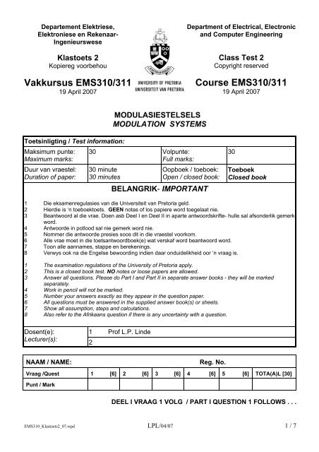
Vakkursus EMS310/311 Course EMS310/311 - Electrical, Electronic ...
Vakkursus EMS310/311 Course EMS310/311 - Electrical, Electronic ...
Vakkursus EMS310/311 Course EMS310/311 - Electrical, Electronic ...

Create successful ePaper yourself
Turn your PDF publications into a flip-book with our unique Google optimized e-Paper software.
Departement Elektriese,<br />
Elektroniese en Rekenaar-<br />
Ingenieurswese<br />
Klastoets 2<br />
Kopiereg voorbehou<br />
<strong>Vakkursus</strong> <strong>EMS310</strong>/<strong>311</strong><br />
19 April 2007<br />
Toetsinligting / Test information:<br />
Maksimum punte:<br />
Maximum marks:<br />
Duur van vraestel:<br />
Duration of paper:<br />
MODULASIESTELSELS<br />
MODULATION SYSTEMS<br />
30 Volpunte:<br />
Full marks:<br />
30 minute<br />
30 minutes<br />
Department of <strong>Electrical</strong>, <strong>Electronic</strong><br />
and Computer Engineering<br />
Oopboek / toeboek:<br />
Open / closed book:<br />
BELANGRIK- IMPORTANT<br />
Class Test 2<br />
Copyright reserved<br />
<strong>Course</strong> <strong>EMS310</strong>/<strong>311</strong><br />
19 April 2007<br />
<strong>EMS310</strong>_Klastoets2_07.wpd LPL/04/07 1 / 7<br />
30<br />
Toeboek<br />
Closed book<br />
1 Die eksamenregulasies van die Universiteit van Pretoria geld.<br />
2 Hierdie is ‘n toeboektoets. GEEN notas of los papiere word toegelaat nie.<br />
3 Beantwoord al die vrae. Doen asb Deel I en Deel II in aparte antwoordskrifte- hulle sal afsonderlik gemerk<br />
word.<br />
4 Antwoorde in potlood sal nie gemerk word nie.<br />
5 Nommer die antwoorde presies soos dit in die vraestel voorkom.<br />
6 Alle vrae moet in die toetsantwoordboek(e) wat verskaf word beantwoord word.<br />
7 Toon alle aannames, stappe en berekenings.<br />
8 Verwys ook na die Engelse bewoording indien daar onduidelikheid oor ‘n vraag is.<br />
1 The examination regulations of the University of Pretoria apply.<br />
2 This is a closed book test. NO notes or loose papers are allowed.<br />
3 Answer all questions. Please do Part I and Part II in separate answer books - they will be marked<br />
separately.<br />
4 Work in pencil will not be marked.<br />
5 Number your answers exactly as they appear in the question paper.<br />
6 All questions must be answered in the supplied answer book(s) or sheets.<br />
7 Show all assumption, steps and calculations.<br />
8 Also refer to the Afrikaans question if there is any uncertainty with a question.<br />
Dosent(e):<br />
Lecturer(s):<br />
1 Prof L.P. Linde<br />
2<br />
NAAM / NAME: Reg. No.<br />
Vraag /Quest 1 [6] 2 [6] 3 [6] 4 [6] 5 [6] TOTA(A)L [30]<br />
Punt / Mark<br />
DEEL I VRAAG 1 VOLG / PART I QUESTION 1 FOLLOWS . . .
1.<br />
1.1 Skets die blokdiagram van ‘n FSL en identifiseer die basiese substelsels of subelemente. Gee kortliks<br />
die funksie van elke boublok/substelsel. Toon alle seine en spesifiseer die ekwivalente Laplace<br />
oordragfunksie van elke element in u blokdiagram.<br />
Sketch the block diagram of a PLL and identify the basic subsystems or building blocks. Give a<br />
concise description of the function of each building block / subsystem. Show all signals and specify the<br />
equivalent Laplace transfer function of each building block in your block diagram.<br />
Fig. 1-1 FSL-blokdiagram / PLL block diagram (3)<br />
1.2 Funksie/beskrywing van elke FSL-substelsel / Function/description of each PLL subsystem:<br />
1.2.1<br />
1.2.2<br />
1.2.3<br />
<strong>EMS310</strong>_Klastoets2_07.wpd LPL/04/07 2 / 7<br />
[6]<br />
(1)<br />
(1)<br />
(1)
2 Identifiseer en skets die boublokke wat tesame die FSL fasedetektor vorm. Watter wiskundige funksie beskryf<br />
die werking van die fasedetektor? Gee ‘n uitdrukking in terme van die groothede in u fsl blokdiagram in 1.1<br />
hierbo. Skets die fasedetektor-oordragfunksie en toon aan hoe die fasedetektor-konstante bepaal word<br />
(spesifiseer eenhede!)<br />
Identify and sketch the building blocks which together form the PLL phase detector. What mathematical function<br />
best describes the operation of the phase detector? Write down an expression in terms of the quantities specified<br />
in your PLL block diagram in 1.1 above. Sketch the phase detector transfer function and show<br />
how the phase detector constant is determined (specify units!)<br />
[6]<br />
2.1 Skets fasedetektor / Sketch Phase detector (2) | Fasedetektoroordragfunksie / Phase detector transfer function (2)<br />
2.1.1 Fasedetektor ekwivalente wiskundige funksie / Phase detector equivalent mathematical function:<br />
2.1.2 Herlei fasedetektorkonstante, K D [Eenhede?] / Derive phase detector constant, K D [Units?]<br />
<strong>EMS310</strong>_Klastoets2_07.wpd LPL/04/07 3 / 7<br />
(1)<br />
(1)
3.<br />
3.1 Teken die blokdiagram van ‘n ideale basisband verwysingstelsel (sonder modulasie), met m(t) die intree-<br />
(informasie-)sein met drywing P m=S i [Watt]. Die SWGR-kanaal tel with Gauss-ruis met tweesydige<br />
DrywingsDigtheidSpektrum (DDS) N/2 [W/Hz] by. Aanvaar ‘n perfekte LDF in die ontvanger met bandwydte<br />
B$f m [Hz], waar f m die maksimum informasiefrekwensie voorstel.<br />
Draw the block diagram of an ideal reference baseband communication system (without modulation), with m(t)<br />
the input (information) signal with power P m=S i [Watt]. The AWGN channel adds white Gaussian noise with<br />
two-sided Power-Spectral-Density (PSD) N/2 [W/Hz]. Assume a perfect LPF in the receiver with bandwidth<br />
B$f m [Hz], where f m denotes the maximum information frequency.<br />
Fig. 3-1 Blokdiagram van ideale basisband verwysing-kommunikasiestelsel<br />
Block diagram of ideal reference baseband communication system. (3)<br />
3.2 Bereken die ontvangde informasie-seindrywing S i en die ruisdrywing N o by die uitgang van die<br />
basisbandontvanger, en bepaal ‘n uitdrukking vir die uitgang sein-tot-ruis-verhouding, (SNR) b.<br />
Calculate the received information signal power S i and the noise power N o at the output of the baseband<br />
receiver, and determine an expression for the output signal-to-noise-ratio, (SNR) b.<br />
Bereken P m= S i=S o [W] en N o [W], en gevolglik `n uitdrukking vir (SNR) b.<br />
Calculate P m= S i=S o [W] and N o [W], and hence an expression for (SNR) b:<br />
(SNR) b =<br />
<strong>EMS310</strong>_Klastoets2_07.wpd LPL/04/07 4 / 7<br />
[6]<br />
(3)
4 Herlei ‘n noubandmodel (tyd-uitdrukking) vir ideale bandlaatgefilterde SWGR, n(t), met tweesydige DDS N/2<br />
[W/Hz]. Gee ook `n skets van die fasordiagram van die komplekse omhulling van die ekwivalente<br />
nt ~ ()<br />
nouband basisband ruis en herlei uitdrukkings vir die infasige, nc(t), en haaksfasige, ns(t), komponente van die<br />
ruis in terme van (itv) die reële omhulling |n(t)|=| | en hoek θn [rad] van die bandlaatruis, n(t). Stel die<br />
nt ~ ()<br />
voorwaarde(s)/benadering(s) wat gemaak word om die noubandmodel vir die kanaal bandlaatruis af te lei.<br />
Derive a narrowband model (time expression) for ideal band-pass-filtered AWGN, n(t), with two-sided PSD N/2<br />
[W/Hz]. Also give a plot of the phasor diagram of the complex envelope nt ~ () of the equivalent narrowband<br />
baseband noise and derive expressions for the in-phase, nc(t), and quadrature, ns(t), components of the noise in<br />
terms of (ito) the real envelope |n(t)|=| nt ~ () | and angle θn [rad] of the band-pass noise, n(t). State the<br />
assumption/approximation(s) made to derive this (narrowband) model for the channel band-pass<br />
noise, n(t).<br />
[6]<br />
<strong>EMS310</strong>_Klastoets2_07.wpd LPL/04/07 5 / 7
5 Herlei uitdrukkings vir die ontvanger intree S/R (na die ontvanger-BDF) en die ontvanger uitgang S/R, (SNR) i<br />
and (SNR) 0 repektiewelik, in die geval van AM-DSB-OD met moduleersein m(t) en Tx en Rx draers van<br />
%2cos(ωct) en %2cos(ωct+θ), onderskeidelik, met θ=π/4 [rad]. Aanvaar `n perfekte BDF by die ontvanger en `n<br />
SWG- kanaal met tweesydige DDS N/2 [W/Hz]. Beskryf die volledige demodulasieproses analities. Hoe<br />
vergelyk die S/R-werkverrigting van hierdie AM-DSB-OD stelsel met die ideale basisband-verwysingstelsel in<br />
4 hierbo? Verklaar enige verskille.<br />
Derive expressions for the receiver input (after the Rx BPF) and the receiver output SNRs, (SNR) i and (SNR) 0,<br />
respectively, in the case of AM-DSB-SC with modulating signal m(t) and Tx and Rx carriers of %2cos(ωct) and<br />
%2cos(ωct+θ), respectively, with θ=π/4 [rad]. Assume a perfect BPF at the receiver and an AWGN channel with<br />
two-sided PSD N/2 [W/Hz]. Show the complete demodulation process analytically. How does the SNR<br />
performance of this AM-DSB-SC system compare with the ideal reference baseband system in 4 above? Explain<br />
any differences.<br />
EINDE<br />
END<br />
<strong>EMS310</strong>_Klastoets2_07.wpd LPL/04/07 6 / 7<br />
[6]
T<br />
F<br />
ω<br />
n<br />
ξ =<br />
APPENDIX A<br />
PLL IDENTITIES<br />
The following formulas are relevant to a second order PLL with passive loop filter, F(ω), with components (R 1, R 2, C). The natural<br />
angular frequency of the PLL is described by:<br />
K′ = K<br />
N<br />
⎡ K′<br />
⎤<br />
= ⎢ ⎥<br />
⎣τ<br />
T ⎦<br />
1 ⎡ K ′ ⎤<br />
⎢ ⎥<br />
2 ⎣ τ T ⎦<br />
1 2<br />
( ∆ ω )<br />
= 3<br />
2ξωn<br />
[sec]<br />
2<br />
4( ∆ f )<br />
= 3 ;<br />
B<br />
ξ = 1 = 0707 .<br />
2<br />
L<br />
2<br />
1 2<br />
[ rad / s]<br />
(1)<br />
where is the total loop gain, with N the loop division factor. The total loop filter constant is given by τT = ( R1 + R2) C .<br />
The damping constant of the PLL is given by:<br />
The -3dB bandwidth of the closed-loop transfer function, H(ω), is:<br />
[ τ + 1<br />
2 ]<br />
<strong>EMS310</strong>_Klastoets2_07.wpd LPL/04/07 7 / 7<br />
K ′<br />
2 2 2<br />
[ 2 1 2 1 1]<br />
ω− 3 = ω ξ + + ξ + +<br />
The closed-loop noise bandwidth, BL, of the PLL is given by:<br />
∞ 2<br />
dB n ( ) [ rad / s ]<br />
ω n ⎡ 1 ⎤<br />
BL= ∫ H( ω ) . df = ⎢ξ<br />
+ ⎥ [ Hz ]<br />
0<br />
2 ⎣ 4ξ<br />
⎦<br />
If the input signal frequency and phase falls within the bandwidth of the loop filter, locking will occur without cycle slipping, for a<br />
angular frequency difference of:<br />
∆ω<br />
K′<br />
. τ 2<br />
=<br />
τ + τ<br />
L n<br />
1 2<br />
≈ 2ξω [ rad/s] if K′<br />
>><br />
The maximum angular frequency difference which the PLL will be able to Pull-In (with or without cycle slipping) is approximately<br />
equal to:<br />
[ K ]<br />
1 2<br />
2<br />
∆ ω = 2 2ξω<br />
′ − ω<br />
1 2<br />
. [rad/s] (6)<br />
PI n n<br />
The maximum frequency-offset, ∆ωHI [rad/s], from the nominal VCO-frequency of ωo [rad/s], which the PLL will be able to track<br />
without cycle slipping, after it has already locked onto the input signal, is given by:<br />
∆ω HI = K′<br />
[rad / s] (7)<br />
The time it takes for a PLL to lock onto a frequency component ∆ω [rad/s] away from the nominal VCO frequency, is:<br />
(2)<br />
(3)<br />
(4)<br />
(5)<br />
(8)