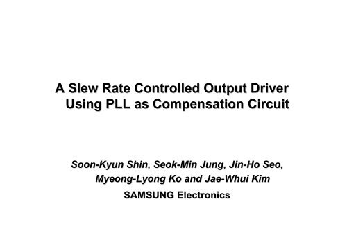
A Slew Rate Controlled Output Driver Using PLL as ... - Imec
A Slew Rate Controlled Output Driver Using PLL as ... - Imec
A Slew Rate Controlled Output Driver Using PLL as ... - Imec

Create successful ePaper yourself
Turn your PDF publications into a flip-book with our unique Google optimized e-Paper software.
A <strong>Slew</strong> <strong>Rate</strong> <strong>Controlled</strong> <strong>Output</strong> <strong>Driver</strong><br />
<strong>Using</strong> <strong>PLL</strong> <strong>as</strong> Compensation Circuit<br />
Soon-Kyun Soon Kyun Shin, Seok-Min Seok Min Jung, Jin-Ho Jin Ho Seo,<br />
Myeong-Lyong<br />
Myeong Lyong Ko and Jae-Whui Jae Whui Kim<br />
SAMSUNG Electronics
✙ Overview<br />
Outline<br />
✙ Introduction to <strong>Slew</strong> <strong>Rate</strong> Control<br />
✙ Circuits for Compensation & <strong>Slew</strong> <strong>Rate</strong> Control<br />
✙ Simulation & Test Results<br />
✙ Conclusions<br />
24 September 2002 -2/18 -<br />
ESSCIRC 2002 , Soon-Kyun Shin
✙ Applications<br />
ATA Mode<br />
Overview of ATA/ATAPI<br />
HDD, DVD-ROM, CD-ROM,CD-RW<br />
IEEE1394 to ATAPI Bridge Chip<br />
USB2.0 to ATAPI Bridge Chip<br />
Data <strong>Rate</strong><br />
(Signal Frequency)<br />
<strong>Slew</strong> <strong>Rate</strong> Specification<br />
@Load Condition<br />
33 MBps<br />
UDMA33 Min tr,tf 5ns@40pF<br />
(8.25MHz)<br />
66 MBps<br />
UDMA66 Max 1.25[V/ns]@40pF<br />
(16.5MHz)<br />
100 MBps<br />
UDMA100 0.4 ~ 1.0[V/ns]@15~40pF<br />
(25MHz)<br />
133 MBps<br />
UDMA133 0.4 ~ 1.0[V/ns]@15~40pF<br />
(33.3MHz)<br />
Cable Type<br />
40 conductor<br />
80 conductor<br />
80 conductor<br />
80 conductor<br />
24 September 2002 -3/18 -<br />
ESSCIRC 2002 , Soon-Kyun Shin
Key issues<br />
✙ <strong>Slew</strong> <strong>Rate</strong> : 0.4 ~ 1.0 [V/ns] @15~40pF<br />
Must guarantee within 2.5 times variation over PVT (<br />
Process, Voltage, Temperature) variation.<br />
Load variation is 2.67 times variation compared to15pF.<br />
<strong>Slew</strong> rate is too f<strong>as</strong>t to use feedback architecture.<br />
External resistor is not allowed.<br />
⇒ PVT compensation circuit is needed.<br />
⇒ Compensation for load variation is needed.<br />
24 September 2002 -4/18 -<br />
ESSCIRC 2002 , Soon-Kyun Shin
Voltage<br />
Voltage<br />
PAD<br />
pMOS driver<br />
Gate voltage<br />
Concept of <strong>Slew</strong> <strong>Rate</strong> Control<br />
Interval time<br />
15pF Load<br />
First step<br />
Interval time<br />
First step<br />
15pF Load<br />
Second step<br />
nMOS driver<br />
Gate voltage<br />
40pF Load<br />
40pF Load<br />
Second step<br />
PAD<br />
time<br />
time<br />
✙ The second step of gate<br />
voltage does not affect the<br />
slew rate of small load<br />
capacitance.<br />
✙ The interval time can be<br />
estimated through simulation<br />
of first voltage step over PVT<br />
variation.<br />
24 September 2002 -5/18 -<br />
ESSCIRC 2002 , Soon-Kyun Shin
TRI-STATE<br />
DATA<br />
FIN<br />
Simplified Block Diagram<br />
Ph<strong>as</strong>e<br />
Frequency<br />
Detector<br />
Tri-state<br />
Control<br />
Logic<br />
UP<br />
DOWN<br />
PC<br />
NC<br />
<strong>Slew</strong> <strong>Rate</strong><br />
Control Block<br />
Divider<br />
(1/N)<br />
Voltage<br />
<strong>Controlled</strong><br />
Oscillator<br />
24 September 2002 -6/18 -<br />
ESSCIRC 2002 , Soon-Kyun Shin<br />
VCON<br />
PG<br />
NG<br />
FOUT<br />
Tolerant & Failsafe<br />
pMOS <strong>Driver</strong><br />
Tolerant & Failsafe<br />
nMOS <strong>Driver</strong><br />
VPBIAS<br />
VNBIAS<br />
PAD
VCON<br />
Voltage <strong>Controlled</strong> Oscillator<br />
Id<br />
Ctot<br />
N : the Number of delay stage<br />
VDD<br />
VPBIAS<br />
FOUT<br />
VNBIAS<br />
24 September 2002 -7/18 -<br />
ESSCIRC 2002 , Soon-Kyun Shin<br />
f<br />
osc<br />
1<br />
= =<br />
N( t1+ t2) N<br />
I d<br />
CV<br />
tot DD<br />
fosc : oscillation frequency of VCO<br />
t1, t2 : charge and discharge time<br />
N : number of delay stage<br />
Ctot : total capacitance of each stage<br />
Vdd : supply voltage<br />
Id : bi<strong>as</strong> current
Characteristics of <strong>PLL</strong><br />
✙ <strong>PLL</strong>’s characteristics in locked condition<br />
Constant frequency is generated over PVT<br />
corners.<br />
✙ Constant frequency means that the delay time is<br />
constant in each delay stage of VCO over PVT<br />
variation.<br />
The replica of VCO’s delay stage is used in<br />
output driver’s slew rate control block.<br />
24 September 2002 -8/18 -<br />
ESSCIRC 2002 , Soon-Kyun Shin
TRI-STATE<br />
DATA<br />
FIN<br />
Simplified Block Diagram<br />
Ph<strong>as</strong>e<br />
Frequency<br />
Detector<br />
Tri-state<br />
Control<br />
Logic<br />
UP<br />
DOWN<br />
PC<br />
NC<br />
<strong>Slew</strong> <strong>Rate</strong><br />
Control Block<br />
Divider<br />
(1/N)<br />
Voltage<br />
<strong>Controlled</strong><br />
Oscillator<br />
24 September 2002 -9/18 -<br />
ESSCIRC 2002 , Soon-Kyun Shin<br />
VCON<br />
PG<br />
NG<br />
FOUT<br />
Tolerant & Failsafe<br />
pMOS <strong>Driver</strong><br />
Tolerant & Failsafe<br />
nMOS <strong>Driver</strong><br />
VPBIAS<br />
VNBIAS<br />
PAD
PC<br />
NC<br />
Control of Gate Voltage<br />
First<br />
pull down<br />
First<br />
pull up<br />
Constant Delay Stage<br />
Constant Delay Stage<br />
Second<br />
pull down<br />
Second<br />
pull up<br />
24 September 2002 - 10/18 -<br />
ESSCIRC 2002 , Soon-Kyun Shin<br />
PG<br />
NG<br />
PAD
VPBIAS<br />
PC<br />
NC<br />
VNBIAS<br />
Replica of<br />
VCO<br />
<strong>Slew</strong> <strong>Rate</strong> Control Circuit<br />
Icontrol<br />
N3 N4<br />
N1 N2<br />
P1 P2<br />
P3 P4<br />
Icontrol<br />
PG<br />
NG<br />
VBIAS<br />
N1, P1 have the same length and different<br />
width of VCO’s bi<strong>as</strong>ing MOS.<br />
Therefore, they act like current mirrors.<br />
PAD<br />
I I<br />
K K N<br />
= × =<br />
control d<br />
CV<br />
f<br />
tot DD<br />
Icontrol : sinking and sourcing current to the<br />
gate of driver MOS.<br />
K : the ratio factor of current mirror<br />
Fosc : oscillation frequency of VCO<br />
N : the number of delay stage<br />
Ctot : total capacitance of each stage<br />
Vdd : the supply voltage<br />
Id : the bi<strong>as</strong> current of VCO<br />
24 September 2002 - 11/18 -<br />
ESSCIRC 2002 , Soon-Kyun Shin<br />
osc
<strong>Slew</strong> <strong>Rate</strong> Control<br />
✙ Constant delay is generated and used in slew rate<br />
control circuit for load variation.<br />
The replica of VCO’s delay stage is used in<br />
output driver’s slew rate control block.<br />
✙ Current source is used to reduce slew rate<br />
variation over PVT variations.<br />
The same length of MOS in VCO’s delay<br />
stage is used in output driver’s slew rate<br />
control block.<br />
24 September 2002 - 12/18 -<br />
ESSCIRC 2002 , Soon-Kyun Shin
Simulation Results(3/3)<br />
✙ Simulation results of slew rate<br />
<strong>Slew</strong> <strong>Rate</strong> Simulation Results [V/ns]<br />
Specification 0.4 ~ 1.0<br />
Conventional output driver 0.305 ~ 1.216<br />
Proposed output driver 0.403 ~ 0.986<br />
24 September 2002 - 15/18 -<br />
ESSCIRC 2002 , Soon-Kyun Shin
Layout of Test Chip<br />
<strong>PLL</strong><br />
✙ Process : 0.18um 1-poly, 6-metal CMOS technology<br />
✙ <strong>Output</strong> driver : 70[um] X 401[um]<br />
Bi<strong>as</strong> Voltage<br />
<strong>Slew</strong> <strong>Rate</strong> <strong>Controlled</strong> <strong>Output</strong> <strong>Driver</strong>s<br />
✙ <strong>PLL</strong> : 421[um] X 317[um]<br />
24 September 2002 - 16/18 -<br />
ESSCIRC 2002 , Soon-Kyun Shin
15pF<br />
Me<strong>as</strong>ured Results<br />
40pF<br />
24 September 2002 - 17/18 -<br />
ESSCIRC 2002 , Soon-Kyun Shin
Conclusions<br />
✙ Compensation current is used to reduce the slew rate<br />
variation over PVT corners.<br />
✙ A constant delay time is generated to reduce the slew<br />
rate variation over load variation using replica of VCO<br />
in <strong>PLL</strong>.<br />
✙ Implemented in 0.18um CMOS and satisfied the<br />
UDMA100 specifications.<br />
✙ Simulation results and test waveforms were shown.<br />
✙ The slew rate variation over PVT and load variation is<br />
reduced using <strong>PLL</strong> <strong>as</strong> compensation circuit.<br />
24 September 2002 - 18/18 -<br />
ESSCIRC 2002 , Soon-Kyun Shin