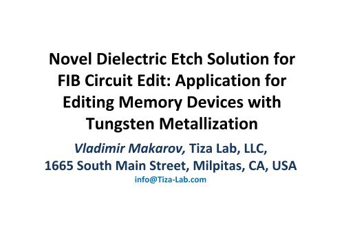
Novel Dielectric Etch Solution for FIB Circuit Edit: Application ... - Imec
Novel Dielectric Etch Solution for FIB Circuit Edit: Application ... - Imec
Novel Dielectric Etch Solution for FIB Circuit Edit: Application ... - Imec

Create successful ePaper yourself
Turn your PDF publications into a flip-book with our unique Google optimized e-Paper software.
<strong>Novel</strong> <strong>Dielectric</strong> <strong>Etch</strong> <strong>Solution</strong> <strong>for</strong><br />
<strong>FIB</strong> <strong>Circuit</strong> <strong>Edit</strong>: <strong>Application</strong> <strong>for</strong><br />
<strong>Edit</strong>ing Memory Devices with<br />
Tungsten Metallization<br />
Vladimir Makarov, Tiza Lab, LLC,<br />
1665 South Main Street, Milpitas, CA, USA<br />
info@Tiza-Lab.com
Outline<br />
• What <strong>Novel</strong> <strong>Dielectric</strong> <strong>Etch</strong> (NDE) is<br />
• What NDE was designed <strong>for</strong><br />
• <strong>Application</strong> of NDE <strong>for</strong> <strong>Circuit</strong> <strong>Edit</strong> on devices<br />
with Tungsten interconnects, compared to XeF2:<br />
- Exposure of Tungsten wires from under uneven<br />
dielectric<br />
- Rough estimation of selectivity: NDA vs XeF2<br />
• Summary
What <strong>Novel</strong> <strong>Dielectric</strong> <strong>Etch</strong> (NDE)<br />
is<br />
• <strong>Novel</strong> <strong>Dielectric</strong> <strong>Etch</strong> (NDE) is to be presented<br />
at ISTFA 2009 in San Jose, CA. All rights<br />
reserved<br />
• <strong>Novel</strong> <strong>Dielectric</strong> <strong>Etch</strong> <strong>Solution</strong> (patent pending)<br />
in contrast to XeF2, is not spontaneously<br />
aggressive to Silicon and any of sensitive low-k<br />
dielectrics.
What NDE is good <strong>for</strong><br />
• Allows circuit editing on back-side devices<br />
with open silicon<br />
XeF2<br />
NDE
What NDE is good <strong>for</strong><br />
• Allows to avoid spontaneous damaging of<br />
sensitive low-k dielectrics when coming<br />
through them
<strong>Application</strong> of NDE <strong>for</strong> <strong>Circuit</strong> <strong>Edit</strong> on<br />
devices with Tungsten interconnects<br />
• Recently, new results arrived, regarding<br />
advantages of the NDE over XeF2 in CE on<br />
devices with Tungsten metallization<br />
This presentation shows these results.
Exposure of Tungsten lines from under uneven<br />
dielectric after Copper removal<br />
XeF2
Exposure of Tungsten lines from under uneven<br />
dielectric after Copper removal<br />
NDE<br />
XeF2
When XeF 2 is in use, Tungsten lines<br />
are etched faster than dielectric!<br />
XeF2
When XeF 2 is in use, Tungsten lines<br />
are etched faster than dielectric!<br />
XeF2<br />
NDE
Testing Selectivity of <strong>Etch</strong>ing <strong>Dielectric</strong><br />
over Tungsten using NDE<br />
Purposefully<br />
over-etched W<br />
lines are still<br />
protecting<br />
dielectric under<br />
them while<br />
dielectric around<br />
is removed down<br />
to poly layer<br />
Rough estimate of<br />
selectivity is ~ 4 - 6
Summary<br />
• Using NDE <strong>for</strong> <strong>Circuit</strong> <strong>Edit</strong> of devices with<br />
Tungsten metallization provides reliable and<br />
safe method to expose Tungsten lines.<br />
• Compared to commonly used XeF2, NDA<br />
provides much higher selectivity <strong>for</strong> etching<br />
dielectric versus etching Tungsten . This<br />
reduces risk of Tungsten lines damage and<br />
disintegration