

Using External Memory with PIC24F/24H/dsPIC33F ... - Microchip
Using External Memory with PIC24F/24H/dsPIC33F ... - Microchip
Using External Memory with PIC24F/24H/dsPIC33F ... - Microchip

Create successful ePaper yourself
Turn your PDF publications into a flip-book with our unique Google optimized e-Paper software.
Author: Vidyadhar Vivekananda<br />
<strong>Microchip</strong> Technology Inc.<br />
INTRODUCTION<br />
This application note describes the methodology to use<br />
the Parallel Master Port (PMP) module to interface <strong>with</strong><br />
external data memory; either external Flash or external<br />
RAM. This application note also lists the APIs and<br />
describes how to implement different types of<br />
interfaces.<br />
<strong>Using</strong> the PMP module, the memory devices <strong>with</strong><br />
64K locations (Kbytes or K words) can be interfaced<br />
<strong>with</strong> no extra I/Os and software. This application note<br />
describes how to interface the memory devices <strong>with</strong><br />
more than 64K locations using some I/O pins and<br />
provides the required APIs.<br />
This application note describes the following topics:<br />
• “<strong>External</strong> Data <strong>Memory</strong> Interface Overview”<br />
• “Functional Implementation”<br />
• “Expansion Of <strong>External</strong> <strong>Memory</strong>”<br />
• “Reference Code”<br />
EXTERNAL DATA MEMORY<br />
INTERFACE OVERVIEW<br />
<strong>Using</strong> <strong>External</strong> Data <strong>Memory</strong> <strong>with</strong><br />
<strong>PIC24F</strong>/<strong>24H</strong>/<strong>dsPIC33F</strong> Devices<br />
The <strong>PIC24F</strong>/<strong>24H</strong>/<strong>dsPIC33F</strong> architecture supports up to<br />
64 Kbytes of internal data memory. If internal memory<br />
is insufficient, the external memory can be used. But,<br />
this external memory cannot be directly accessed by<br />
the CPU of the controller. The CPU can access through<br />
the PMP module.<br />
This section describes the topics:<br />
• Signals Required for Interfacing <strong>Memory</strong> Devices<br />
• Signals Generated by the PMP Module<br />
• Registers Associated <strong>with</strong> the PMP Module<br />
AN1210<br />
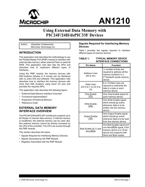
Signals Required for Interfacing <strong>Memory</strong><br />
Devices<br />
Table 1 provides the signals required to interface<br />
different types of memory devices.<br />
TABLE 1: TYPICAL MEMORY DEVICE<br />
INTERFACE CONNECTIONS<br />
Pin Name Function<br />
Address Lines<br />
(A0toAn)<br />
Data Lines<br />
(I/O 0 to 7 or I/O 0 to<br />
15)<br />
Chip Enable<br />
(CE)<br />
Write Enable<br />
(WE)<br />
Output Enable<br />
(OE)<br />
Byte Enable (A-1) and<br />
Word/Byte<br />
‘n’ number of lines are<br />
required to address all the<br />
memory locations in a<br />
2 n Kbytes/K words memory<br />
device.<br />
8 or 16 Data Lines are<br />
required to read/write the<br />
data in a byte or word<br />
memory device.<br />
One Chip Enable signal for<br />
each memory device.<br />
One Write Enable signal,<br />
which should go active<br />
whenever data is to be<br />
written into the memory<br />
device.<br />
One Output Enable signal,<br />
which should go active<br />
whenever data is to be read<br />
from the memory device.<br />
One Byte Enable signal and<br />
one Word/Byte signal, if the<br />
memory device is a 16-bit<br />
device and supports both<br />
Word and Byte modes.<br />
© 2008 <strong>Microchip</strong> Technology Inc. DS01210A-page 1
AN1210<br />
Signals Generated by the PMP Module<br />
The PMP module enables interfacing <strong>with</strong> many types<br />
of parallel devices. The module can be configured as<br />
either a master or as a slave.<br />
There are mainly two ways of interfacing read and<br />
write signals:<br />
• Read and write signals generated on two<br />
different pins (most memory devices use this<br />
type of interface).<br />
• Read and write signals generated on the same<br />
pin <strong>with</strong> separate enable signals.<br />
The PMP module in Master mode allows selection<br />
of different wait states to suit the electrical<br />
characteristics of a particular memory device<br />
The signals used to interface <strong>with</strong> the memory devices<br />
are the address bus, data bus, read signal, write<br />
signal, chip select (optional), address latch signal<br />
(if required) and byte enable (in case of 16-bit data).<br />
ADDRESS LINES<br />
PMA0 to PMA15 (up to 16 address lines are available):<br />
• PMA14 pin is multiplexed <strong>with</strong> PMCS1 pin.<br />
• PMA15 pin is multiplexed <strong>with</strong> PMCS2 pin.<br />
• Up to 64K locations can be accessed when Chip<br />
Select mode is not selected.<br />
• Up to 32K locations of memory can be accessed<br />
when only one Chip Select mode is selected.<br />
• Up to 32K locations (i.e., 16K locations x 2) of<br />
memory can be accessed when two Chip Select<br />
modes are selected.<br />
DATA LINES<br />
PMD0 to PMD7 (8 data lines):<br />
• In 8-bit operation, 8-bit data is<br />
transmitted/received through these lines.<br />
• In 16-bit operation, 16-bit data is divided into the<br />
Least Significant Byte (LSB) and Most Significant<br />
Byte (MSB). First the LSB is transmitted/received<br />
through these lines, and then the MSB.<br />
CONTROL LINES<br />
• PMCS1 and PMCS2 (up to two chip select lines)<br />
These lines are multiplexed <strong>with</strong> PMA14 and PMA15.<br />
If chip select signals are selected, the address lines<br />
are necessarily reduced.<br />
• PMWR can be used as a write line or an enable<br />
signal. To interface <strong>with</strong> a memory device, it<br />
should be used as a write line.<br />
• PMRD can be used as a read line or a read/write<br />
line. To interface <strong>with</strong> a memory device, it should<br />
be used as a read line.<br />
• PMBE is a byte enable line, used during 16-bit<br />
data operation. It goes active for MSB and<br />
inactive for LSB.<br />
• PMALL and PMALH address latch lines are<br />
required only when the address bus is<br />
multiplexed <strong>with</strong> the data bus. There are two<br />
methods of multiplexing:<br />
- Multiplexing only the lower 8-bit address<br />
lines <strong>with</strong> 8-bit data lines. In this method,<br />
PMALL is generated on the PMA0 line. This<br />
can be used to latch the lower byte of the<br />
address.<br />
- Multiplexing both the lower 8-bit and the<br />
higher 8-bit address lines <strong>with</strong> 8-bit data<br />
lines. In this method, the PMA0 becomes<br />
PMALL and PMA1 becomes PMALH.<br />
PMALH is used to latch the higher byte of<br />
the address.<br />
Figure 1 illustrates signals generated by the PMP<br />
module that are useful when interfacing <strong>with</strong> a memory<br />
device.<br />
DS01210A-page 2 © 2008 <strong>Microchip</strong> Technology Inc.
FIGURE 1: MEMORY INTERFACE PMP PINS<br />
<strong>PIC24F</strong><br />
PMP<br />
TABLE 2: MEMORY INTERFACE PMP PINS<br />
Up to 16-Bit Address (PMA)<br />
8/16-Bit Data (PMD)<br />
Write (PMWR)<br />
Read (PMRD)<br />
Up to Two Chip Selects<br />
(PMCS1 and PMCS2)<br />
Address Latch Low (PMALL)<br />
Address Latch High (PMALH)<br />
Byte Enable (PMBE)<br />
Control<br />
Signals<br />
Address Bus<br />
Data Bus<br />
Control Lines<br />
<strong>Memory</strong> Device Pins Pins Associated <strong>with</strong> PMP Module<br />
Address Lines (A0 to An) PMA0 to PMAn (up to PMA15)<br />
PMALL and PMALH (in case address is multiplexed <strong>with</strong> data)<br />
Data Lines (I/O 0 to 1/O 7 or<br />
I/O 15)<br />
PMD0 to PMD7<br />
Chip Enable (CE) PMCS2 and PMCS1<br />
Write Enable (WE) PMWR<br />
Output Enable (OE) PMRD<br />
Byte Enable (A-1) PMBE<br />
AN1210<br />
© 2008 <strong>Microchip</strong> Technology Inc. DS01210A-page 3
AN1210<br />
Registers Associated <strong>with</strong> the PMP<br />
Module<br />
The following registers are associated <strong>with</strong> the PMP<br />
module in Master mode:<br />
• PMCON – Parallel Master Port Control register<br />
• PMMODE – Parallel Master Port Mode Selection<br />
register<br />
• PMAEN – Parallel Master Port Address Enable<br />
register<br />
• PMADDR – Parallel Master Port Address register<br />
• PMDIN1 – Parallel Master Port Data register<br />
PMCON REGISTER<br />
The PMCON register controls these PMP functions:<br />
• Enables PMP module<br />
• Selects/deselects PMP module in Idle mode<br />
• Selects different modes for data address<br />
multiplexing<br />
• Enables or disables byte enable signal (PMBE)<br />
(byte enable signal is used only in 16-Bit Data<br />
mode)<br />
• Enables write signal (PMWR)<br />
• Enables read signal (PMRD)<br />
• Selects a chip select signal or higher address<br />
lines<br />
• Selects polarity of the address latch signals,<br />
PMALL and PMALH, used when address and<br />
data lines are multiplexed. (The signal polarity is<br />
the state of that signal when it is active; the signal<br />
will have the opposite state when it is Idle.)<br />
• Selects polarity of Chip Select 2 signal (PMCS2)<br />
when Chip Select 2 is used<br />
• Selects polarity of Chip Select 1 signal (PMCS1)<br />
when Chip Select 1 is used<br />
• Selects polarity of byte enable signal (PMBE)<br />
when 16-Bit Data mode is opted<br />
• Selects polarity of write signal (PMWR)<br />
• Selects polarity of read signal (PMRD)<br />
PMMODE REGISTER<br />
The PMMODE register controls these PMP functions:<br />
• Determines the status, whether the PMP module<br />
is busy or not<br />
• Selects when to set the interrupt flag<br />
• Selects either to auto-increment or decrement<br />
address<br />
• Selects 8-Bit or 16-Bit Data mode<br />
• Selects between two Master and two Slave<br />
modes. (For a memory interface, select Master<br />
mode <strong>with</strong> separate read and write signals.)<br />
• Selects different Wait periods (For more<br />
information, refer to the “Wait States and Their<br />
Usage” section.)<br />
PMAEN REGISTER<br />
The PMAEN register controls these PMP functions:<br />
• Enables Chip Select 2/Address 15<br />
(PMCS2/PMA15) port<br />
• Enables Chip Select 1/Address 14<br />
(PMCS1/PMA14) port<br />
• Enables Address 13:2 (PMA) ports<br />
• Enables Address 1/Address High Latch<br />
(PMA1/PMALH) port<br />
• Enables Address 0/Address Low Latch<br />
(PMA0/PMALL) port<br />
PMADDR REGISTER<br />
This register holds the address of the memory location<br />
to be accessed. This either remains unchanged,<br />
increments or decrements on data access as per the<br />
PMMODE configuration.<br />
PMDIN1 REGISTER<br />
This register holds the data read while reading, and<br />
holds the data to be written while writing. When the<br />
PMP is configured in 8-Bit Data mode, only the LSB of<br />
the PMDIN1 register is valid.<br />
Note: For more information on these registers,<br />
refer to the specific device data sheet.<br />
Wait States and Their Usage<br />
All memory devices have setup time, hold time and<br />
control signal width specifications. To meet these specifications,<br />
all three Wait states can be configured in the<br />
PMP module.<br />
Setup time can be configured between 1 TCY and<br />
4TCY, but the setup time is independently configurable<br />
only when the address lines and data lines are not<br />
multiplexed. When address lines and data lines are<br />
multiplexed, setup time and the width of the address<br />
phase on the data bus both are configured using a<br />
common set of bits.<br />
Hold time can also be configured between 1 TCY and<br />
4TCY.<br />
The control signals (read and write) pulse width (control<br />
signal width) can be configured between 1 TCY and<br />
15 TCY.<br />
When Wait states are disabled, setup time is set to<br />
1/4 TCY, hold time is set to 1/4 TCY, control signal width<br />
is set to 1/2 TCY and the address width on data lines<br />
(when address and data are multiplexed) is set to<br />
1TCY.<br />
Figure 14 and Figure 15 depict the effect of using the<br />
Wait states.<br />
DS01210A-page 4 © 2008 <strong>Microchip</strong> Technology Inc.
FUNCTIONAL IMPLEMENTATION<br />
This section describes the interfaces implemented in<br />
this application note. The following topics are<br />
described:<br />
• Interfacing a 64K x 8-bit memory device (<strong>with</strong><br />
chip select permanently activated)<br />
• Interfacing a 32K x 8-bit memory device<br />
• Interfacing two 16K x 8-bit memory devices<br />
• Interfacing a 32K x 16-bit word memory device<br />
AN1210<br />
Interfacing a 64K x 8-Bit <strong>Memory</strong> Device<br />
(<strong>with</strong> Chip Enable Permanently<br />
Activated)<br />
To interface a 64K x 8-bit memory device, 16 address<br />
lines are required. The PMP module can generate up<br />
to a 16-bit address (16-bit address is available only<br />
when chip select is not enabled). Figure 2 illustrates<br />
how a 64K x 8-bit memory device would be connected.<br />
Figure 4 provides a timing diagram (PMCS2 should be<br />
ignored as chip enable is permanently activated). It can<br />
be observed that each read and write operation takes<br />
one instruction cycle.<br />
Table 3 provides the register configurations for<br />
associated registers.<br />
To use the APIs provided <strong>with</strong> this application note for<br />
this configuration, uncomment the following lines in the<br />
MIDefn.h file:<br />
#define Single64KBChipNoCS<br />
#define NoAddressDataMux<br />
FIGURE 2: BLOCK DIAGRAM OF 64K x 8-BIT MEMORY DEVICE INTERFACE<br />
<strong>PIC24F</strong><br />
PMA<br />
PMD<br />
PMRD<br />
PMWR<br />
<strong>Memory</strong><br />
A<br />
D<br />
OE<br />
WR<br />
CE<br />
Address Bus<br />
Data Bus<br />
Control Lines<br />
© 2008 <strong>Microchip</strong> Technology Inc. DS01210A-page 5
AN1210<br />
TABLE 3: CONFIGURATION OF PMP REGISTERS FOR INTERFACING 64K x 8-BIT MEMORY<br />
DEVICE USING 16 ADDRESS LINES AND CHIP ENABLE PERMANENTLY<br />
ACTIVATED<br />
Register Value Description<br />
PMCON 10x0001100xxxx00 • PMP module enabled<br />
• Select to run/stop in Idle mode<br />
• Address and data on separate pins<br />
• PMBE port disabled<br />
• PMWR port enabled<br />
• PMRD port enabled<br />
• PMCS1 and PMCS2 functioning as PMA15 and PMA14<br />
• Address latch signal polarity is irrelevant (no address latch signals<br />
used)<br />
• PMCS2 polarity is irrelevant (no PMCS2 used)<br />
• PMCS1 polarity is irrelevant (no PMCS1 used)<br />
• Byte enable is irrelevant (no byte enable used)<br />
• Write strobe polarity, active-low<br />
• Read strobe polarity, active-low<br />
PMMOD 00xxx010xxxxxxxx • Busy status bit<br />
• Whether to get interrupted on read/write or not<br />
• Auto-increment/decrement or no auto-change of address<br />
• 8-Bit Data mode<br />
• Master mode <strong>with</strong> separate read and write strobes<br />
• Required data setup time<br />
• Required read/write strobe width<br />
• Required data hold time after strobe<br />
PMAEN 1111111111111111 Enable as many address line ports as required<br />
PMADDR xxxxxxxxxxxxxxxx Address register<br />
PMDIN1 N/A Data register<br />
DS01210A-page 6 © 2008 <strong>Microchip</strong> Technology Inc.
Interfacing a 32K x 8-Bit <strong>Memory</strong> Device<br />
While interfacing a 64K x 8-bit memory device, the chip<br />
enable pin of the memory device was connected to<br />
ground. If the chip select generated by the PMP is used<br />
to connect to the chip enable of the memory device,<br />
then only 15 address lines will be left, and hence, only<br />
32K x 8-bit memory device can be interfaced.<br />
In this interface all the three multiplexing modes are<br />
described. These three modes can also be used during<br />
any of the other interfaces described in this application<br />
note. The three multiplexing modes are:<br />
• No Multiplex mode (address data demultiplexed)<br />
• Partially Multiplexed mode (lower address<br />
multiplexed <strong>with</strong> data)<br />
• Fully Multiplexed mode (both lower and higher<br />
bytes of address multiplexed <strong>with</strong> data)<br />
DEMULTIPLEXED MODE<br />
AN1210<br />
In this mode, all address and data lines have separate<br />
pins. Figure 3 illustrates the interface between a<br />
32K x 8-bit memory device and a <strong>PIC24F</strong> device.<br />
Figure 4 provides a timing diagram. In Demultiplex<br />
mode, each read and write operation takes one<br />
instruction cycle.<br />
Table 4 provides the register configurations for<br />
associated registers.<br />
To use the APIs provided <strong>with</strong> this application note for<br />
this configuration, uncomment the following lines in the<br />
MIDefn.h file:<br />
#define Single32KBChip<br />
#define NoAddressDataMux<br />
FIGURE 3: 32K x 8-BIT MEMORY DEVICE INTERFACE (DEMULTIPLEXED MODE)<br />
<strong>PIC24F</strong><br />
PMA<br />
PMD<br />
PMCS2<br />
PMRD<br />
PMWR<br />
<strong>Memory</strong><br />
A<br />
D<br />
CE<br />
OE<br />
WR<br />
Address Bus<br />
Data Bus<br />
Control Lines<br />
© 2008 <strong>Microchip</strong> Technology Inc. DS01210A-page 7
AN1210<br />
TABLE 4: CONFIGURATION OF PMP REGISTERS FOR INTERFACING A 32K x 8-BIT MEMORY<br />
DEVICE (DEMULTIPLEXED MODE)<br />
Register Value Description<br />
PMCON 10x0001101x0xx00 • PMP module enabled<br />
• Select to run/stop in Idle mode<br />
• Address and data on separate pins<br />
• PMBE port disabled<br />
• PMWR port enabled<br />
• PMRD port enabled<br />
• PMCS1 functioning as PMA14 and PMCS2 as chip select<br />
• Address latch signal polarity is irrelevant (no address latch signal used)<br />
• PMCS2 polarity low<br />
• PMCS1 polarity is irrelevant (no PMCS1 used)<br />
• Byte enable polarity is irrelevant (no byte enable used)<br />
• Write strobe polarity, active-low<br />
• Read strobe polarity, active-low<br />
PMMODE 00xxx010xxxxxxxx • Busy status bit<br />
• Whether to get interrupted on read/write or not<br />
• Auto-increment/decrement or no auto-change of address<br />
• 8-Bit Data mode<br />
• Master mode <strong>with</strong> separate read and write strobes<br />
• Required data setup time<br />
• Required read/write strobe width<br />
• Required data hold time after strobe<br />
PMAEN 1111111111111111 • Enable PMCS2 port<br />
• Enable as many address line ports as required<br />
PMADDR 1xxxxxxxxxxxxxxx Address register (bit 15 enables PMCS2 and bits are address bits)<br />
PMDIN1 N/A Data register<br />
FIGURE 4: READ AND WRITE TIMING WHEN ADDRESS AND DATA ARE DEMULTIPLEXED<br />
PMCS2<br />
PMA<br />
PMD<br />
PMRD<br />
PMWR<br />
1 TCY<br />
1/2 TCY<br />
1/4 TCY<br />
DS01210A-page 8 © 2008 <strong>Microchip</strong> Technology Inc.<br />
1 TCY<br />
1/2 TCY
PARTIALLY MULTIPLEXED MODE<br />
In Partially Multiplexed mode, the lower address byte<br />
lines are multiplexed <strong>with</strong> the PMD pins. The<br />
higher address byte lines are on the PMA pins.<br />
The PMA0 pin becomes the PMALL pin; this latches<br />
the lower address byte. Therefore, seven pins<br />
(PMA) are available (free from the PMP module)<br />
for other purposes. Figure 5 illustrates the interface of<br />
a 32K x 8-bit memory device <strong>with</strong> lower address byte<br />
lines multiplexed <strong>with</strong> data lines. Figure 6 provides the<br />
timing diagram. In the Partially Multiplexed mode, each<br />
read and write operation takes two instruction cycles.<br />
AN1210<br />
Table 5 provides the register configurations for the<br />
associated registers.<br />
To use the APIs provided <strong>with</strong> this application note for<br />
this configuration, uncomment the following lines in the<br />
MIDefn.h file:<br />
#define Single32KBChip<br />
#define LowAddressDataMux<br />
FIGURE 5: 32K x 8-BIT MEMORY DEVICE INTERFACE USING PARTIALLY MULTIPLEXED MODE<br />
<strong>PIC24F</strong><br />
PMD<br />
PMALL<br />
PMA<br />
PMCS2<br />
PMRD<br />
PMWR<br />
A<br />
373<br />
D<br />
A<br />
<strong>Memory</strong><br />
© 2008 <strong>Microchip</strong> Technology Inc. DS01210A-page 9<br />
D<br />
CE<br />
OE<br />
WR<br />
Address Bus<br />
Data Bus<br />
Control Lines<br />
Address/Data Multiplexed
AN1210<br />
TABLE 5: CONFIGURATION OF PMP REGISTERS FOR INTERFACING A 32K x 8-BIT MEMORY<br />
DEVICE USING PARTIAL MULTIPLEXED MODE<br />
Register Value Description<br />
PMCON 10x010110110xx00 (1)<br />
• PMP module enabled<br />
• Select to run/stop in Idle mode<br />
• Higher address byte on separate pins and lower address byte<br />
multiplexed <strong>with</strong> data pins<br />
• PMBE port disabled<br />
• PMWR port enabled<br />
• PMRD port enabled<br />
• PMCS1 functioning as PMA14 and PMCS2 as chip select (1)<br />
• Address latch signal high (for 373 latch)<br />
• PMCS2 polarity low<br />
• PMCS1 polarity is irrelevant (no PMCS1 used)<br />
• Byte enable polarity is irrelevant (no byte enable used)<br />
• Write strobe polarity, active-low<br />
• Read strobe polarity, active-low<br />
PMMODE 00xxx010xxxxxxxx • Busy status bit<br />
• Whether to get interrupted on read/write or not<br />
• Auto-increment/decrement or no auto-change of address<br />
• 8-Bit Data mode<br />
• Master mode <strong>with</strong> separate read and write strobes<br />
• Required width of the address bus on data lines<br />
• Required read/write strobe width<br />
• Required data hold time after strobe<br />
PMAEN 1111111100000001 • Enable PMCS2 port<br />
• Enable as many higher address line ports as required<br />
• Enable PMALL port<br />
PMADDR 1xxxxxxxxxxxxxxx (1)<br />
Address register (bit 15 enables PMCS2 and bits are address<br />
bits)<br />
PMDIN1 N/A Data register<br />
Note 1: If chip select is not used, PMCON = 10x01011001xxx00 and PMADDR = xxxxxxxxxxxxxxxx.<br />
FIGURE 6: READ AND WRITE TIMING WHEN ADDRESS AND DATA LINES ARE PARTIALLY<br />
MULTIPLEXED<br />
PMCS<br />
PMA<br />
PMD<br />
PMRD<br />
PMWR<br />
PMALL<br />
1/4 TCY<br />
1 TCY<br />
1 TCY<br />
PMD<br />
PMA PMA<br />
1/2 TCY 1/2 TCY<br />
1/2 TCY<br />
1/4 TCY<br />
1/4 TCY<br />
PMD<br />
DS01210A-page 10 © 2008 <strong>Microchip</strong> Technology Inc.<br />
1 TCY<br />
1 TCY
FULLY MULTIPLEXED MODE<br />
In fully multiplexed mode, the lower and the higher<br />
address byte lines are multiplexed <strong>with</strong> PMD. The<br />
PMA0 pin becomes the PMALL pin; this latches the<br />
lower address byte. The PMA1 pin becomes the<br />
PMALH pin; this latches the higher address byte.<br />
Therefore, 13 pins (PMA) are available (free<br />
from the PMP module) for other purposes. Figure 7<br />
illustrates the interface of a 32K x 8-bit memory device,<br />
<strong>with</strong> the lower address byte lines and the higher<br />
address byte lines, multiplexed <strong>with</strong> data lines. Figure 8<br />
provides the timing diagram. In this mode, each read<br />
and write takes three instruction cycles.<br />
AN1210<br />
Table 6 provides the register configurations for<br />
associated registers.<br />
To use the APIs provided <strong>with</strong> this application note for<br />
this configuration, uncomment the following lines in the<br />
MIDefn.h file:<br />
#define Single32KBChip<br />
#define FullAddressDataMux<br />
FIGURE 7: 32K x 8-BIT MEMORY DEVICE INTERFACE USING FULLY MULTIPLEXED MODE<br />
<strong>PIC24F</strong><br />
PMD<br />
PMALL<br />
PMALH<br />
PMCS2<br />
PMRD<br />
PMWR<br />
373<br />
A<br />
<strong>Memory</strong><br />
A<br />
373<br />
D<br />
A<br />
FIGURE 8: READ AND WRITE TIMING WHEN ADDRESSES ARE FULLY MULTIPLEXED WITH<br />
DATA<br />
PMC<br />
PMD<br />
PMRD<br />
PMWR<br />
PMALL<br />
PMALH<br />
1/4 TCY<br />
PMD<br />
© 2008 <strong>Microchip</strong> Technology Inc. DS01210A-page 11<br />
D<br />
CE<br />
OE<br />
WR<br />
Address Bus<br />
Data Bus<br />
Control Lines<br />
Address/Data Multiplexed<br />
1 TCY 1 TCY 1 TCY 1 TCY 1 TCY 1 TCY<br />
PMA PMA PMA PMA<br />
PMD<br />
1/2 TCY 1/2 TCY 1/2 TCY 1/2 TCY 1/2 TCY<br />
1/2 TCY<br />
1/4 TCY 1/4 TCY<br />
1/4 TCY<br />
1/4 TCY
AN1210<br />
TABLE 6: CONFIGURATION OF PMP REGISTERS FOR INTERFACING A 32K x 8-BIT MEMORY<br />
DEVICE USING FULLY MULTIPLEXED MODE<br />
Register Value Description<br />
PMCON 10x100110110xx00 (1)<br />
• PMP module enabled<br />
• Select to run/stop in Idle mode<br />
• Lower address and higher address multiplexed <strong>with</strong> data pins<br />
• PMBE port disabled<br />
• PMWR port enabled<br />
• PMRD port enabled<br />
• PMCS1 functioning as PMA14 and PMCS2 as chip select (1)<br />
• Address latch signal polarity high (for 373 latch)<br />
• PMCS2 polarity low<br />
• PMCS1 polarity is irrelevant (no PMCS1 used)<br />
• Byte enable polarity is irrelevant (no byte enable used)<br />
• Write strobe polarity, active-low<br />
• Read strobe polarity, active-low<br />
PMMODE 00xxx010xxxxxxxx • Busy status bit<br />
• Whether to get interrupted on read/write or not<br />
• Auto-increment/decrement or no auto-change of address<br />
• 8-Bit Data mode<br />
• Master mode <strong>with</strong> separate read and write strobes<br />
• Required width of the address bus on data lines<br />
• Required read/write strobe width<br />
• Required data hold time after strobe<br />
PMAEN 1000000000000011 (1)<br />
• Enable PMCS2 port<br />
• Enable PMALH port<br />
• Enable PMALL port<br />
PMADDR 1xxxxxxxxxxxxxxx (1)<br />
Address register (bit 15 enables PMCS2 and bits are<br />
address bits)<br />
PMDIN1 N/A Data register<br />
Note 1: If chip select is not used, PMCON = 10x10011001xxx00, PMAEN = 0000000000000011 and<br />
PMADDR = xxxxxxxxxxxxxxxx.<br />
DS01210A-page 12 © 2008 <strong>Microchip</strong> Technology Inc.
Interfacing Two 16K x 8-Bit <strong>Memory</strong><br />
Devices<br />
To interface two memory devices, two chip selects are<br />
required; therefore, only 14 address bits can be<br />
generated by the PMP module. In this configuration,<br />
only two memory devices (up to 16K x 8-bit) can be<br />
connected.<br />
Figure 9 illustrates the interface of two 16-Kbyte<br />
memory devices. Figure 8 provides the timing diagram.<br />
The timing diagram illustrates only PMCS2. Similarly,<br />
when the first chip is accessed, PMCS1 becomes<br />
active instead of PMCS2.<br />
FIGURE 9: INTERFACING TWO 16K x 8-BIT MEMORY DEVICES<br />
<strong>PIC24F</strong><br />
PMD<br />
PMALL<br />
PMALH<br />
PMRD<br />
D <br />
AN1210<br />
Table 7 provides the register configurations for the<br />
associated registers.<br />
To use the APIs provided <strong>with</strong> this application note for<br />
this configuration, uncomment the following lines in the<br />
MIDefn.h file:<br />
#define Two16KBChips<br />
#define FullAddressDataMux<br />
A <br />
<strong>Memory</strong><br />
373 A<br />
373<br />
A <br />
© 2008 <strong>Microchip</strong> Technology Inc. DS01210A-page 13<br />
D<br />
PMWR WR<br />
PMCS1<br />
CE<br />
PMCS2<br />
OE<br />
<strong>Memory</strong><br />
A<br />
D<br />
OE<br />
WR<br />
CE<br />
Address Bus<br />
Data Bus<br />
Control Lines<br />
Address/Data Multiplexed
AN1210<br />
TABLE 7: CONFIGURATION OF PMP REGISTERS FOR INTERFACING TWO 16K x 8-BIT<br />
MEMORY DEVICES USING FULLY MULTIPLEXED MODE<br />
Register Value Description<br />
PMCON 10x1001110100x00 (1,2)<br />
• PMP module enabled<br />
• Select to run/stop in Idle mode<br />
• Address and data fully multiplexed (1,2)<br />
• PMBE port disabled<br />
• PMWR port enabled<br />
• PMRD port enabled<br />
• PMCS1 and PMCS2 as chip selects<br />
• Address latch signal polarity high (2)<br />
• PMCS2 polarity low<br />
• PMCS1 polarity low<br />
• Byte enable polarity is irrelevant (no byte enable used)<br />
• Write strobe polarity, active-low<br />
• Read strobe polarity, active-low<br />
PMMODE 00xxx010xxxxxxxx • Busy status bit<br />
• Whether to get interrupted on read/write or not<br />
• Auto-increment/decrement or no auto-change of address<br />
• 8-Bit Data mode<br />
• Master mode <strong>with</strong> separate read and write strobes<br />
• Required data setup time<br />
• Required read/write strobe width<br />
• Required data hold time after strobe<br />
PMAEN 1100000000000011 (1,2)<br />
• Enable PMCS2 port<br />
• Enable PMCS1 port<br />
• Enable PMALL port<br />
• Enable PMALH port<br />
PMADDR xxxxxxxxxxxxxxxx Address register (bit 15 enables PMCS2, bit 14 enables PMCS1 and<br />
bits are address bits)<br />
PMDIN1 N/A Data register<br />
Note 1: If partial address is multiplexed <strong>with</strong> data lines, PMCON = 10x0101110100x00 and<br />
PMAEN = 1111111100000001.<br />
2: If the address and data are on separate lines, PMCON = 10x0001110000x00 and<br />
PMAEN = 1111111111111111.<br />
DS01210A-page 14 © 2008 <strong>Microchip</strong> Technology Inc.
Interfacing a 32K x 16-Bit Word <strong>Memory</strong><br />
Device<br />
To interface a 16-bit memory device, 16 data lines are<br />
required. The PMP module has only 8 data lines. The<br />
16-bit data is split into two 8-bit data phases, first the<br />
LSB phase and then the MSB phase. Figure 10 and<br />
Figure 11 illustrate how to interface a 32K x 16-bit<br />
memory device.<br />
Some 16-bit memory devices support both word and<br />
byte access. These devices will have the A-1 pin, which<br />
decides the byte accessed while in Byte mode. It<br />
should be noted that we are using Byte Access mode.<br />
The PMBE pin should be connected to this pin, as<br />
illustrated in Figure 10.<br />
If the memory device supports only Word Access<br />
mode, the connections are to be made as illustrated in<br />
Figure 11.<br />
FIGURE 10: 32K x 16-BIT MEMORY DEVICE (EXAMPLE 1)<br />
<strong>PIC24F</strong><br />
PMD<br />
PMALL<br />
PMALH<br />
PMBE<br />
PMRD<br />
PMWR<br />
PMCS2<br />
AN1210<br />
Figure 12 provides the timing diagram. In 16-bit mode,<br />
each read and write takes one extra instruction cycle<br />
for the same operation in 8-bit mode. Hence, in Fully<br />
Multiplexed mode <strong>with</strong> 16-bit data, each read and write<br />
takes four instruction cycles.<br />
Table 8 provides the register configurations for the<br />
associated registers.<br />
To use the APIs provided <strong>with</strong> this application note for<br />
this configuration, uncomment the following lines in the<br />
MIDefn.h file:<br />
#define Data16bit<br />
#define HighByteEnb, if polarity of byte enable<br />
signal should be high<br />
#define FullAddressDataMux<br />
A<br />
FIGURE 11: 32K x 16-BIT MEMORY DEVICE, ADDRESS AND DATA MULTIPLEXED (EXAMPLE 2)<br />
<strong>PIC24F</strong><br />
PMD<br />
PMALL<br />
PMALH<br />
PMBE<br />
PMRD<br />
PMWR<br />
PMCS2<br />
373<br />
373<br />
373<br />
373<br />
245<br />
245<br />
A<br />
D<br />
A<br />
A<br />
A<br />
D<br />
D<br />
© 2008 <strong>Microchip</strong> Technology Inc. DS01210A-page 15<br />
D<br />
<strong>Memory</strong><br />
A-1 Word/Byte<br />
OE WR<br />
A<br />
D<br />
CE<br />
OE WR CE<br />
Address Bus<br />
Data Bus<br />
Control Lines<br />
Address/Data Multiplexed<br />
Parallel 16-Bit Device<br />
Address Bus<br />
Data Bus<br />
Control Lines<br />
Address/Data Multiplexed
AN1210<br />
TABLE 8: CONFIGURATION OF PMP REGISTERS FOR INTERFACING A 32K x 16-BIT<br />
MEMORY DEVICE USING FULLY MULTIPLEXED MODE<br />
Register Value Description<br />
PMCON 10x101110110x100 (1,2,3,4,5)<br />
• PMP module enabled<br />
• Select to run/stop in Idle mode<br />
• Address and data fully multiplexed (1,2,4,5)<br />
• PMBE port enabled<br />
• PMWR port enabled<br />
• PMRD port enabled<br />
• PMCS1 functioning as PMA14 and PMCS2 as<br />
chip select (3,4,5)<br />
• Address latch signal polarity high (2,5)<br />
• PMCS2 polarity low<br />
• PMCS1 polarity is irrelevant (3,4,5)<br />
• Byte enable polarity active-high<br />
• Write strobe polarity active-low and read strobe polarity<br />
active-low<br />
PMMODE 00xxx110xxxxxxxx • Busy status bit<br />
• Get interrupted on read/write or not<br />
• Auto-increment/decrement or no auto-change of address<br />
• 16-Bit Data mode<br />
• Master mode <strong>with</strong> separate read and write strobes<br />
• Required width of the address bus on data lines<br />
• Required read/write strobe width<br />
• Required data hold time after strobe<br />
PMAEN 1000000000000011 (1,2,3,4,5)<br />
• Enable PMCS2 port<br />
• Enable PMALH port<br />
• Enable PMALL port<br />
PMADDR 1xxxxxxxxxxxxxxx (3,4,5)<br />
Address register (bit 15 enables PMCS2 and bits are<br />
address bits)<br />
PMDIN1 N/A Data register<br />
Note 1: If partial address is multiplexed <strong>with</strong> data lines, PMCON = 10x011110110x100 and<br />
PMAEN = 1111111100000001 (this is for full 15-bit address).<br />
2: If the address and data are on separate lines, PMCON = 10x001110100x100 and<br />
PMAEN = 1111111111111111 (this is for full 15-bit address).<br />
3: If full address is multiplexed <strong>with</strong> data lines <strong>with</strong> two chip selects, PMCON = 10x1011110100100,<br />
PMAEN = 1100000000000011 (this is for full 14-bit address) and PMADDR = 11xxxxxxxxxxxxxx.<br />
4: If partial address is multiplexed <strong>with</strong> data lines <strong>with</strong> two chip selects,<br />
PMCON = 10x0111110100100, PMAEN = 1111111100000011 (this is for full 14-bit address) and<br />
PMADDR = 11xxxxxxxxxxxxxx.<br />
5: If the address and data are on separate lines <strong>with</strong> two chip selects, PMCON = 10x0011110000100,<br />
PMAEN = 1111111111111111 (this is for full 14-bit address) and PMADDR = 11xxxxxxxxxxxxxx.<br />
DS01210A-page 16 © 2008 <strong>Microchip</strong> Technology Inc.
AN1210<br />
FIGURE 12: READ TIMING WHEN THE ADDRESSES ARE FULLY MULTIPLEXED WITH DATA IN<br />
16-BIT DATA MODE<br />
PMCS2<br />
PMD<br />
PMRD<br />
PMWR<br />
PMALL<br />
PMALH<br />
PMBE<br />
1/4 TCY<br />
1 TCY 1 TCY 1 TCY<br />
1 TCY<br />
PMA PMA PMD PMD<br />
1/4 TCY<br />
1/2 TCY 1/2 TCY<br />
1/2 TCY 1/2 TCY<br />
FIGURE 13: WRITE TIMING WHEN THE ADDRESSES ARE FULLY MULTIPLEXED WITH DATA IN<br />
16-BIT DATA MODE<br />
PMCS2<br />
PMD<br />
PMRD<br />
PMWR<br />
PMALL<br />
PMALH<br />
PMBE<br />
1 TCY 1 TCY 1 TCY<br />
© 2008 <strong>Microchip</strong> Technology Inc. DS01210A-page 17<br />
1 TCY<br />
PMA PMA PMD PMD<br />
1/2 TCY 1/2 TCY<br />
1/2 TCY<br />
1/4 TCY 1/4 TCY 1/4 TCY<br />
1/2 TCY<br />
1/4 TCY
AN1210<br />
FIGURE 14: READ AND WRITE TIMING WHEN ADDRESS AND DATA ARE NOT MULTIPLEXED<br />
AND WAIT STATES ARE ENABLED<br />
PMCS2<br />
PMA<br />
PMD<br />
PMRD<br />
PMWR<br />
1 to 4 TCY (1)<br />
1 to 15 TCY (2)<br />
Note 1: Depends on setup time settings.<br />
2: Depends on control signal width settings.<br />
3: Depends on hold time settings.<br />
1 to 4 TCY (1)<br />
1 to 15 TCY (2)<br />
1 to 4 TCY (3)<br />
FIGURE 15: READ AND WRITE TIMING WHEN ADDRESS AND DATA ARE FULLY MULTIPLEXED<br />
AND WAIT STATES ARE ENABLED<br />
PMCS2<br />
PMD<br />
PMRD<br />
PMWR<br />
PMALL<br />
PMALH<br />
1 to 4 TCY (1)<br />
PMA PMA PMD PMA PMA<br />
PMD<br />
1/4 TCY<br />
1/4 TCY<br />
1 to 4 TCY (1)<br />
1/4 TCY<br />
1 to 4 TCY (1)<br />
1/4 TCY<br />
Note 1: Depends on setup time settings.<br />
2: Depends on control signal width settings.<br />
3: Depends on hold time settings.<br />
1 to 15 TCY (2)<br />
1/4 TCY<br />
1 to 4 TCY (1)<br />
1/4 TCY<br />
1 to 4 TCY (1)<br />
DS01210A-page 18 © 2008 <strong>Microchip</strong> Technology Inc.<br />
1/4 TCY<br />
1 to 4 TCY (1)<br />
1/4 TCY<br />
1 to 4 TCY (3)<br />
1 to 15 TCY (2)
EXPANSION OF EXTERNAL MEMORY<br />
<strong>External</strong> data memory can be expanded in two ways:<br />
• Interfacing single memory device of sizes more<br />
than 32 Kbytes (APIs support up to 8 Mbytes)<br />
• Interfacing multiple memory devices of 32 Kbytes<br />
each (APIs support up to 256 devices)<br />
Interfacing Single <strong>Memory</strong> Device of<br />
More than 32 Kbytes (Up to 8 Mbytes)<br />
In this interface, 15 address lines are generated by the<br />
PMP module. The higher address byte lines should be<br />
generated in the software using general purpose<br />
I/O pins.<br />
To implement this:<br />
1. Define a variable Address_High, which would<br />
have A15 to An.<br />
2. Select a port to output the higher address byte<br />
and the content of the Address_High variable.<br />
3. On a sequential read or write, increment the<br />
variable, Address_High, on every overflow of<br />
the address bus generated by the PMP module.<br />
Figure 16 illustrates the interface of a single chip <strong>with</strong> a<br />
memory size of more than 32 Kbytes.<br />
AN1210<br />
Table 9 provides the register configurations for the<br />
associated registers.<br />
To use the APIs provided <strong>with</strong> this application note for<br />
this configuration, uncomment the following lines in the<br />
MIDefn.h file:<br />
#define SingleMorethan32KBChip<br />
#define AddressHighPort LATx<br />
(where LATx can be one of LATA, LATB, LATC, LATD<br />
or LATE)<br />
#define NumberofAddedAdrsLine x<br />
(where x can be anything between 1 and 8)<br />
Note: The APIs support the expansion of the<br />
interface up to 8 Mbytes of memory<br />
(generating the address lines A22:A15).<br />
FIGURE 16: INTERFACING A SINGLE CHIP OF MORE THAN 32 Kbytes MEMORY<br />
<strong>PIC24F</strong><br />
PMD<br />
PMALL<br />
PMALH<br />
PMCS2<br />
PMRD<br />
PMWR<br />
I/O 1<br />
373<br />
373<br />
A<br />
D<br />
A<br />
I/O n An<br />
<strong>Memory</strong><br />
A<br />
© 2008 <strong>Microchip</strong> Technology Inc. DS01210A-page 19<br />
D<br />
CE<br />
OE<br />
WR<br />
A15<br />
Address Bus<br />
Data Bus<br />
Control Lines<br />
Address/Data Multiplexed
AN1210<br />
TABLE 9: CONFIGURATION OF PMP FOR INTERFACING SINGLE CHIP OF MORE THAN<br />
32 Kbytes MEMORY<br />
Register Value Description<br />
PMCON 10x100110110xx00 (1,2,3)<br />
• PMP module enabled<br />
• Select to stop/run in Idle mode<br />
• Address and data on fully multiplexed (1,2)<br />
• PMBE port disabled<br />
• PMWR port enabled<br />
• PMRD port enabled<br />
• PMCS1 functioning as PMA14 and PMCS2 as chip select (3)<br />
• Address latch signal polarity, active-high (2)<br />
• PMCS2 polarity active-low (3)<br />
• PMCS1 polarity is irrelevant (no PMCS1 used)<br />
• Byte enable polarity is irrelevant (no byte enable used)<br />
• Write strobe polarity, active-low<br />
• Read strobe polarity, active-low<br />
PMMODE 00xxx110xxxxxxxx • Busy status bit<br />
• Whether to get interrupted on read/write or not<br />
• Auto-increment/decrement or no auto-change of address<br />
• 16-Bit Data mode<br />
• Master mode <strong>with</strong> separate read and write strobes<br />
• Required width of the address bus on data lines<br />
• Required read/write strobe width<br />
• Required data hold time after strobe<br />
PMAEN 1000000000000011 (1,2)<br />
• Enable PMCS2 port<br />
• Enable PMALH port<br />
• Enable PMALL port<br />
Address_High<br />
Higher<br />
N/A Address register<br />
PMADDR 1xxxxxxxxxxxxxxx Address register (bit 15 enables PMCS2 and bits are<br />
address bits)<br />
PMDIN1 N/A Data Register<br />
Note 1: If partial address is multiplexed <strong>with</strong> data lines, PMCON = 10x01011001xxx00 and<br />
PMAEN = 1111111100000001.<br />
2: If the address and data are on separate lines, PMCON = 10x00011000xxx00 and<br />
PMAEN = 1111111111111111.<br />
3: If no chip select is used, then PMCON = 10x10011001xxx00.<br />
DS01210A-page 20 © 2008 <strong>Microchip</strong> Technology Inc.
Interfacing Multiple <strong>Memory</strong> Devices of<br />
32 Kbytes Each (Up to 256 devices)<br />
A technique to address multiple memory devices is to<br />
use a discrete demultiplexer on the chip select signal.<br />
Port I/O provide the binary encoded value to select the<br />
desired memory device.<br />
This can be implemented by defining a variable to hold<br />
the desired demultiplexer channel. Moving this value to<br />
the Port Latch register will activate the selected<br />
memory chip.<br />
For sequential read or write operations, the variable<br />
can be incremented on every PMP address overflow.<br />
To implement this, perform the following steps:<br />
1. Define a variable, Chip_Select, to selectively<br />
enable or disable different chips.<br />
2. Select a port to output the contents of the variable,<br />
Chip_Select.<br />
3. On a sequential read or write, increment the<br />
variable, Chip_Select, on every overflow of<br />
the address bus generated by the PMP module.<br />
FIGURE 17: INTERFACING MULTIPLE 32 Kbytes MEMORY DEVICES<br />
<strong>PIC24F</strong><br />
PMD<br />
PMALL<br />
PMALH<br />
PMRD<br />
PMWR<br />
PMCS2<br />
I/O 1<br />
I/O 2<br />
I/O m<br />
Demultiplexer<br />
In<br />
Sel 1<br />
Sel 2<br />
Sel m<br />
Out 1<br />
Out 2<br />
Out n<br />
AN1210<br />
Figure 17 illustrates the interface of multiple chips of<br />
32 Kbytes memory size. By using this method, the<br />
number of I/O pins required to generate the chip<br />
selects can be reduced.<br />
Table 10 provides the register configurations for the<br />
associated registers.<br />
To use the APIs provided <strong>with</strong> this application note for<br />
this configuration, uncomment the following lines in the<br />
MIDefn.h file:<br />
#define More32KBChips<br />
#define ChipSelectPort LATx<br />
(where LATx can be one of LATA, LATB, LATC, LATD<br />
or LATE)<br />
#define NumberofAddedCSLine x<br />
(where x can be anything between 1 and 3)<br />
Note: The APIs provide support expansion up to<br />
8 Mbytes of memory (generating the select<br />
signals, Sel, for the demultiplexer).<br />
A<br />
<strong>Memory</strong><br />
373 A<br />
373<br />
D<br />
A<br />
© 2008 <strong>Microchip</strong> Technology Inc. DS01210A-page 21<br />
D<br />
OE<br />
WR<br />
CE<br />
<strong>Memory</strong><br />
A<br />
D<br />
Note: The ‘m’ number of select signals required to enable ‘n’ number of memory devices where m ‘n’=2m.<br />
OE<br />
WR<br />
CE<br />
Address Bus<br />
Data Bus<br />
Control Lines<br />
Address/Data Multiplexed
AN1210<br />
TABLE 10: CONFIGURATION OF PMP REGISTERS FOR INTERFACING MULTIPLE 32 Kbytes<br />
MEMORY DEVICES<br />
Register Value Description<br />
PMCON 10x10011010xxx00 (1,2)<br />
• PMP module enabled<br />
• Select to stop/run in Idle mode<br />
• Address and data are fully multiplexed (1,2)<br />
• PMBE port disabled<br />
• PMWR port enabled<br />
• PMRD port enabled<br />
• PMCS1 functioning as PMA14 and PMCS2 as chip select<br />
• Address latch signal polarity active-high (2)<br />
• PMCS2 polarity is active-low<br />
• PMCS1 polarity is irrelevant (no PMCS1 used)<br />
• Byte enable polarity is irrelevant (no byte enable used)<br />
• Write strobe polarity, active-low<br />
• Read strobe polarity, active-low<br />
PMMODE 00xxx110xxxxxxxx • Busy status bit<br />
• Whether to get interrupted on read/write or not<br />
• Auto-increment/decrement or no auto-change of address<br />
• 16-Bit Data mode<br />
• Master mode <strong>with</strong> separate read and write strobes<br />
• Required data setup time<br />
• Required read/write strobe width<br />
• Required data hold time after strobe<br />
PMAEN 1000000000000011 (1,2)<br />
• Enable PMCS2 port<br />
• Enable PMALH port<br />
• Enable PMALL port<br />
PMADDR 1xxxxxxxxxxxxxx Address register (bit 15 enables PMCS2 and bits are<br />
address bits)<br />
PMDIN1 N/A Data register<br />
Chip_Select N/A Current Chip_Select information<br />
Note 1: If partial address is multiplexed <strong>with</strong> data lines, PMCON = 10x01011001xxx00 and<br />
PMAEN = 1111111100000001.<br />
2: If the address and data are on separate lines, PMCON = 10x00011000xxx00 and<br />
PMAEN = 1111111111111111.<br />
DS01210A-page 22 © 2008 <strong>Microchip</strong> Technology Inc.
REFERENCE CODE<br />
This section describes the APIs provided as reference<br />
code to interface different types of memory devices.<br />
To implement the interfaces described in this<br />
application note, the following APIs are provided:<br />
• PMPInit()<br />
Initializes the PMP module per the macros defined in<br />
the MIDefn.h file.<br />
• MemByteRead()<br />
Returns a byte read from the specified memory<br />
address location.<br />
• MemBulkRead()<br />
Reads the specified length of sequential data from<br />
the specified memory location and stores it at a<br />
specified array.<br />
• MemByteWrite()<br />
Writes the byte passed into the specified memory<br />
location.<br />
• MemBulkWrite()<br />
Writes the specified length of data stored in an array<br />
into the memory locations from the specified<br />
address.<br />
To use these APIs, add the MemInterface.c,<br />
MemInterface.h and MIDefn.h files to your project.<br />
Edit the MIDefn.h file as required.<br />
The selections are:<br />
<strong>Memory</strong> size and number of chips:<br />
#define Single64KBChipNoCS<br />
#define Single32KBChip<br />
#define Two16KBChips<br />
#define SingleMorethan32KBChip<br />
#define More32KBChips<br />
Select the required macros by uncommenting the<br />
macro name and comment the remaining four.<br />
For example:<br />
• To interface a 64-Kbyte memory chip, uncomment<br />
#define Single64KBChipNoCS and comment<br />
the rest.<br />
• To interface a 32-Kbyte memory chip, uncomment<br />
#define Single32KBChip and comment the<br />
rest.<br />
• To interface two 16-Kbyte memory chips,<br />
uncomment #define Two16KBChips, and<br />
comment the rest.<br />
• To interface a memory chip of more than<br />
32 Kbytes, uncomment<br />
#define SingleMorethan32KBChip and<br />
comment the rest.<br />
• To interface more 32-Kbyte memory, uncomment<br />
#define More32KBChips and comment the<br />
rest.<br />
AN1210<br />
<strong>Memory</strong> chip width 8-bit/16-bit:<br />
#define Data16bit<br />
Comment if 8-bit chip is used; uncomment if 16-bit chip<br />
is used.<br />
#define HighByteEnb<br />
(applicable only when in 16-bit mode)<br />
Comment this if active-low byte enable signal is<br />
required.<br />
Address/Data Multiplex mode:<br />
#define AddressDataNoMux<br />
#define LowAddressDataMux<br />
#define FullAddressDataMux<br />
Keep the required macro uncommented and comment<br />
the other two.<br />
For example:<br />
• To generate address and data on separate pins,<br />
uncomment #define AddressDataNoMux and<br />
comment the rest.<br />
• To multiplex only the lower address byte <strong>with</strong> the<br />
data pins, uncomment<br />
#define LowAddressDataMux and comment<br />
the rest.<br />
• To multiplex both the lower and higher address<br />
bytes <strong>with</strong> the data pins, uncomment<br />
#define FullAddressDataMux and comment<br />
the rest.<br />
Setup time, hold time and control signal width:<br />
#define SetDataSetupWait_TCY x<br />
(where x = 1/2/3/4)<br />
#define SetControlWidthWait_TCY x<br />
(where x = 0/1/…/15)<br />
#define SetDataHoldWait_TCY x<br />
(where x = 1/2/3/4)<br />
Select the setup time from one of four options (1 TCY to<br />
4TCY).<br />
Select the hold time from one of the four options (1 TCY<br />
to 4 TCY).<br />
To select the required setup time, write the count (number<br />
of TCY) against #define SetDataSetupWait_TCY.<br />
To select the required hold time, write the count<br />
(number of TCY) against<br />
#define SetDataHoldWait_TCY.<br />
Select the control signal width from one of 16 options<br />
(1 TCY to 16 TCY).<br />
To select the required control signal width, write the<br />
count (number of TCY) against<br />
#define SetControlWidthWait_TCY.<br />
© 2008 <strong>Microchip</strong> Technology Inc. DS01210A-page 23
AN1210<br />
Port selection for memory extension:<br />
To use single chip higher memory device and to select<br />
the port for generating the higher address byte,<br />
#define AddressHighPort LATx<br />
(where LATx = LATA/LATB/LATC/LATD/LATE)<br />
To specify the number of additional address lines<br />
required,<br />
#define NumberofAdded AdrsLine x<br />
(where x = anything between 1 and 8)<br />
To use multiple 32-Kbyte devices and to select the port<br />
for generating the select signal for the demultiplexer,<br />
#define ChipSelectPort LATx<br />
(where LATx = LATA/LATB/LATC/LATD/LATE)<br />
TABLE 11: APIs PROVIDED in MemInterface.c FILE<br />
To specify the number of select lines required,<br />
#define NumberofAddedCSLine x<br />
(where x = anything between 1 and 3)<br />
Table 11 provides and describes the APIs.<br />
Note: While using a single memory device,<br />
higher than 32 Kbytes, the additional<br />
address lines (above A14) should be generated<br />
by the software on general purpose<br />
I/O pins; while using multiple memory<br />
devices of 32 Kbytes, the select signals for<br />
the demultiplexer should be generated by<br />
the software on general purpose I/O pins.<br />
Function Description Inputs Outputs<br />
PMPInit() Initializes the PMP module and also<br />
the port directions if required, as<br />
defined in the MIDefn.h file.<br />
MemByteRead() Reads a byte from a specified<br />
location.<br />
MemBulkRead() Reads a specified number of bytes<br />
starting from a specified location and<br />
saves them from a specified pointer<br />
location.<br />
None None<br />
<strong>Memory</strong> location address (unsigned<br />
long)<br />
<strong>Memory</strong> location address<br />
(unsigned long)<br />
Number of bytes to be read<br />
(unsigned int)<br />
Destination pointer<br />
(unsigned char *)<br />
MemByteWrite() Writes a byte at a specified location. <strong>Memory</strong> location address<br />
(unsigned long)<br />
Data (unsigned char)<br />
MemBulkWrite() Writes a specified number of bytes<br />
starting from a specified location.<br />
<strong>Memory</strong> location address<br />
(unsigned long)<br />
Number of bytes to be written<br />
(unsigned int)<br />
Source Pointer (unsigned char *)<br />
Note: For the flowcharts of these APIs, refer to Figure 18 through Figure 23.<br />
Read data<br />
(char)<br />
DS01210A-page 24 © 2008 <strong>Microchip</strong> Technology Inc.<br />
None<br />
None<br />
None
<strong>Memory</strong> Interface Application File<br />
Example<br />
To use these APIs:<br />
1. Write an application file.<br />
2. Call it API.<br />
The APIs are in the MemInterface.c file.<br />
3. Add this file to the project folder <strong>with</strong> the<br />
application file.<br />
4. Uncomment the required definitions in the<br />
MIDefn.h file.<br />
5. Include the header file, MemInterface.h, in<br />
the application file.<br />
FIGURE 18: PMP MEMORY INTERFACE EXAMPLE FLOWCHART<br />
Start<br />
Initialize PMP Module to<br />
Interface <strong>with</strong> <strong>Memory</strong><br />
Write into <strong>Memory</strong> Device<br />
Write till Write Time is Over<br />
Read from <strong>Memory</strong> Device<br />
Stop<br />
AN1210<br />
An example file, MemIntfExample.c, is provided<br />
along <strong>with</strong> this application note. This file describes how<br />
to use the APIs to access (read and write) the external<br />
memory device. Figure 18 illustrates the flow of this<br />
example file.<br />
© 2008 <strong>Microchip</strong> Technology Inc. DS01210A-page 25
AN1210<br />
PMPInit API<br />
The API, PMPInit, initializes the PMP module as per<br />
the definitions in the file, MIDefn.h. There are no<br />
inputs for this API; this API returns nothing. This API<br />
takes all inputs from the MIDefn.h file. Figure 19<br />
illustrates the flow of the PMPInit API.<br />
FIGURE 19: PMPInit API FLOWCHART<br />
PMPInit<br />
Select mode to have read and write strobes on two different pins.<br />
Select required setup time, hold time and strobe width.<br />
Enable read and write strobe ports.<br />
Select address/data multiplexing as defined in the macros in Memdefn.h file.<br />
If 16-bit data is selected, enable byte enable port.<br />
If the address and data are multiplexed, select the polarity high for the<br />
Address Latch Enable signals (ALEL/ALEH).<br />
Select the polarity of the chip select, read and write signals as low.<br />
Byte enable is used; otherwise, select the polarity high.<br />
Enable required ports for address, chip select, and address latch enable.<br />
Drive the I/O ports used for chip select high and those used for address bus low.<br />
Configure these I/O ports as outputs. If these pins have an analog function, configure them as digital.<br />
Return<br />
DS01210A-page 26 © 2008 <strong>Microchip</strong> Technology Inc.
MemByteRead API<br />
The API, MemByteRead, reads a byte from the specified<br />
address. The inputs for this API are the memory<br />
address (24 bits) from where the data has to be read.<br />
This API returns the data read (8 bits). Figure 20<br />
illustrates the flow of the MemByteRead API.<br />
FIGURE 20: MemByteRead API FLOWCHART<br />
MemByteRead<br />
Load address_low to Address register (PMADDR) and<br />
address_high to Address High register.<br />
Enable the chip select port of the respective chip select.<br />
Is PMP<br />
Busy?<br />
Read PMP Data (Dummy Read)<br />
Is PMP<br />
Busy?<br />
Read PMP Data<br />
Return Read<br />
High<br />
AN1210<br />
© 2008 <strong>Microchip</strong> Technology Inc. DS01210A-page 27<br />
No<br />
No<br />
Yes<br />
Yes
AN1210<br />
MemBulkRead API<br />
The API MemBulkRead reads a sequence of a<br />
specified length of data from the specified address, and<br />
stores it in a specified array. The inputs for this API are<br />
the starting memory address (24 bits) from where the<br />
data has to be read, the number of data bytes (maximum<br />
64 Kbytes) to be read and the address of the<br />
array (of char) where the read data needs to be<br />
stored. This API returns nothing; it stores the read data<br />
in the passed array. Figure 20 illustrates the flow of the<br />
MemBulkRead API.<br />
FIGURE 21: MemBulkRead API FLOWCHART<br />
MemBulkRead<br />
Select address auto-increment.<br />
Load address_low to Address register (PMADDR) and<br />
address_high to Address High register.<br />
Enable the chip select port of the respective chip select.<br />
Is PMP<br />
Busy?<br />
Read PMP Data (Dummy Read)<br />
Is Buffer<br />
Full?<br />
No<br />
Is PMP<br />
Busy?<br />
No<br />
No<br />
Read PMP Data and<br />
Save in Buffer<br />
Load the address_high to Address High register.<br />
Enable the chip select port of the respective chip select.<br />
DS01210A-page 28 © 2008 <strong>Microchip</strong> Technology Inc.<br />
Yes<br />
Yes<br />
Yes<br />
Return
MemByteWrite API<br />
The API, MemByteWrite, writes a byte to the specified<br />
address. The inputs for this API are the memory<br />
address (24 bits) where the data has to be written and<br />
the data (8 bits) that needs to be written. This API<br />
returns nothing. Figure 22 illustrates the flow of the<br />
MemByteWrite API.<br />
FIGURE 22: MemByteWrite API FLOWCHART<br />
MemByteWrite<br />
Load the address_low to Address register (PMADDR) and<br />
address_high to Address High register.<br />
Enable the chip select port of the respective chip select.<br />
Is PMP<br />
Busy?<br />
Write PMP Data<br />
Return<br />
AN1210<br />
© 2008 <strong>Microchip</strong> Technology Inc. DS01210A-page 29<br />
No<br />
Yes
AN1210<br />
MemBulkWrite API<br />
The API, MemBulkWrite, writes a sequence of a<br />
specified length of bytes which is stored in an array<br />
from the specified address. The inputs for this API are,<br />
the starting memory address (24 bits) from where the<br />
data has to be written, the number of data bytes to be<br />
written (maximum 64 Kbytes) and the address of the<br />
array (of char) where the data to be written is stored.<br />
This API returns nothing. Figure 23 illustrates the flow<br />
of the MemBulkWrite API.<br />
FIGURE 23: MemBulkWrite API FLOWCHART<br />
MemBulkWrite<br />
Load address_low to Address register (PMADDR)<br />
and address_high to Address High register.<br />
Enable the chip select port of the respective chip select.<br />
Is Buffer<br />
Empty?<br />
Is PMP<br />
Busy?<br />
Write PMP Data<br />
Load address_high to Address High register.<br />
Enable the chip select port of the respective chip select.<br />
No<br />
No<br />
DS01210A-page 30 © 2008 <strong>Microchip</strong> Technology Inc.<br />
Yes<br />
Yes<br />
Return
CONCLUSION<br />
This application note discusses different ways of<br />
interfacing the memory device <strong>with</strong> the PMP module.<br />
There are merits and demerits of each interface type.<br />
One should select the appropriate interface type that<br />
suits the application most. The APIs provided can be<br />
easily used to interface memory <strong>with</strong> PMP. One has to<br />
set the definitions as per the requirements in the<br />
MIDefn.h file. The MemIntfExample.c file is an<br />
example file that describes how to use the APIs. All the<br />
APIs are provided in the MemInterface.c file.<br />
Refer to Section 13. “Parallel Master Port (PMP)” in<br />
the “<strong>PIC24F</strong> Family Reference Manual” for more<br />
information.<br />
AN1210<br />
© 2008 <strong>Microchip</strong> Technology Inc. DS01210A-page 31
AN1210<br />
NOTES:<br />
DS01210A-page 32 © 2008 <strong>Microchip</strong> Technology Inc.
Note the following details of the code protection feature on <strong>Microchip</strong> devices:<br />
• <strong>Microchip</strong> products meet the specification contained in their particular <strong>Microchip</strong> Data Sheet.<br />
• <strong>Microchip</strong> believes that its family of products is one of the most secure families of its kind on the market today, when used in the<br />
intended manner and under normal conditions.<br />
• There are dishonest and possibly illegal methods used to breach the code protection feature. All of these methods, to our<br />
knowledge, require using the <strong>Microchip</strong> products in a manner outside the operating specifications contained in <strong>Microchip</strong>’s Data<br />
Sheets. Most likely, the person doing so is engaged in theft of intellectual property.<br />
• <strong>Microchip</strong> is willing to work <strong>with</strong> the customer who is concerned about the integrity of their code.<br />
• Neither <strong>Microchip</strong> nor any other semiconductor manufacturer can guarantee the security of their code. Code protection does not<br />
mean that we are guaranteeing the product as “unbreakable.”<br />
Code protection is constantly evolving. We at <strong>Microchip</strong> are committed to continuously improving the code protection features of our<br />
products. Attempts to break <strong>Microchip</strong>’s code protection feature may be a violation of the Digital Millennium Copyright Act. If such acts<br />
allow unauthorized access to your software or other copyrighted work, you may have a right to sue for relief under that Act.<br />
Information contained in this publication regarding device<br />
applications and the like is provided only for your convenience<br />
and may be superseded by updates. It is your responsibility to<br />
ensure that your application meets <strong>with</strong> your specifications.<br />
MICROCHIP MAKES NO REPRESENTATIONS OR<br />
WARRANTIES OF ANY KIND WHETHER EXPRESS OR<br />
IMPLIED, WRITTEN OR ORAL, STATUTORY OR<br />
OTHERWISE, RELATED TO THE INFORMATION,<br />
INCLUDING BUT NOT LIMITED TO ITS CONDITION,<br />
QUALITY, PERFORMANCE, MERCHANTABILITY OR<br />
FITNESS FOR PURPOSE. <strong>Microchip</strong> disclaims all liability<br />
arising from this information and its use. Use of <strong>Microchip</strong><br />
devices in life support and/or safety applications is entirely at<br />
the buyer’s risk, and the buyer agrees to defend, indemnify and<br />
hold harmless <strong>Microchip</strong> from any and all damages, claims,<br />
suits, or expenses resulting from such use. No licenses are<br />
conveyed, implicitly or otherwise, under any <strong>Microchip</strong><br />
intellectual property rights.<br />
Trademarks<br />
The <strong>Microchip</strong> name and logo, the <strong>Microchip</strong> logo, Accuron,<br />
dsPIC, KEELOQ, KEELOQ logo, MPLAB, PIC, PICmicro,<br />
PICSTART, rfPIC and SmartShunt are registered trademarks<br />
of <strong>Microchip</strong> Technology Incorporated in the U.S.A. and other<br />
countries.<br />
FilterLab, Linear Active Thermistor, MXDEV, MXLAB,<br />
SEEVAL, SmartSensor and The Embedded Control Solutions<br />
Company are registered trademarks of <strong>Microchip</strong> Technology<br />
Incorporated in the U.S.A.<br />
Analog-for-the-Digital Age, Application Maestro, CodeGuard,<br />
dsPICDEM, dsPICDEM.net, dsPICworks, dsSPEAK, ECAN,<br />
ECONOMONITOR, FanSense, In-Circuit Serial<br />
Programming, ICSP, ICEPIC, Mindi, MiWi, MPASM, MPLAB<br />
Certified logo, MPLIB, MPLINK, mTouch, PICkit, PICDEM,<br />
PICDEM.net, PICtail, PIC 32 logo, PowerCal, PowerInfo,<br />
PowerMate, PowerTool, REAL ICE, rfLAB, Select Mode, Total<br />
Endurance, UNI/O, WiperLock and ZENA are trademarks of<br />
<strong>Microchip</strong> Technology Incorporated in the U.S.A. and other<br />
countries.<br />
SQTP is a service mark of <strong>Microchip</strong> Technology Incorporated<br />
in the U.S.A.<br />
All other trademarks mentioned herein are property of their<br />
respective companies.<br />
© 2008, <strong>Microchip</strong> Technology Incorporated, Printed in the<br />
U.S.A., All Rights Reserved.<br />
Printed on recycled paper.<br />
<strong>Microchip</strong> received ISO/TS-16949:2002 certification for its worldwide<br />
headquarters, design and wafer fabrication facilities in Chandler and<br />
Tempe, Arizona; Gresham, Oregon and design centers in California<br />
and India. The Company’s quality system processes and procedures<br />
are for its PIC ® MCUs and dsPIC ® DSCs, KEELOQ ® code hopping<br />
devices, Serial EEPROMs, microperipherals, nonvolatile memory and<br />
analog products. In addition, <strong>Microchip</strong>’s quality system for the design<br />
and manufacture of development systems is ISO 9001:2000 certified.<br />
© 2008 <strong>Microchip</strong> Technology Inc. DS01210A-page 33
AMERICAS<br />
Corporate Office<br />
2355 West Chandler Blvd.<br />
Chandler, AZ 85224-6199<br />
Tel: 480-792-7200<br />
Fax: 480-792-7277<br />
Technical Support:<br />
http://support.microchip.com<br />
Web Address:<br />
www.microchip.com<br />
Atlanta<br />
Duluth, GA<br />
Tel: 678-957-9614<br />
Fax: 678-957-1455<br />
Boston<br />
Westborough, MA<br />
Tel: 774-760-0087<br />
Fax: 774-760-0088<br />
Chicago<br />
Itasca, IL<br />
Tel: 630-285-0071<br />
Fax: 630-285-0075<br />
Dallas<br />
Addison, TX<br />
Tel: 972-818-7423<br />
Fax: 972-818-2924<br />
Detroit<br />
Farmington Hills, MI<br />
Tel: 248-538-2250<br />
Fax: 248-538-2260<br />
Kokomo<br />
Kokomo, IN<br />
Tel: 765-864-8360<br />
Fax: 765-864-8387<br />
Los Angeles<br />
Mission Viejo, CA<br />
Tel: 949-462-9523<br />
Fax: 949-462-9608<br />
Santa Clara<br />
Santa Clara, CA<br />
Tel: 408-961-6444<br />
Fax: 408-961-6445<br />
Toronto<br />
Mississauga, Ontario,<br />
Canada<br />
Tel: 905-673-0699<br />
Fax: 905-673-6509<br />
Worldwide Sales and Service<br />
ASIA/PACIFIC<br />
Asia Pacific Office<br />
Suites 3707-14, 37th Floor<br />
Tower 6, The Gateway<br />
Harbour City, Kowloon<br />
Hong Kong<br />
Tel: 852-2401-1200<br />
Fax: 852-2401-3431<br />
Australia - Sydney<br />
Tel: 61-2-9868-6733<br />
Fax: 61-2-9868-6755<br />
China - Beijing<br />
Tel: 86-10-8528-2100<br />
Fax: 86-10-8528-2104<br />
China - Chengdu<br />
Tel: 86-28-8665-5511<br />
Fax: 86-28-8665-7889<br />
China - Hong Kong SAR<br />
Tel: 852-2401-1200<br />
Fax: 852-2401-3431<br />
China - Nanjing<br />
Tel: 86-25-8473-2460<br />
Fax: 86-25-8473-2470<br />
China - Qingdao<br />
Tel: 86-532-8502-7355<br />
Fax: 86-532-8502-7205<br />
China - Shanghai<br />
Tel: 86-21-5407-5533<br />
Fax: 86-21-5407-5066<br />
China - Shenyang<br />
Tel: 86-24-2334-2829<br />
Fax: 86-24-2334-2393<br />
China - Shenzhen<br />
Tel: 86-755-8203-2660<br />
Fax: 86-755-8203-1760<br />
China - Wuhan<br />
Tel: 86-27-5980-5300<br />
Fax: 86-27-5980-5118<br />
China - Xiamen<br />
Tel: 86-592-2388138<br />
Fax: 86-592-2388130<br />
China - Xian<br />
Tel: 86-29-8833-7252<br />
Fax: 86-29-8833-7256<br />
China - Zhuhai<br />
Tel: 86-756-3210040<br />
Fax: 86-756-3210049<br />
ASIA/PACIFIC<br />
India - Bangalore<br />
Tel: 91-80-4182-8400<br />
Fax: 91-80-4182-8422<br />
India - New Delhi<br />
Tel: 91-11-4160-8631<br />
Fax: 91-11-4160-8632<br />
India - Pune<br />
Tel: 91-20-2566-1512<br />
Fax: 91-20-2566-1513<br />
Japan - Yokohama<br />
Tel: 81-45-471- 6166<br />
Fax: 81-45-471-6122<br />
Korea - Daegu<br />
Tel: 82-53-744-4301<br />
Fax: 82-53-744-4302<br />
Korea - Seoul<br />
Tel: 82-2-554-7200<br />
Fax: 82-2-558-5932 or<br />
82-2-558-5934<br />
Malaysia - Kuala Lumpur<br />
Tel: 60-3-6201-9857<br />
Fax: 60-3-6201-9859<br />
Malaysia - Penang<br />
Tel: 60-4-227-8870<br />
Fax: 60-4-227-4068<br />
Philippines - Manila<br />
Tel: 63-2-634-9065<br />
Fax: 63-2-634-9069<br />
Singapore<br />
Tel: 65-6334-8870<br />
Fax: 65-6334-8850<br />
Taiwan - Hsin Chu<br />
Tel: 886-3-572-9526<br />
Fax: 886-3-572-6459<br />
Taiwan - Kaohsiung<br />
Tel: 886-7-536-4818<br />
Fax: 886-7-536-4803<br />
Taiwan - Taipei<br />
Tel: 886-2-2500-6610<br />
Fax: 886-2-2508-0102<br />
Thailand - Bangkok<br />
Tel: 66-2-694-1351<br />
Fax: 66-2-694-1350<br />
EUROPE<br />
Austria - Wels<br />
Tel: 43-7242-2244-39<br />
Fax: 43-7242-2244-393<br />
Denmark - Copenhagen<br />
Tel: 45-4450-2828<br />
Fax: 45-4485-2829<br />
France - Paris<br />
Tel: 33-1-69-53-63-20<br />
Fax: 33-1-69-30-90-79<br />
Germany - Munich<br />
Tel: 49-89-627-144-0<br />
Fax: 49-89-627-144-44<br />
Italy - Milan<br />
Tel: 39-0331-742611<br />
Fax: 39-0331-466781<br />
Netherlands - Drunen<br />
Tel: 31-416-690399<br />
Fax: 31-416-690340<br />
Spain - Madrid<br />
Tel: 34-91-708-08-90<br />
Fax: 34-91-708-08-91<br />
UK - Wokingham<br />
Tel: 44-118-921-5869<br />
Fax: 44-118-921-5820<br />
01/02/08<br />
DS01210A-page 34 © 2008 <strong>Microchip</strong> Technology Inc.


