

Using External Memory with PIC24F/24H/dsPIC33F ... - Microchip
Using External Memory with PIC24F/24H/dsPIC33F ... - Microchip
Using External Memory with PIC24F/24H/dsPIC33F ... - Microchip

Create successful ePaper yourself
Turn your PDF publications into a flip-book with our unique Google optimized e-Paper software.
AN1210<br />
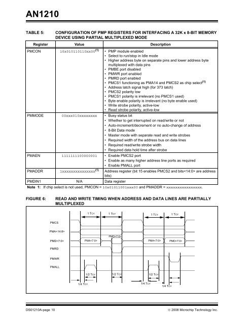
TABLE 5: CONFIGURATION OF PMP REGISTERS FOR INTERFACING A 32K x 8-BIT MEMORY<br />
DEVICE USING PARTIAL MULTIPLEXED MODE<br />
Register Value Description<br />
PMCON 10x010110110xx00 (1)<br />
• PMP module enabled<br />
• Select to run/stop in Idle mode<br />
• Higher address byte on separate pins and lower address byte<br />
multiplexed <strong>with</strong> data pins<br />
• PMBE port disabled<br />
• PMWR port enabled<br />
• PMRD port enabled<br />
• PMCS1 functioning as PMA14 and PMCS2 as chip select (1)<br />
• Address latch signal high (for 373 latch)<br />
• PMCS2 polarity low<br />
• PMCS1 polarity is irrelevant (no PMCS1 used)<br />
• Byte enable polarity is irrelevant (no byte enable used)<br />
• Write strobe polarity, active-low<br />
• Read strobe polarity, active-low<br />
PMMODE 00xxx010xxxxxxxx • Busy status bit<br />
• Whether to get interrupted on read/write or not<br />
• Auto-increment/decrement or no auto-change of address<br />
• 8-Bit Data mode<br />
• Master mode <strong>with</strong> separate read and write strobes<br />
• Required width of the address bus on data lines<br />
• Required read/write strobe width<br />
• Required data hold time after strobe<br />
PMAEN 1111111100000001 • Enable PMCS2 port<br />
• Enable as many higher address line ports as required<br />
• Enable PMALL port<br />
PMADDR 1xxxxxxxxxxxxxxx (1)<br />
Address register (bit 15 enables PMCS2 and bits are address<br />
bits)<br />
PMDIN1 N/A Data register<br />
Note 1: If chip select is not used, PMCON = 10x01011001xxx00 and PMADDR = xxxxxxxxxxxxxxxx.<br />
FIGURE 6: READ AND WRITE TIMING WHEN ADDRESS AND DATA LINES ARE PARTIALLY<br />
MULTIPLEXED<br />
PMCS<br />
PMA<br />
PMD<br />
PMRD<br />
PMWR<br />
PMALL<br />
1/4 TCY<br />
1 TCY<br />
1 TCY<br />
PMD<br />
PMA PMA<br />
1/2 TCY 1/2 TCY<br />
1/2 TCY<br />
1/4 TCY<br />
1/4 TCY<br />
PMD<br />
DS01210A-page 10 © 2008 <strong>Microchip</strong> Technology Inc.<br />
1 TCY<br />
1 TCY


