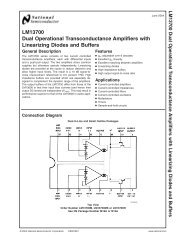
PSoC™ Mixed-Signal Array Final Data Sheet - svn
PSoC™ Mixed-Signal Array Final Data Sheet - svn
PSoC™ Mixed-Signal Array Final Data Sheet - svn

You also want an ePaper? Increase the reach of your titles
YUMPU automatically turns print PDFs into web optimized ePapers that Google loves.
CY8C29x66 <strong>Final</strong> <strong>Data</strong> <strong>Sheet</strong> 3. Electrical Specifications<br />
3.4.6 AC External Clock Specifications<br />
The following tables list guaranteed maximum and minimum specifications for the voltage and temperature ranges: 4.75V to 5.25V<br />
and -40°C ≤ T A ≤ 85°C, or 3.0V to 3.6V and -40°C ≤ T A ≤ 85°C, respectively. Typical parameters apply to 5V and 3.3V at 25°C and<br />
are for design guidance only.<br />
Table 3-23: 5V AC External Clock Specifications<br />
Symbol Description Min Typ Max Units Notes<br />
FOSCEXT Frequency 0.093 – 24.6 MHz<br />
– High Period 20.6 – 5300 ns<br />
– Low Period 20.6 – – ns<br />
– Power Up IMO to Switch 150 – – µs<br />
Table 3-24: 3.3V AC External Clock Specifications<br />
Symbol Description Min Typ Max Units Notes<br />
FOSCEXT Frequency with CPU Clock divide by 1 0.093 – 12.3 MHz Maximum CPU frequency is 12 MHz at 3.3V.<br />
With the CPU clock divider set to 1, the<br />
external clock must adhere to the maximum<br />
frequency and duty cycle requirements.<br />
FOSCEXT Frequency with CPU Clock divide by 2 or greater 0.186 – 24.6 MHz If the frequency of the external clock is<br />
greater than 12 MHz, the CPU clock divider<br />
must be set to 2 or greater. In this case, the<br />
CPU clock divider will ensure that the fifty<br />
percent duty cycle requirement is met.<br />
– High Period with CPU Clock divide by 1 41.7 – 5300 ns<br />
– Low Period with CPU Clock divide by 1 41.7 – – ns<br />
– Power Up IMO to Switch 150 – – µs<br />
3.4.7 AC Programming Specifications<br />
The following table lists guaranteed maximum and minimum specifications for the voltage and temperature ranges: 4.75V to 5.25V<br />
and -40°C ≤ T A ≤ 85°C, or 3.0V to 3.6V and -40°C ≤ T A ≤ 85°C, respectively. Typical parameters apply to 5V and 3.3V at 25°C and<br />
are for design guidance only.<br />
Table 3-25: AC Programming Specifications<br />
Symbol Description Min Typ Max Units Notes<br />
TRSCLK Rise Time of SCLK 1 – 20 ns<br />
TFSCLK Fall Time of SCLK 1 – 20 ns<br />
TSSCLK <strong>Data</strong> Set up Time to Falling Edge of SCLK 40 – – ns<br />
THSCLK <strong>Data</strong> Hold Time from Falling Edge of SCLK 40 – – ns<br />
FSCLK Frequency of SCLK 0 – 8 MHz<br />
TERASEB Flash Erase Time (Block) – 10 – ms<br />
TWRITE Flash Block Write Time – 10 – ms<br />
TDSCLK <strong>Data</strong> Out Delay from Falling Edge of SCLK – – 45 ns Vdd > 3.6<br />
TDSCLK3 <strong>Data</strong> Out Delay from Falling Edge of SCLK – – 50 ns 3.0 ≤ Vdd ≤ 3.6<br />
November 12, 2004 Document No. 38-12013 Rev. *G 34