5833 32 bit SIPO shift register w high voltage sinking outputs.pdf
5833 32 bit SIPO shift register w high voltage sinking outputs.pdf
5833 32 bit SIPO shift register w high voltage sinking outputs.pdf

You also want an ePaper? Increase the reach of your titles
YUMPU automatically turns print PDFs into web optimized ePapers that Google loves.
OUT 2 7<br />
OUT 3 8<br />
OUT 4 9<br />
OUT 5 10<br />
OUT 6 11<br />
OUT 7 12<br />
OUT 8 13<br />
OUT 9 14<br />
OUT10 15<br />
OUT11 16<br />
OUT 12 17<br />
OUT1<br />
NC<br />
STROBE<br />
POWER GROUND<br />
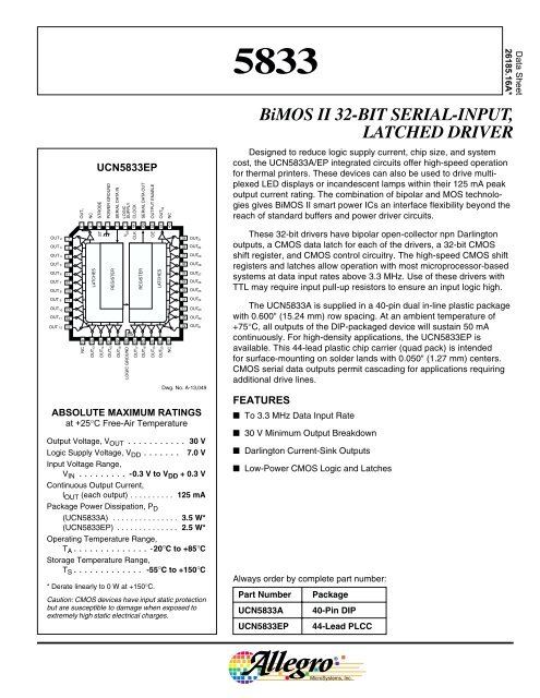
UCN<strong>5833</strong>EP<br />
SERIAL DATA IN<br />
LOGIC<br />
SUPPLY<br />
CLOCK<br />
SERIAL DATA OUT<br />
NC 18<br />
6<br />
OUT 19<br />
5<br />
13<br />
LATCHES<br />
20<br />
4<br />
OUT ST<br />
14<br />
21<br />
3<br />
OUT15 REGISTER<br />
22<br />
2<br />
OUT16 23<br />
1<br />
LOGIC GROUND<br />
VDD 24<br />
44<br />
OUT CLK<br />
17<br />
REGISTER<br />
OUT18 25<br />
43<br />
OUT 26<br />
19<br />
OE 42<br />
OUT 27<br />
LATCHES<br />
20<br />
41<br />
NC 28 40<br />
ABSOLUTE MAXIMUM RATINGS<br />
at +25°C Free-Air Temperature<br />
Output Voltage, V OUT . . . . . . . . . . . 30 V<br />
Logic Supply Voltage, V DD . . . . . . . 7.0 V<br />
Input Voltage Range,<br />
V IN . . . . . . . . . -0.3 V to V DD + 0.3 V<br />
Continuous Output Current,<br />
l OUT (each output) . . . . . . . . . . 125 mA<br />
Package Power Dissipation, P D<br />
(UCN<strong>5833</strong>A) . . . . . . . . . . . . . . . 3.5 W*<br />
(UCN<strong>5833</strong>EP) . . . . . . . . . . . . . . 2.5 W*<br />
Operating Temperature Range,<br />
T A . . . . . . . . . . . . . . -20°C to +85°C<br />
Storage Temperature Range,<br />
T S . . . . . . . . . . . . . -55°C to +150°C<br />
* Derate linearly to 0 W at +150°C.<br />
Dwg. No. A-13,049<br />
Caution: CMOS devices have input static protection<br />
but are susceptible to damage when exposed to<br />
extremely <strong>high</strong> static electrical charges.<br />
SUB<br />
OUTPUT ENABLE<br />
OUT <strong>32</strong><br />
NC<br />
39 OUT31 38 OUT30 37 OUT29 36 OUT28 35 OUT27 34 OUT26 33 OUT25 <strong>32</strong> OUT24 31 OUT23 30 OUT22 29 OUT21 <strong>5833</strong><br />
BiMOS II <strong>32</strong>-BIT SERIAL-INPUT,<br />
LATCHED DRIVER<br />
Designed to reduce logic supply current, chip size, and system<br />
cost, the UCN<strong>5833</strong>A/EP integrated circuits offer <strong>high</strong>-speed operation<br />
for thermal printers. These devices can also be used to drive multiplexed<br />
LED displays or incandescent lamps within their 125 mA peak<br />
output current rating. The combination of bipolar and MOS technologies<br />
gives BiMOS II smart power ICs an interface flexibility beyond the<br />
reach of standard buffers and power driver circuits.<br />
These <strong>32</strong>-<strong>bit</strong> drivers have bipolar open-collector npn Darlington<br />
<strong>outputs</strong>, a CMOS data latch for each of the drivers, a <strong>32</strong>-<strong>bit</strong> CMOS<br />
<strong>shift</strong> <strong>register</strong>, and CMOS control circuitry. The <strong>high</strong>-speed CMOS <strong>shift</strong><br />
<strong>register</strong>s and latches allow operation with most microprocessor-based<br />
systems at data input rates above 3.3 MHz. Use of these drivers with<br />
TTL may require input pull-up resistors to ensure an input logic <strong>high</strong>.<br />
The UCN<strong>5833</strong>A is supplied in a 40-pin dual in-line plastic package<br />
with 0.600" (15.24 mm) row spacing. At an ambient temperature of<br />
+75°C, all <strong>outputs</strong> of the DlP-packaged device will sustain 50 mA<br />
continuously. For <strong>high</strong>-density applications, the UCN<strong>5833</strong>EP is<br />
available. This 44-lead plastic chip carrier (quad pack) is intended<br />
for surface-mounting on solder lands with 0.050" (1.27 mm) centers.<br />
CMOS serial data <strong>outputs</strong> permit cascading for applications requiring<br />
additional drive lines.<br />
FEATURES<br />
■ To 3.3 MHz Data Input Rate<br />
■ 30 V Minimum Output Breakdown<br />
■ Darlington Current-Sink Outputs<br />
■ Low-Power CMOS Logic and Latches<br />
Always order by complete part number:<br />
Part Number Package<br />
UCN<strong>5833</strong>A 40-Pin DIP<br />
UCN<strong>5833</strong>EP 44-Lead PLCC<br />
Data Sheet<br />
26185.16A*
<strong>5833</strong><br />
BiMOS II <strong>32</strong>-BIT<br />
SERIAL-INPUT,<br />
LATCHED DRIVER<br />
LOGIC<br />
SUPPLY<br />
SERIAL<br />
DATA IN<br />
2<br />
POWER<br />
GROUND<br />
3<br />
STROBE 4<br />
OUT<br />
1<br />
OUT<br />
2<br />
OUT<br />
3<br />
OUT<br />
4<br />
OUT<br />
5<br />
OUT<br />
6<br />
OUT 7<br />
OUT 8<br />
OUT 9<br />
OUT 10<br />
OUT 11<br />
OUT 12<br />
1<br />
5<br />
6<br />
7<br />
8<br />
9<br />
10<br />
11<br />
12<br />
12<br />
14<br />
15<br />
16<br />
OUT<br />
13<br />
17<br />
OUT<br />
14 18<br />
OUT<br />
15 19<br />
OUT<br />
16 20<br />
V CLK<br />
DD<br />
ST<br />
LATCHES<br />
UCN<strong>5833</strong>A<br />
REGISTER<br />
REGISTER<br />
LATCHES<br />
OE<br />
SUB<br />
40<br />
LOGIC CLOCK<br />
SUPPLY<br />
39 SERIAL<br />
DATA OUT<br />
38 OUTPUT<br />
ENABLE<br />
37 OUT<br />
<strong>32</strong><br />
36<br />
35<br />
34<br />
33<br />
<strong>32</strong><br />
31<br />
30<br />
29<br />
28<br />
27<br />
26<br />
25<br />
24<br />
23<br />
22<br />
21<br />
OUT 31<br />
OUT 30<br />
OUT 29<br />
OUT 28<br />
OUT 27<br />
OUT 26<br />
OUT 25<br />
OUT 24<br />
OUT 23<br />
OUT 22<br />
OUT 21<br />
OUT 20<br />
OUT 19<br />
OUT 18<br />
OUT 17<br />
LOGIC<br />
GROUND<br />
Dwg. No. A-13,048<br />
CLOCK<br />
SERIAL<br />
DATA IN<br />
STROBE<br />
OUTPUT<br />
ENABLE<br />
FUNCTIONAL BLOCK DIAGRAM<br />
<strong>32</strong>-BIT SHIFT REGISTER<br />
LATCHES<br />
TYPICAL INPUT CIRCUIT<br />
IN<br />
OUT1 OUT2 OUT3 POWER OUT30 OUT31 OUT<strong>32</strong><br />
GROUND<br />
SUB<br />
TYPICAL OUTPUT DRIVER<br />
115 Northeast Cutoff, Box 15036<br />
115<br />
Worcester,<br />
Northeast<br />
Massachusetts<br />
Cutoff, Box 15036<br />
01615-0036 (508) 853-5000<br />
Worcester, Massachusetts 01615-0036 (508) 853-5000<br />
Copyright © 1986, 1995, Allegro MicroSystems, Inc.<br />
V DD<br />
V DD<br />
SERIAL DATA<br />
OUT<br />
SUB<br />
MOS<br />
BIPOLAR<br />
Dwg. No. A-13,050<br />
Dwg. No. A-13,051<br />
LOGIC<br />
GROUND<br />
Dwg. No. A-13,057<br />
OUT
TRUTH TABLE<br />
<strong>5833</strong><br />
BiMOS II <strong>32</strong>-BIT<br />
SERIAL-INPUT,<br />
LATCHED DRIVER<br />
ELECTRICAL CHARACTERISTICS at T A = +25°C, V DD = 5 V (unless otherwise noted).<br />
Limits<br />
Characteristic Symbol Test Conditions Min. Max. Units<br />
Output Leakage Current I CEX<br />
Collector-Emitter V<br />
CE(SAT)<br />
Saturation Voltage<br />
Input Voltage V IN(1)<br />
V IN(0)<br />
Input Current l IN(1)<br />
l IN(0)<br />
Serial Output Voltage V OUT(1)<br />
V OUT(0)<br />
Supply Current l DD<br />
Serial Shift Register Contents Serial Latch Contents Output Output Contents<br />
Data Clock Data Strobe Enable<br />
Input Input I 1 I 2 I 3 ... I N-1 I N Output Input I 1 I 2 I 3 ... I N-1 I N Input I 1 I 2 I 3 ... I N-1 I N<br />
H H R 1 R 2 ... R N-2 R N-1 R N-1<br />
L L R 1 R 2 ... R N-2 R N-1 R N-1<br />
X R 1 R 2 R 3 ... R N-1 R N R N<br />
X X X ... X X X L R 1 R 2 R 3 ... R N-1 R N<br />
P 1 P 2 P 3 ... P N-1 P N P N H P 1 P 2 P 3 ... P N-1 P N H P 1 P 2 P 3 ... P N-1 P N<br />
L = Low Logic Level H = High Logic Level X = Irrelevant P = Present State R = Previous State<br />
V OUT = 30 V, T A = 70°C — 10 µA<br />
l OUT = 50 mA — 1.2 V<br />
l OUT = 100 mA — 1.7 V<br />
3.5 5.3 V<br />
-0.3 +0.8 V<br />
V IN = 5.0 V — 1.0 µA<br />
V IN = 0 V — -1.0 µA<br />
I OUT = -200 µA 4.5 — V<br />
I OUT = 200 µA — 0.3 V<br />
One output ON, l OUT = 100 mA — 1.0 mA<br />
All <strong>outputs</strong> OFF — 50 µA<br />
Output Rise Time t<br />
r<br />
l = 100 mA, 10% to 90%<br />
OUT<br />
— 500 ns<br />
Output Fall Time t<br />
f<br />
l = 100 mA, 90% to 10%<br />
OUT<br />
— 500 ns<br />
NOTE: Positive (negative) current is defined as going into (coming out of) the specified device pin.<br />
X X X ... X X L H H H ... H H
<strong>5833</strong><br />
BiMOS II <strong>32</strong>-BIT<br />
SERIAL-INPUT,<br />
LATCHED DRIVER<br />
CLOCK<br />
DATA IN<br />
STROBE<br />
OUTPUT<br />
ENABLE<br />
OUT<br />
N<br />
A D<br />
B<br />
C<br />
E F<br />
TIMING CONDITIONS<br />
(V DD = 5.0 V, Logic Levels are V DD and Ground)<br />
A. Minimum Data Active Time Before Clock Pulse<br />
(Data Set-Up Time) .......................................................................... 75 ns<br />
B. Minimum Data Active Time After Clock Pulse<br />
(Data Hold Time) ............................................................................. 75 ns<br />
C. Minimum Data Pulse Width ................................................................ 150 ns<br />
D. Minimum Clock Pulse Width ............................................................... 150 ns<br />
E. Minimum Time Between Clock Activation and Strobe ....................... 300 ns<br />
F. Minimum Strobe Pulse Width ............................................................. 100 ns<br />
G. Typical Time Between Strobe Activation and<br />
Output Transition ........................................................................... 500 ns<br />
115 Northeast Cutoff, Box 15036<br />
Worcester, Massachusetts 01615-0036 (508) 853-5000<br />
Dwg. No. A-12,276A<br />
Serial Data present at the input is transferred to the <strong>shift</strong> <strong>register</strong><br />
on the logic “0” to logic “1” transition of the CLOCK input pulse. On<br />
succeeding CLOCK pulses, the <strong>register</strong>s <strong>shift</strong> data information towards<br />
the SERIAL DATA OUTPUT. The SERIAL DATA must appear at the<br />
input prior to the rising edge of the CLOCK input waveform.<br />
Information present at any <strong>register</strong> is transferred to its respective<br />
latch when the STROBE is <strong>high</strong> (serial-to-parallel conversion). The<br />
latches will continue to accept new data as long as the STROBE is<br />
held <strong>high</strong>. Applications where the latches are bypassed (STROBE tied<br />
<strong>high</strong>) will require that the OUTPUT ENABLE input be low during serial<br />
data entry.<br />
When the OUTPUT ENABLE input is low, all of the output buffers<br />
are disabled (OFF) without affecting the information stored in the<br />
latches or <strong>shift</strong> <strong>register</strong>. With the OUTPUT ENABLE input <strong>high</strong>, the<br />
<strong>outputs</strong> are controlled by the state of the latches.<br />
G
0.580<br />
0.485<br />
0.250<br />
MAX<br />
14.73<br />
12.<strong>32</strong><br />
6.35<br />
MAX<br />
0.015<br />
MIN<br />
0.39<br />
MIN<br />
40<br />
1 2<br />
0.070<br />
0.030<br />
3<br />
40<br />
0.022<br />
0.014<br />
1 2<br />
1.77<br />
0.77<br />
3<br />
0.558<br />
0.356<br />
UCN<strong>5833</strong>A<br />
Dimensions in Inches<br />
(controlling dimensions)<br />
Dimensions in Millimeters<br />
(for reference only)<br />
20<br />
2.54<br />
BSC<br />
NOTES: 1. Exact body and lead configuration at vendor’s option within limits shown.<br />
2. Lead spacing tolerance is non-cumulative.<br />
3. Lead thickness is measured at seating plane or below.<br />
4<br />
4<br />
2.095<br />
1.980<br />
53.2<br />
50.3<br />
21<br />
20<br />
0.100<br />
BSC<br />
21<br />
0.005<br />
MIN<br />
0.200<br />
0.115<br />
0.13<br />
MIN<br />
5.08<br />
2.93<br />
0.015<br />
0.008<br />
0.381<br />
0.204<br />
<strong>5833</strong><br />
BiMOS II <strong>32</strong>-BIT<br />
SERIAL-INPUT,<br />
LATCHED DRIVER<br />
0.700<br />
MAX<br />
0.600<br />
BSC<br />
Dwg. MA-003-40 in<br />
17.78<br />
MAX<br />
15.24<br />
BSC<br />
Dwg. MA-003-40 mm
<strong>5833</strong><br />
BiMOS II <strong>32</strong>-BIT<br />
SERIAL-INPUT,<br />
LATCHED DRIVER<br />
0.319<br />
0.291<br />
8.10<br />
7.39<br />
8.10<br />
7.39<br />
0.021<br />
0.013<br />
0.319<br />
0.291<br />
0.050<br />
BSC<br />
0.533<br />
0.331<br />
1.27<br />
BSC<br />
0.020<br />
MIN<br />
0.180<br />
0.165<br />
0.51<br />
MIN<br />
4.57<br />
4.20<br />
0.695<br />
0.685<br />
0.656<br />
0.650<br />
17.65<br />
17.40<br />
16.662<br />
16.510<br />
UCN<strong>5833</strong>EP<br />
Dimensions in Inches<br />
(controlling dimensions)<br />
29<br />
0.0<strong>32</strong><br />
0.026<br />
39<br />
Dimensions in Millimeters<br />
(for reference only)<br />
29<br />
0.812<br />
0.661<br />
39<br />
28<br />
40<br />
28<br />
44<br />
1<br />
0.656<br />
0.650<br />
40 44 1 2<br />
6<br />
16.662<br />
16.510<br />
17.65<br />
17.40<br />
NOTES: 1. Exact body and lead configuration at vendor’s option within limits shown.<br />
2. Lead spacing tolerance is non-cumulative.<br />
0.695<br />
0.685<br />
INDEX AREA<br />
INDEX AREA<br />
Dwg. MA-005-44A mm<br />
115 Northeast Cutoff, Box 15036<br />
Worcester, Massachusetts 01615-0036 (508) 853-5000<br />
18<br />
2 6<br />
18<br />
17<br />
7<br />
Dwg. MA-005-44A in<br />
17<br />
7
<strong>5833</strong><br />
BiMOS II <strong>32</strong>-BIT<br />
SERIAL-INPUT,<br />
LATCHED DRIVER<br />
The products described here are manufactured under one or more<br />
U.S. patents or U.S. patents pending.<br />
Allegro MicroSystems, Inc. reserves the right to make, from time to<br />
time, such departures from the detail specifications as may be required<br />
to permit improvements in the performance, reliability, or<br />
manufacturability of its products. Before placing an order, the user is<br />
cautioned to verify that the information being relied upon is current.<br />
Allegro products are not authorized for use as critical components<br />
in life-support devices or systems without express written approval.<br />
The information included herein is believed to be accurate and<br />
reliable. However, Allegro MicroSystems, Inc. assumes no responsibility<br />
for its use; nor for any infringement of patents or other rights of<br />
third parties which may result from its use.
<strong>5833</strong><br />
BiMOS II <strong>32</strong>-BIT<br />
SERIAL-INPUT,<br />
LATCHED DRIVER<br />
115 Northeast Cutoff, Box 15036<br />
Worcester, Massachusetts 01615-0036 (508) 853-5000<br />
POWER<br />
INTERFACE DRIVERS<br />
Function Output Ratings* Part Number †<br />
SERIAL-INPUT LATCHED DRIVERS<br />
8-Bit (saturated drivers) -120 mA 50 V‡ 5895<br />
8-Bit 350 mA 50 V 5821<br />
8-Bit 350 mA 80 V 5822<br />
8-Bit 350 mA 50 V‡ 5841<br />
8-Bit 350 mA 80 V‡ 5842<br />
8-Bit (constant-current LED driver) 75 mA 17 V 6275<br />
8-Bit (DMOS drivers) 250 mA 50 V 6595<br />
8-Bit (DMOS drivers) 350 mA 50 V‡ 6A595<br />
8-Bit (DMOS drivers) 100 mA 50 V 6B595<br />
10-Bit (active pull-downs) -25 mA 60 V 5810-F and 6809/10<br />
12-Bit (active pull-downs) -25 mA 60 V 5811 and 6811<br />
16-Bit (constant-current LED driver) 75 mA 17 V 6276<br />
20-Bit (active pull-downs) -25 mA 60 V 5812-F and 6812<br />
<strong>32</strong>-Bit (active pull-downs) -25 mA 60 V 5818-F and 6818<br />
<strong>32</strong>-Bit 100 mA 30 V <strong>5833</strong><br />
<strong>32</strong>-Bit (saturated drivers) 100 mA 40 V 58<strong>32</strong><br />
PARALLEL-INPUT LATCHED DRIVERS<br />
4-Bit 350 mA 50 V‡ 5800<br />
8-Bit -25 mA 60 V 5815<br />
8-Bit 350 mA 50 V‡ 5801<br />
8-Bit (DMOS drivers) 100 mA 50 V 6B273<br />
8-Bit (DMOS drivers) 250 mA 50 V 6273<br />
SPECIAL-PURPOSE DEVICES<br />
Unipolar Stepper Motor Translator/Driver 1.25 A 50 V‡ 5804<br />
Addressable 8-Bit Decoder/DMOS Driver 250 mA 50 V 6259<br />
Addressable 8-Bit Decoder/DMOS Driver 350 mA 50 V‡ 6A259<br />
Addressable 8-Bit Decoder/DMOS Driver 100 mA 50 V 6B259<br />
Addressable 28-Line Decoder/Driver 450 mA 30 V 6817<br />
* Current is maximum specified test condition, <strong>voltage</strong> is maximum rating. See specification for sustaining <strong>voltage</strong> limits.<br />
Negative current is defined as coming out of (sourcing) the output.<br />
† Complete part number includes additional characters to indicate operating temperature range and package style.<br />
‡ Internal transient-suppression diodes included for inductive-load protection.