

MPC5642A - Freescale Semiconductor
MPC5642A - Freescale Semiconductor
MPC5642A - Freescale Semiconductor

You also want an ePaper? Increase the reach of your titles
YUMPU automatically turns print PDFs into web optimized ePapers that Google loves.
<strong>Freescale</strong> <strong>Semiconductor</strong><br />
Data Sheet: Technical Data<br />
Qorivva <strong>MPC5642A</strong><br />
Microcontroller Data Sheet<br />
• 150 MHz e200z4 Power Architecture core<br />
– Variable length instruction encoding (VLE)<br />
– Superscalar architecture with 2 execution units<br />
– Up to 2 integer or floating point instructions per cycle<br />
– Up to 4 multiply and accumulate operations per cycle<br />
• Memory organization<br />
– 2 MB on-chip flash memory with ECC and<br />
read-while-write (RWW)<br />
– 128 KB on-chip SRAM with standby functionality (32<br />
KB) and ECC<br />
– 8 KB instruction cache (with line locking), configurable<br />
as 2- or 4-way<br />
– 14 + 3 KB eTPU code and data RAM<br />
– 4 4 crossbar switch (XBAR)<br />
– 24-entry MMU<br />
• Fail Safe Protection<br />
– 16-entry Memory Protection Unit (MPU)<br />
– CRC unit with 3 submodules<br />
– Junction temperature sensor<br />
• Interrupt<br />
– Configurable interrupt controller (INTC) with<br />
non-maskable interrupt (NMI)<br />
– 64-channel eDMA<br />
• Serial channels<br />
– 3 eSCI modules<br />
– 3 DSPI modules (2 of which support downstream Micro<br />
Second Channel [MSC])<br />
– 3 FlexCAN modules with 64 message buffers each<br />
– 1 FlexRay module (V2.1) up to 10 Mbit/s w/dual or<br />
single channel, 128 message objects, ECC<br />
• 1 eMIOS<br />
– 24 unified channels<br />
• 1 eTPU2 (second generation eTPU)<br />
—32 standard channels<br />
© <strong>Freescale</strong> <strong>Semiconductor</strong>, Inc., 2009, 2010, 2012. All rights reserved.<br />
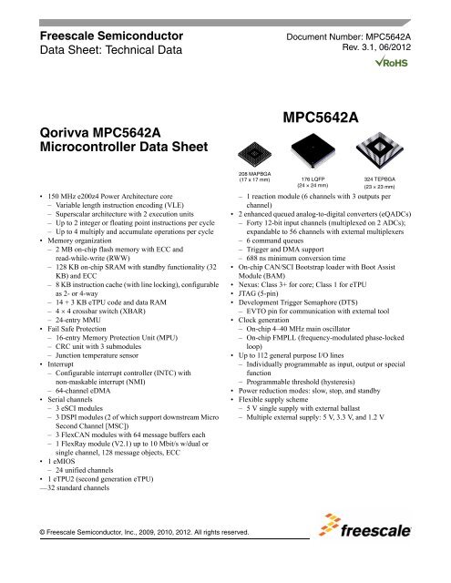
208 MAPBGA<br />
(17 x 17 mm)<br />
Document Number: <strong>MPC5642A</strong><br />
Rev. 3.1, 06/2012<br />
<strong>MPC5642A</strong><br />
176 LQFP 324 TEPBGA<br />
(24 × 24 mm) (23 × 23 mm)<br />
– 1 reaction module (6 channels with 3 outputs per<br />
channel)<br />
• 2 enhanced queued analog-to-digital converters (eQADCs)<br />
– Forty 12-bit input channels (multiplexed on 2 ADCs);<br />
expandable to 56 channels with external multiplexers<br />
– 6 command queues<br />
– Trigger and DMA support<br />
– 688 ns minimum conversion time<br />
• On-chip CAN/SCI Bootstrap loader with Boot Assist<br />
Module (BAM)<br />
• Nexus: Class 3+ for core; Class 1 for eTPU<br />
• JTAG (5-pin)<br />
• Development Trigger Semaphore (DTS)<br />
– EVTO pin for communication with external tool<br />
• Clock generation<br />
– On-chip 4–40 MHz main oscillator<br />
– On-chip FMPLL (frequency-modulated phase-locked<br />
loop)<br />
• Up to 112 general purpose I/O lines<br />
– Individually programmable as input, output or special<br />
function<br />
– Programmable threshold (hysteresis)<br />
• Power reduction modes: slow, stop, and standby<br />
• Flexible supply scheme<br />
– 5 V single supply with external ballast<br />
– Multiple external supply: 5 V, 3.3 V, and 1.2 V
1 Introduction. . . . . . . . . . . . . . . . . . . . . . . . . . . . . . . . . . . . . . . .3<br />
1.1 Document overview. . . . . . . . . . . . . . . . . . . . . . . . . . . . .3<br />
1.2 Description . . . . . . . . . . . . . . . . . . . . . . . . . . . . . . . . . . .3<br />
1.3 Device feature summary . . . . . . . . . . . . . . . . . . . . . . . . .3<br />
1.4 Block diagram . . . . . . . . . . . . . . . . . . . . . . . . . . . . . . . . .5<br />
1.5 Feature details . . . . . . . . . . . . . . . . . . . . . . . . . . . . . . . .9<br />
1.5.1 e200z4 core. . . . . . . . . . . . . . . . . . . . . . . . . . . . .9<br />
1.5.2 Crossbar switch (XBAR) . . . . . . . . . . . . . . . . . .10<br />
1.5.3 Enhanced direct memory access (eDMA) . . . . .10<br />
1.5.4 Interrupt controller (INTC) . . . . . . . . . . . . . . . . .11<br />
1.5.5 Memory protection unit (MPU). . . . . . . . . . . . . .11<br />
1.5.6 Frequency-modulated phase-locked loop<br />
(FMPLL). . . . . . . . . . . . . . . . . . . . . . . . . . . . . . .12<br />
1.5.7 System integration unit (SIU). . . . . . . . . . . . . . .12<br />
1.5.8 Flash memory . . . . . . . . . . . . . . . . . . . . . . . . . .13<br />
1.5.9 Static random access memory (SRAM) . . . . . .14<br />
1.5.10 Boot assist module (BAM) . . . . . . . . . . . . . . . . .14<br />
1.5.11 Enhanced modular input/output system<br />
(eMIOS) . . . . . . . . . . . . . . . . . . . . . . . . . . . . . . .14<br />
1.5.12 Second generation enhanced time processing<br />
unit (eTPU2) . . . . . . . . . . . . . . . . . . . . . . . . . . .15<br />
1.5.13 Reaction module (REACM) . . . . . . . . . . . . . . . .16<br />
1.5.14 Enhanced queued analog-to-digital converter<br />
(eQADC) . . . . . . . . . . . . . . . . . . . . . . . . . . . . . .17<br />
1.5.15 Deserial serial peripheral interface (DSPI) . . . .18<br />
1.5.16 Enhanced serial communications interface<br />
(eSCI) . . . . . . . . . . . . . . . . . . . . . . . . . . . . . . . .19<br />
1.5.17 Controller area network (FlexCAN) . . . . . . . . . .19<br />
1.5.18 FlexRay . . . . . . . . . . . . . . . . . . . . . . . . . . . . . . .20<br />
1.5.19 System timers . . . . . . . . . . . . . . . . . . . . . . . . . .20<br />
1.5.20 Software watchdog timer (SWT) . . . . . . . . . . . .21<br />
1.5.21 Cyclic redundancy check (CRC) module . . . . . .21<br />
1.5.22 Error correction status module (ECSM). . . . . . .22<br />
1.5.23 Peripheral bridge (PBRIDGE) . . . . . . . . . . . . . .22<br />
1.5.24 Calibration bus interface . . . . . . . . . . . . . . . . . .22<br />
1.5.25 Power management controller (PMC) . . . . . . . .22<br />
1.5.26 Nexus port controller (NPC) . . . . . . . . . . . . . . .23<br />
1.5.27 JTAG controller (JTAGC) . . . . . . . . . . . . . . . . . .23<br />
1.5.28 Development trigger semaphore (DTS). . . . . . .23<br />
2 Pinout and signal description . . . . . . . . . . . . . . . . . . . . . . . . .23<br />
2.1 176 LQFP pinout. . . . . . . . . . . . . . . . . . . . . . . . . . . . . .24<br />
2.2 208 MAP BGA ballmap . . . . . . . . . . . . . . . . . . . . . . . . .25<br />
2.3 324 TEPBGA ballmap. . . . . . . . . . . . . . . . . . . . . . . . . .26<br />
2.4 Signal summary . . . . . . . . . . . . . . . . . . . . . . . . . . . . . .30<br />
2<br />
Table of Contents<br />
<strong>MPC5642A</strong> Microcontroller Data Sheet, Rev. 3.1<br />
2.5 Signal details . . . . . . . . . . . . . . . . . . . . . . . . . . . . . . . . 49<br />
3 Electrical characteristics . . . . . . . . . . . . . . . . . . . . . . . . . . . . 55<br />
3.1 Parameter classification. . . . . . . . . . . . . . . . . . . . . . . . 55<br />
3.2 Maximum ratings . . . . . . . . . . . . . . . . . . . . . . . . . . . . . 56<br />
3.3 Thermal characteristics . . . . . . . . . . . . . . . . . . . . . . . . 58<br />
3.3.1 General notes for specifications at maximum<br />
junction temperature . . . . . . . . . . . . . . . . . . . . . . . . . . 59<br />
3.4 EMI (electromagnetic interference) characteristics . . . 61<br />
3.5 Electrostatic discharge (ESD) characteristics . . . . . . . 62<br />
3.6 Power management control (PMC) and power on<br />
reset (POR) electrical specifications . . . . . . . . . . . . . . 62<br />
3.6.1 Regulator example . . . . . . . . . . . . . . . . . . . . . . 65<br />
3.6.2 Recommended power transistors. . . . . . . . . . . 66<br />
3.7 Power up/down sequencing. . . . . . . . . . . . . . . . . . . . . 66<br />
3.8 DC electrical specifications . . . . . . . . . . . . . . . . . . . . . 67<br />
3.9 I/O pad current specifications . . . . . . . . . . . . . . . . . . . 72<br />
3.9.1 I/O pad V RC33 current specifications . . . . . . . . 73<br />
3.9.2 LVDS pad specifications. . . . . . . . . . . . . . . . . . 74<br />
3.10 Oscillator and PLLMRFM electrical characteristics . . . 75<br />
3.11 Temperature sensor electrical characteristics . . . . . . . 77<br />
3.12 eQADC electrical characteristics. . . . . . . . . . . . . . . . . 77<br />
3.13 Configuring SRAM wait states. . . . . . . . . . . . . . . . . . . 79<br />
3.14 Platform flash controller electrical characteristics . . . . 80<br />
3.15 Flash memory electrical characteristics . . . . . . . . . . . 80<br />
3.16 AC specifications . . . . . . . . . . . . . . . . . . . . . . . . . . . . . 82<br />
3.16.1 Pad AC specifications. . . . . . . . . . . . . . . . . . . . 82<br />
3.17 AC timing . . . . . . . . . . . . . . . . . . . . . . . . . . . . . . . . . . . 86<br />
3.17.1 Reset and configuration pin timing. . . . . . . . . . 86<br />
3.17.2 IEEE 1149.1 interface timing . . . . . . . . . . . . . . 86<br />
3.17.3 Nexus timing. . . . . . . . . . . . . . . . . . . . . . . . . . . 90<br />
3.17.4 Calibration bus interface timing . . . . . . . . . . . . 95<br />
3.17.5 External interrupt timing (IRQ pin) . . . . . . . . . . 99<br />
3.17.6 eTPU timing . . . . . . . . . . . . . . . . . . . . . . . . . . . 99<br />
3.17.7 eMIOS timing . . . . . . . . . . . . . . . . . . . . . . . . . 100<br />
3.17.8 DSPI timing . . . . . . . . . . . . . . . . . . . . . . . . . . 100<br />
3.17.9 eQADC SSI timing . . . . . . . . . . . . . . . . . . . . . 107<br />
3.17.10FlexCAN system clock source . . . . . . . . . . . . 108<br />
4 Packages. . . . . . . . . . . . . . . . . . . . . . . . . . . . . . . . . . . . . . . 109<br />
4.1 Package mechanical data . . . . . . . . . . . . . . . . . . . . . 109<br />
4.1.1 176 LQFP. . . . . . . . . . . . . . . . . . . . . . . . . . . . 109<br />
4.1.2 208 MAPBGA. . . . . . . . . . . . . . . . . . . . . . . . . 112<br />
4.1.3 324 TEPBGA . . . . . . . . . . . . . . . . . . . . . . . . . 114<br />
5 Ordering information . . . . . . . . . . . . . . . . . . . . . . . . . . . . . . 116<br />
6 Document revision history. . . . . . . . . . . . . . . . . . . . . . . . . . 117<br />
<strong>Freescale</strong> <strong>Semiconductor</strong>
1 Introduction<br />
1.1 Document overview<br />
This document provides electrical specifications, pin assignments, and package diagrams for the <strong>MPC5642A</strong> series of<br />
microcontroller units (MCUs). It also describes the device features and highlights important electrical and physical<br />
characteristics. For functional characteristics, refer to the device reference manual.<br />
1.2 Description<br />
<strong>MPC5642A</strong> Microcontroller Data Sheet, Rev. 3.1<br />
Introduction<br />
This microcontroller is a 32-bit system-on-chip (SoC) device intended for use in mid-range engine control and automotive<br />
transmission control applications.<br />
It is compatible with devices in <strong>Freescale</strong>’s MPC5600 family and offers performance and capabilities beyond the MPC5632M<br />
devices.<br />
The microcontroller’s e200z4 host processor core is built on the Power Architecture ® technology and designed specifically for<br />
embedded applications. In addition to the Power Architecture technology, this core supports instructions for digital signal<br />
processing (DSP).<br />
The device has two levels of memory hierarchy consisting of 8 KB of instruction cache, backed by a 128 KB on-chip SRAM<br />
and a 2 MB internal flash memory.<br />
For development, the device includes a calibration bus that is accessible only when using the <strong>Freescale</strong> VertiCal Calibration<br />
System.<br />
1.3 Device feature summary<br />
Table 1 summarizes the <strong>MPC5642A</strong> features and compares them to those of the MPC5644A.<br />
Table 1. <strong>MPC5642A</strong> device feature summary<br />
Feature <strong>MPC5642A</strong> MPC5644A<br />
Process 90 nm<br />
Core e200z4<br />
SIMD Yes<br />
VLE Yes<br />
Cache 8 KB instruction<br />
Non-Maskable Interrupt (NMI) NMI and Critical Interrupt<br />
MMU 24-entry<br />
MPU 16-entry<br />
Crossbar switch 4 4 5 4<br />
Core performance 0–150 MHz<br />
Windowing software watchdog Yes<br />
Core Nexus Class 3+<br />
SRAM 128 KB 192 KB<br />
Flash 2 MB 4 MB<br />
Flash fetch accelerator 4 128-bit 4 256-bit<br />
<strong>Freescale</strong> <strong>Semiconductor</strong> 3
Introduction<br />
Table 1. <strong>MPC5642A</strong> device feature summary (continued)<br />
Feature <strong>MPC5642A</strong> MPC5644A<br />
External bus None 16-bit (incl. 32-bit muxed)<br />
Calibration bus 16-bit (incl. 32-bit muxed)<br />
DMA 64 channels<br />
DMA Nexus None<br />
Serial 3<br />
eSCI_A Yes (MSC uplink)<br />
eSCI_B Yes (MSC uplink)<br />
eSCI_C Yes<br />
CAN 3<br />
CAN_A 64 message buffers<br />
CAN_B 64 message buffers<br />
CAN_C 64 message buffers<br />
SPI 3<br />
Micro Second Channel (MSC) bus downlink Yes<br />
DSPI_A No<br />
DSPI_B Yes (with LVDS)<br />
DSPI_C Yes (with LVDS)<br />
DSPI_D Yes<br />
FlexRay Yes<br />
System timers 5 PIT channels<br />
4 STM channels<br />
1 Software Watchdog<br />
eMIOS 24 channels<br />
eTPU 32-channel eTPU2<br />
Code memory 14 KB<br />
Data memory 3 KB<br />
Reaction module 6 channels<br />
Interrupt controller 485 channels 1<br />
ADC 40 channels<br />
ADC_0 Yes<br />
ADC_1 Yes<br />
Temperature sensor Yes<br />
Variable gain amplifier Yes<br />
Decimation filter 2<br />
Sensor diagnostics Yes<br />
<strong>MPC5642A</strong> Microcontroller Data Sheet, Rev. 3.1<br />
4 <strong>Freescale</strong> <strong>Semiconductor</strong>
CRC Yes<br />
FMPLL Yes<br />
VRC Yes<br />
Supplies 5 V, 3.3 V 2<br />
1.4 Block diagram<br />
Table 1. <strong>MPC5642A</strong> device feature summary (continued)<br />
Feature <strong>MPC5642A</strong> MPC5644A<br />
Low-power modes Stop mode<br />
Slow mode<br />
Packages 176 LQFP 3<br />
208 MAPBGA 3,4<br />
324 TEPBGA 5<br />
496-pin CSP 6<br />
1<br />
197 interrupt vectors are reserved.<br />
2<br />
5 V single supply only for 176 LQFP<br />
3<br />
Pinout compatible with <strong>Freescale</strong>’s MPC5634M devices<br />
Figure 1 shows a top-level block diagram of the <strong>MPC5642A</strong> series.<br />
<strong>MPC5642A</strong> Microcontroller Data Sheet, Rev. 3.1<br />
176 LQFP 3<br />
208 MAPBGA 3,4<br />
324 TEPBGA 5<br />
496-pin CSP 6<br />
Introduction<br />
4<br />
Pinout compatible with <strong>Freescale</strong>’s MPC5534<br />
5 Ballmap upwardly compatible with the standardized package ballmap used for various <strong>Freescale</strong> MPC563xM family<br />
members<br />
6 For <strong>Freescale</strong> VertiCal Calibration System only<br />
<strong>Freescale</strong> <strong>Semiconductor</strong> 5
Introduction<br />
eMIOS<br />
24<br />
Channel<br />
2 MB<br />
Flash<br />
Interrupt<br />
Controller<br />
64-channel<br />
eDMA<br />
S0<br />
3 KB Data<br />
RAM<br />
14 KB Code<br />
RAM<br />
128 KB<br />
SRAM<br />
eTPU2<br />
32<br />
Channel<br />
Power Architecture<br />
e200z4<br />
SPE<br />
VLE<br />
MMU<br />
8 KB I-cache<br />
Crossbar Switch<br />
MPU<br />
S2 S7<br />
ADC – Analog to Digital Converter<br />
ADCi – ADC interface<br />
AMux – Analog Multiplexer<br />
BAM – Boot Assist Module<br />
CRC – Cyclic Redundancy Check unit<br />
DEC – Decimation Filter<br />
DTS – Development Trigger Semaphore<br />
DSPI – Deserial/Serial Peripheral Interface<br />
ECSM – Error Correction Status Module<br />
eDMA – Enhanced Direct Memory Access<br />
eMIOS – Enhanced Modular Input Output System<br />
eSCI – Enhanced Serial Communications Interface<br />
eTPU2 – Second gen. Enhanced Time Processing Unit<br />
FlexCAN – Controller Area Network<br />
FMPLL – Frequency-Modulated Phase-Locked Loop<br />
LEGEND<br />
JTAG – IEEE 1149.1 Test Controller<br />
MMU – Memory Management Unit<br />
MPU – Memory Protection Unit<br />
PMC – Power Management Controller<br />
PIT – Periodic Interrupt Timer<br />
RCOSC – Low-speed RC Oscillator<br />
REACM – Reaction Module<br />
SIU – System Integration Unit<br />
SPE – Signal Processing Extension<br />
SRAM – Static RAM<br />
STM – System Timer Module<br />
SWT – Software Watchdog Timer<br />
VGA – Variable Gain Amplifier<br />
VLE – Variable Length (instruction) Encoding<br />
XOSC – XTAL Oscillator<br />
Figure 1. <strong>MPC5642A</strong> series block diagram<br />
Table 2 summarizes the functions of the blocks present on the <strong>MPC5642A</strong> series microcontrollers.<br />
<strong>MPC5642A</strong> Microcontroller Data Sheet, Rev. 3.1<br />
6 <strong>Freescale</strong> <strong>Semiconductor</strong><br />
JTAG<br />
Nexus<br />
IEEE-ISTO<br />
5001-2010<br />
FlexRay<br />
M4 M0 M1<br />
M6<br />
REACM 6 ch<br />
DTS<br />
Analog PLL<br />
RCOSC<br />
XOSC<br />
I/O Bridge<br />
FMPLL<br />
CRC<br />
BAM<br />
PMC<br />
STM<br />
Debug<br />
S1<br />
Voltage Regulator<br />
Standby<br />
Regulator<br />
with Switch<br />
PIT<br />
SWT<br />
SIU<br />
FlexCAN x 3<br />
eSCI x 3<br />
ECSM<br />
DSPI x 3<br />
Temp Sens<br />
Calibration Bus Interface<br />
ADCi DEC<br />
x2<br />
ADC<br />
ADC<br />
VGA<br />
AMux
Table 2. <strong>MPC5642A</strong> series block summary<br />
Block Function<br />
Boot assist module (BAM) Block of read-only memory containing executable code that searches<br />
for user-supplied boot code and, if none is found, executes the BAM<br />
boot code resident in device ROM<br />
Calibration bus interface Transfers data across the crossbar switch to/from peripherals attached<br />
to the calibration system connector<br />
Controller area network (FlexCAN) Supports the standard CAN communications protocol<br />
Crossbar switch (XBAR) Internal busmaster<br />
Cyclic redundancy check (CRC) CRC checksum generator<br />
Deserial serial peripheral interface (DSPI) Provides a synchronous serial interface for communication with<br />
external devices<br />
e200z4 core Executes programs and interrupt handlers<br />
Enhanced direct memory access (eDMA) Performs complex data movements with minimal intervention from the<br />
core.<br />
Enhanced modular input-output system<br />
(eMIOS)<br />
Enhanced queued analog-to-digital<br />
converter (eQADC)<br />
Enhanced serial communication interface<br />
(eSCI)<br />
Provides the functionality to generate or measure events<br />
Provides accurate and fast conversions for a wide range of<br />
applications<br />
Provides asynchronous serial communication capability with<br />
peripheral devices and other microcontroller units<br />
Enhanced time processor unit (eTPU2) Second-generation co-processor processes real-time input events,<br />
performs output waveform generation, and accesses shared data<br />
without host intervention<br />
Error Correction Status Module (ECSM) The Error Correction Status Module supports a number of<br />
miscellaneous control functions for the platform, and includes registers<br />
for capturing information on platform memory errors if error-correcting<br />
codes (ECC) are implemented<br />
Flash memory Provides storage for program code, constants, and variables<br />
FlexRay Provides high-speed distributed control for advanced automotive<br />
applications<br />
Frequency-modulated phase-locked loop<br />
(FMPLL)<br />
Generates high-speed system clocks and supports programmable<br />
frequency modulation<br />
Interrupt controller (INTC) Provides priority-based preemptive scheduling of interrupt requests<br />
JTAG controller Provides the means to test chip functionality and connectivity while<br />
remaining transparent to system logic when not in test mode<br />
Memory protection unit (MPU) Provides hardware access control for all memory references<br />
generated<br />
Nexus port controller (NPC) Provides real-time development support capabilities in compliance<br />
with the IEEE-ISTO 5001-2010 standard<br />
Periodic interrupt timer (PIT) Produces periodic interrupts and triggers<br />
Reaction Module (REACM) Works in conjunction with the eQADC and eTPU2 to increase system<br />
performance by removing the CPU from the current control loop.<br />
<strong>MPC5642A</strong> Microcontroller Data Sheet, Rev. 3.1<br />
Introduction<br />
<strong>Freescale</strong> <strong>Semiconductor</strong> 7
Introduction<br />
Table 2. <strong>MPC5642A</strong> series block summary (continued)<br />
Block Function<br />
System Integration Unit (SIU) Controls MCU reset configuration, pad configuration, external<br />
interrupt, general purpose I/O (GPIO), internal peripheral multiplexing,<br />
and the system reset operation.<br />
Static random-access memory (SRAM) Provides storage for program code, constants, and variables<br />
System timers Includes periodic interrupt timer with real-time interrupt; output<br />
compare timer and system watchdog timer<br />
System watchdog timer (SWT) Provides protection from runaway code<br />
Temperature sensor Provides the temperature of the device as an analog value<br />
<strong>MPC5642A</strong> Microcontroller Data Sheet, Rev. 3.1<br />
8 <strong>Freescale</strong> <strong>Semiconductor</strong>
1.5 Feature details<br />
1.5.1 e200z4 core<br />
<strong>MPC5642A</strong> Microcontroller Data Sheet, Rev. 3.1<br />
Introduction<br />
<strong>MPC5642A</strong> devices have a high performance e200z4 core processor:<br />
• 32-bit Power Architecture technology programmer’s model<br />
• Variable Length Encoding (VLE) enhancements<br />
• Dual issue, 32-bit Power Architecture technology compliant CPU<br />
• 8 KB, 2/4-way set associative instruction cache<br />
• Thirty-two 64-bit general purpose registers (GPRs)<br />
• Memory Management Unit (MMU) with 24-entry fully-associative translation look-aside buffer (TLB)<br />
• Harvard Architecture: Separate instruction bus and load/store bus<br />
• Vectored interrupt support<br />
• Non-maskable interrupt input<br />
• Critical Interrupt input<br />
• New ‘Wait for Interrupt’ instruction, to be used with new low power modes<br />
• Reservation instructions for implementing read-modify-write accesses<br />
• Signal processing extension (SPE) APU<br />
• Single Precision Floating point (scalar and vector)<br />
• Nexus Class 3+ debug<br />
• Process ID manipulation for the MMU using an external tool<br />
• In-order execution and retirement<br />
• Precise exception handling<br />
• Branch processing unit<br />
— Dedicated branch address calculation adder<br />
— Branch target prefetching using 8-entry BTB<br />
• Supports independent instruction and data accesses to different memory subsystems, such as SRAM and flash memory<br />
via independent Instruction and Data BIUs<br />
• Load/store unit<br />
— 2-cycle load latency<br />
— Fully pipelined<br />
— Big and Little endian support<br />
— Misaligned access support<br />
• Signal Processing Extension (SPE1.1) APU supporting SIMD fixed-point operations using the 64-bit General Purpose<br />
Register file<br />
• Embedded Floating-Point (EFP2) APU supporting scalar and vector SIMD single-precision floating-point operations,<br />
using the 64-bit General Purpose Register file<br />
• Power management<br />
— Low power design – extensive clock gating<br />
— Power saving modes: wait<br />
— Dynamic power management of execution units, cache and MMU<br />
• Testability<br />
— Synthesizeable, MuxD scan design<br />
— ABIST/MBIST for arrays<br />
— Built-in Parallel Signature Unit<br />
<strong>Freescale</strong> <strong>Semiconductor</strong> 9
Introduction<br />
• Calibration support allowing an external tool to modify address mapping<br />
1.5.2 Crossbar switch (XBAR)<br />
The XBAR multiport crossbar switch supports simultaneous connections between four master ports and four slave ports. The<br />
crossbar supports a 32-bit address bus width and a 64-bit data bus width.<br />
The crossbar allows three concurrent transactions to occur from the master ports to any slave port but each master must access<br />
a different slave. If a slave port is simultaneously requested by more than one master port, arbitration logic selects the higher<br />
priority master and grants it ownership of the slave port. All other masters requesting that slave port are stalled until the higher<br />
priority master completes its transactions. Requesting masters are treated with equal priority and are granted access to a slave<br />
port in round-robin fashion, based upon the ID of the last master to be granted access. The crossbar provides the following<br />
features:<br />
• 4 master ports<br />
— CPU instruction bus<br />
— CPU data bus<br />
— eDMA<br />
— FlexRay<br />
• 4 slave ports<br />
— Flash<br />
— Calibration bus interface<br />
— SRAM<br />
— Peripheral bridge<br />
• 32-bit internal address, 64-bit internal data paths<br />
1.5.3 Enhanced direct memory access (eDMA)<br />
The enhanced direct memory access (eDMA) controller is a second-generation module capable of performing complex data<br />
movements via 64 programmable channels, with minimal intervention from the host processor. The hardware<br />
micro-architecture includes a DMA engine which performs source and destination address calculations, and the actual data<br />
movement operations, along with an SRAM-based memory containing the transfer control descriptors (TCD) for the channels.<br />
This implementation minimizes overall block size. The eDMA module provides the following features:<br />
• All data movement via dual-address transfers: read from source, write to destination<br />
• Programmable source and destination addresses, transfer size, plus support for enhanced addressing modes<br />
• Transfer control descriptor organized to support two-deep, nested transfer operations<br />
• An inner data transfer loop defined by a “minor” byte transfer count<br />
• An outer data transfer loop defined by a “major” iteration count<br />
• Channel activation via one of three methods:<br />
— Explicit software initiation<br />
— Initiation via a channel-to-channel linking mechanism for continuous transfers<br />
— Peripheral-paced hardware requests (one per channel)<br />
• Support for fixed-priority and round-robin channel arbitration<br />
• Channel completion reported via optional interrupt requests<br />
• 1 interrupt per channel, optionally asserted at completion of major iteration count<br />
• Error termination interrupts optionally enabled<br />
• Support for scatter/gather DMA processing<br />
• Ability to suspend channel transfers by a higher priority channel<br />
<strong>MPC5642A</strong> Microcontroller Data Sheet, Rev. 3.1<br />
10 <strong>Freescale</strong> <strong>Semiconductor</strong>
1.5.4 Interrupt controller (INTC)<br />
<strong>MPC5642A</strong> Microcontroller Data Sheet, Rev. 3.1<br />
Introduction<br />
The INTC provides priority-based preemptive scheduling of interrupt requests, suitable for statically scheduled hard real-time<br />
systems.<br />
For high priority interrupt requests, the time from the assertion of the interrupt request from the peripheral to when the processor<br />
is executing the interrupt service routine (ISR) has been minimized. The INTC provides a unique vector for each interrupt<br />
request source for quick determination of which ISR needs to be executed. It also provides an ample number of priorities so that<br />
lower priority ISRs do not delay the execution of higher priority ISRs. To allow the appropriate priorities for each source of<br />
interrupt request, the priority of each interrupt request is software configurable.<br />
When multiple tasks share a resource, coherent accesses to that resource need to be supported. The INTC supports the priority<br />
ceiling protocol for coherent accesses. By providing a modifiable priority mask, the priority can be raised temporarily so that<br />
all tasks which share the resource cannot preempt each other.<br />
The INTC provides the following features:<br />
• 9-bit vector addresses<br />
• Unique vector for each interrupt request source<br />
• Hardware connection to processor or read from register<br />
• Each interrupt source can assigned a specific priority by software<br />
• Preemptive prioritized interrupt requests to processor<br />
• ISR at a higher priority preempts executing ISRs or tasks at lower priorities<br />
• Automatic pushing or popping of preempted priority to or from a LIFO<br />
• Ability to modify the ISR or task priority to implement the priority ceiling protocol for accessing shared resources<br />
• Low latency—3 clocks from receipt of interrupt request from peripheral to interrupt request to processor<br />
This device also includes a non-maskable interrupt (NMI) pin that bypasses the INTC and multiplexing logic.<br />
1.5.5 Memory protection unit (MPU)<br />
The Memory Protection Unit (MPU) provides hardware access control for all memory references generated in a device. Using<br />
preprogrammed region descriptors, which define memory spaces and their associated access rights, the MPU concurrently<br />
monitors all system bus transactions and evaluates the appropriateness of each transfer. Memory references with sufficient<br />
access control rights are allowed to complete; references that are not mapped to any region descriptor or have insufficient rights<br />
are terminated with a protection error response.<br />
The MPU has these major features:<br />
• Support for 16 memory region descriptors, each 128 bits in size<br />
— Specification of start and end addresses provide granularity for region sizes from 32 bytes to 4 GB<br />
— MPU is invalid at reset, thus no access restrictions are enforced<br />
— 2 types of access control definitions: processor core bus master supports the traditional {read, write, execute}<br />
permissions with independent definitions for supervisor and user mode accesses; the remaining non-core bus<br />
masters (eDMA, FlexRay) support {read, write} attributes<br />
— Automatic hardware maintenance of the region descriptor valid bit removes issues associated with maintaining a<br />
coherent image of the descriptor<br />
— Alternate memory view of the access control word for each descriptor provides an efficient mechanism to<br />
dynamically alter the access rights of a descriptor only<br />
— For overlapping region descriptors, priority is given to permission granting over access denying as this approach<br />
provides more flexibility to system software<br />
• Support for two XBAR slave port connections (SRAM and PBRIDGE)<br />
— For each connected XBAR slave port (SRAM and PBRIDGE), MPU hardware monitors every port access using<br />
the preprogrammed memory region descriptors<br />
<strong>Freescale</strong> <strong>Semiconductor</strong> 11
Introduction<br />
— An access protection error is detected if a memory reference does not hit in any memory region or the reference<br />
is flagged as illegal in all memory regions where it does hit. In the event of an access error, the XBAR reference<br />
is terminated with an error response and the MPU inhibits the bus cycle being sent to the targeted slave device<br />
— 64-bit error registers, one for each XBAR slave port, capture the last faulting address, attributes, and detail<br />
information<br />
1.5.6 Frequency-modulated phase-locked loop (FMPLL)<br />
The FMPLL allows the user to generate high speed system clocks from a 4 MHz to 40 MHz crystal oscillator or external clock<br />
generator. Further, the FMPLL supports programmable frequency modulation of the system clock. The PLL multiplication<br />
factor, output clock divider ratio are all software configurable. The PLL has the following major features:<br />
• Input clock frequency from 4 MHz to 40 MHz<br />
• Reduced frequency divider (RFD) for reduced frequency operation without forcing the PLL to relock<br />
• 3 modes of operation<br />
— Bypass mode with PLL off<br />
— Bypass mode with PLL running (default mode out of reset)<br />
— PLL normal mode<br />
• Each of the 3 modes may be run with a crystal oscillator or an external clock reference<br />
• Programmable frequency modulation<br />
— Modulation enabled/disabled through software<br />
— Triangle wave modulation up to 100 kHz modulation frequency<br />
— Programmable modulation depth (0% to 2% modulation depth)<br />
— Programmable modulation frequency dependent on reference frequency<br />
• Lock detect circuitry reports when the PLL has achieved frequency lock and continuously monitors lock status to<br />
report loss of lock conditions<br />
• Clock Quality Module<br />
— Detects the quality of the crystal clock and causes interrupt request or system reset if error is detected<br />
— Detects the quality of the PLL output clock; if error detected, causes system reset or switches system clock to<br />
crystal clock and causes interrupt request<br />
• Programmable interrupt request or system reset on loss of lock<br />
• Self-clocked mode (SCM) operation<br />
1.5.7 System integration unit (SIU)<br />
The <strong>MPC5642A</strong> SIU controls MCU reset configuration, pad configuration, external interrupt, general purpose I/O (GPIO),<br />
internal peripheral multiplexing, and the system reset operation. The reset configuration block contains the external pin boot<br />
configuration logic. The pad configuration block controls the static electrical characteristics of I/O pins. The GPIO block<br />
provides uniform and discrete input/output control of the I/O pins of the MCU. The reset controller performs reset monitoring<br />
of internal and external reset sources, and drives the RSTOUT pin. Communication between the SIU and the e200z4 CPU core<br />
is via the crossbar switch. The SIU provides the following features:<br />
• System configuration<br />
— MCU reset configuration via external pins<br />
— Pad configuration control for each pad<br />
— Pad configuration control for virtual I/O via DSPI serialization<br />
• System reset monitoring and generation<br />
— Power-on reset support<br />
— Reset status register provides last reset source to software<br />
<strong>MPC5642A</strong> Microcontroller Data Sheet, Rev. 3.1<br />
12 <strong>Freescale</strong> <strong>Semiconductor</strong>
— Glitch detection on reset input<br />
— Software controlled reset assertion<br />
• External interrupt<br />
— Rising or falling edge event detection<br />
— Programmable digital filter for glitch rejection<br />
— Critical Interrupt request<br />
— Non-Maskable Interrupt request<br />
• GPIO<br />
— Centralized control of I/O and bus pins<br />
— Virtual GPIO via DSPI serialization (requires external deserialization device)<br />
— Dedicated input and output registers for setting each GPIO and Virtual GPIO pin<br />
• Internal multiplexing<br />
— Allows serial and parallel chaining of DSPIs<br />
— Allows flexible selection of eQADC trigger inputs<br />
— Allows selection of interrupt requests between external pins and DSPI<br />
— From a set of eTPU output channels, allows selection of source signals for decimation filter integrators<br />
1.5.8 Flash memory<br />
<strong>MPC5642A</strong> Microcontroller Data Sheet, Rev. 3.1<br />
Introduction<br />
The <strong>MPC5642A</strong> provides 2 MB of programmable, non-volatile, flash memory. The non-volatile memory (NVM) can be used<br />
to store instructions or data, or both. The flash module includes a Fetch Accelerator that optimizes the performance of the flash<br />
array to match the CPU architecture. The flash module interfaces the system bus to a dedicated flash memory array controller.<br />
For CPU ‘loads’, DMA transfers and CPU instruction fetch, it supports a 64-bit data bus width at the system bus port, and<br />
128-bit read data interfaces to flash memory. The module contains a prefetch controller which prefetches sequential lines of<br />
data from the flash array into the buffers. Prefetch buffer hits allow no-wait responses.<br />
The flash memory provides the following features:<br />
• Supports a 64-bit data bus for instruction fetch, CPU loads and DMA access. Byte, halfword, word and doubleword<br />
reads are supported. Only aligned word and doubleword writes are supported.<br />
• Fetch Accelerator<br />
— Architected to optimize the performance of the flash<br />
— Configurable read buffering and line prefetch support<br />
— 4-entry 128-bit wide line read buffer<br />
— Prefetch controller<br />
• Hardware and software configurable read and write access protections on a per-master basis<br />
• Interface to the flash array controller pipelined with a depth of one, allowing overlapped accesses to proceed in parallel<br />
for pipelined flash array designs<br />
• Configurable access timing usable in a wide range of system frequencies<br />
• Multiple-mapping support and mapping-based block access timing (0–31 additional cycles) usable for emulation of<br />
other memory types<br />
• Software programmable block program/erase restriction control<br />
• Erase of selected block(s)<br />
• Read page size of 128 bits (4 words)<br />
• ECC with single-bit correction, double-bit detection<br />
• Program page size of 128 bits (4 words) to accelerate programming<br />
• ECC single-bit error corrections are visible to software<br />
• Minimum program size is 2 consecutive 32-bit words, aligned on a 0-modulo-8 byte address, due to ECC<br />
<strong>Freescale</strong> <strong>Semiconductor</strong> 13
Introduction<br />
• Embedded hardware program and erase algorithm<br />
• Erase suspend, program suspend and erase-suspended program<br />
• Shadow information stored in non-volatile shadow block<br />
• Independent program/erase of the shadow block<br />
1.5.9 Static random access memory (SRAM)<br />
The SRAM provides 128 KB of general purpose system SRAM. The first 32 KB block of the SRAM is powered by its own<br />
power supply pin only during standby operation.<br />
The SRAM controller includes these features:<br />
• 128 KB data RAM implemented as eight 16 KB (2048 78 bits) blocks<br />
• Each 16 KB block has 2 rows repairable (RAMs with internal repair feature)<br />
• Supports read/write accesses mapped to the SRAM memory from any master<br />
• 32 KB block powered by separate supply for standby operation<br />
• Byte, halfword, word and doubleword addressable<br />
• ECC performs single bit correction, double bit detection<br />
1.5.10 Boot assist module (BAM)<br />
The BAM is a block of read-only memory that is programmed once by <strong>Freescale</strong> and is identical for all <strong>MPC5642A</strong> MCUs.<br />
The BAM program is executed every time the MCU is powered on or reset in normal mode. The BAM supports different modes<br />
of booting. They are:<br />
• Booting from internal flash memory<br />
• Serial boot loading (boot code is downloaded into RAM via eSCI or the FlexCAN and then executed)<br />
The BAM also reads the reset configuration half word (RCHW) from internal flash memory and configures the <strong>MPC5642A</strong><br />
hardware accordingly. The BAM provides the following features:<br />
• Sets up MMU to cover all resources and mapping of all physical addresses to logical addresses with minimum address<br />
translation<br />
• Sets up MMU to allow user boot code to execute as either Power Architecture technology code (default) or as <strong>Freescale</strong><br />
VLE code<br />
• Location and detection of user boot code<br />
• Automatic switch to serial boot mode if internal flash is blank or invalid<br />
• Supports user programmable 64-bit password protection for serial boot mode<br />
• Supports serial bootloading via FlexCAN bus and eSCI using <strong>Freescale</strong> protocol<br />
• Supports serial bootloading via FlexCAN bus and eSCI with auto baud rate sensing<br />
• Supports serial bootloading of either Power Architecture technology code (default) or <strong>Freescale</strong> VLE code<br />
• Supports booting from calibration bus interface<br />
• Supports censorship protection for internal flash memory<br />
• Provides an option to enable the core watchdog timer<br />
• Provides an option to disable the system watchdog timer<br />
1.5.11 Enhanced modular input/output system (eMIOS)<br />
The eMIOS timer module provides the capability to generate or measure events in hardware.<br />
The eMIOS module features include:<br />
• Twenty-four 24-bit wide channels<br />
<strong>MPC5642A</strong> Microcontroller Data Sheet, Rev. 3.1<br />
14 <strong>Freescale</strong> <strong>Semiconductor</strong>
• 3 channels’ internal timebases sharable between channels<br />
• 1 timebase from eTPU2 can be imported and used by the channels<br />
• Global enable feature for all eMIOS and eTPU timebases<br />
• Dedicated pin for each channel (not available on all package types)<br />
• Each channel (0–23) supports the following functions:<br />
— General Purpose Input/Output (GPIO)<br />
— Single Action Input Capture (SAIC)<br />
— Single Action Output Compare (SAOC)<br />
— Output Pulse Width Modulation Buffered (OPWMB)<br />
— Input Period Measurement (IPM)<br />
— Input Pulse Width Measurement (IPWM)<br />
— Double Action Output Compare (DOAC)<br />
— Modulus Counter Buffered (MCB)<br />
— Output Pulse Width & Frequency Modulation Buffered (OPWFMB)<br />
• Each channel has its own pin (not available on all package types)<br />
1.5.12 Second generation enhanced time processing unit (eTPU2)<br />
<strong>MPC5642A</strong> Microcontroller Data Sheet, Rev. 3.1<br />
Introduction<br />
The eTPU2 is an enhanced co-processor designed for timing control. Operating in parallel with the host CPU, the eTPU2<br />
processes instructions and real-time input events, performs output waveform generation, and accesses shared data without host<br />
intervention. Consequently, for each timer event, the host CPU setup and service times are minimized or eliminated. A powerful<br />
timer subsystem is formed by combining the eTPU2 with its own instruction and data RAM. High-level assembler/compiler<br />
and documentation allows customers to develop their own functions on the eTPU2.<br />
<strong>MPC5642A</strong> devices feature the second generation of the eTPU, called eTPU2. Enhancements of the eTPU2 over the standard<br />
eTPU include:<br />
• The Timer Counter (TCR1), channel logic and digital filters (both channel and the external timer clock input<br />
[TCRCLK]) now have an option to run at full system clock speed or system clock / 2.<br />
• Channels support unordered transitions: transition 2 can now be detected before transition 1. Related to this<br />
enhancement, the transition detection latches (TDL1 and TDL2) can now be independently negated by microcode.<br />
• A new User Programmable Channel Mode has been added: the blocking, enabling, service request and capture<br />
characteristics of this channel mode can be programmed via microcode.<br />
• Microinstructions now provide an option to issue Interrupt and Data Transfer requests selected by channel. They can<br />
also be requested simultaneously at the same instruction.<br />
• Channel Flags 0 and 1 can now be tested for branching, in addition to selecting the entry point.<br />
• Channel digital filters can be bypassed.<br />
The eTPU2 includes these distinctive features:<br />
• 32 channels; each channel associated with one input and one output signal<br />
— Enhanced input digital filters on the input pins for improved noise immunity<br />
— Identical, orthogonal channels: each channel can perform any time function. Each time function can be assigned<br />
to more than one channel at a given time, so each signal can have any functionality.<br />
— Each channel has an event mechanism which supports single and double action functionality in various<br />
combinations. It includes two 24-bit capture registers, two 24-bit match registers, 24-bit greater-equal and<br />
equal-only comparators.<br />
— Input and output signal states visible from the host<br />
• 2 independent 24-bit time bases for channel synchronization:<br />
— First time base clocked by system clock with programmable prescale division from 2 to 512 (in steps of 2), or by<br />
output of second time base prescaler<br />
<strong>Freescale</strong> <strong>Semiconductor</strong> 15
Introduction<br />
— Second time base counter can work as a continuous angle counter, enabling angle based applications to match<br />
angle instead of time<br />
— Both time bases can be exported to the eMIOS timer module<br />
— Both time bases visible from the host<br />
• Event-triggered microengine:<br />
— Fixed-length instruction execution in two-system-clock microcycle<br />
— 14 KB of code memory (SCM)<br />
— 3 KB of parameter (data) RAM (SPRAM)<br />
— Parallel execution of data memory, ALU, channel control and flow control sub-instructions in selected<br />
combinations<br />
— 32-bit microengine registers and 24-bit wide ALU, with 1 microcycle addition and subtraction, absolute value,<br />
bitwise logical operations on 24-bit, 16-bit, or byte operands, single-bit manipulation, shift operations, sign<br />
extension and conditional execution<br />
— Additional 24-bit Multiply/MAC/Divide unit which supports all signed/unsigned Multiply/MAC combinations,<br />
and unsigned 24-bit divide. The MAC/Divide unit works in parallel with the regular microcode commands.<br />
• Resource sharing features support channel use of common channel registers, memory and microengine time:<br />
— Hardware scheduler works as a “task management” unit, dispatching event service routines by predefined,<br />
host-configured priority<br />
— Automatic channel context switch when a “task switch” occurs, that is, one function thread ends and another<br />
begins to service a request from other channel: channel-specific registers, flags and parameter base address are<br />
automatically loaded for the next serviced channel<br />
— SPRAM shared between host CPU and eTPU2, supporting communication either between channels and host or<br />
inter-channel<br />
— Hardware implementation of 4 semaphores support coherent parameter sharing between both eTPU engines<br />
— Dual-parameter coherency hardware support allows atomic access to 2 parameters by host<br />
• Test and development support features:<br />
— Nexus Class 1 debug, supporting single-step execution, arbitrary microinstruction execution, hardware<br />
breakpoints and watchpoints on several conditions<br />
— Software breakpoints<br />
— SCM continuous signature-check built-in self test MISC (multiple input signature calculator), runs concurrently<br />
with eTPU2 normal operation<br />
1.5.13 Reaction module (REACM)<br />
The REACM provides the ability to modulate output signals to manage closed loop control without CPU assistance. It works<br />
in conjunction with the eQADC and eTPU2 to increase system performance by removing the CPU from the current control loop.<br />
The REACM has the following features:<br />
• 6 reaction channels with peak and hold control blocks<br />
• Each channel output is a bus of 3 signals, providing ability to control 3 inputs.<br />
• Each channel can implement a peak and hold waveform, making it possible to implement up to six independent peak<br />
and hold control channels<br />
Target applications include solenoid control for direct injection systems and valve control in automatic transmissions.<br />
<strong>MPC5642A</strong> Microcontroller Data Sheet, Rev. 3.1<br />
16 <strong>Freescale</strong> <strong>Semiconductor</strong>
1.5.14 Enhanced queued analog-to-digital converter (eQADC)<br />
<strong>MPC5642A</strong> Microcontroller Data Sheet, Rev. 3.1<br />
Introduction<br />
The eQADC block provides accurate and fast conversions for a wide range of applications. The eQADC provides a parallel<br />
interface to two on-chip analog-to-digital converters (ADC), and a single master to single slave serial interface to an off-chip<br />
external device. Both on-chip ADCs have access to all the analog channels.<br />
The eQADC prioritizes and transfers commands from six command conversion command ‘queues’ to the on-chip ADCs or to<br />
the external device. The block can also receive data from the on-chip ADCs or from an off-chip external device into the six<br />
result queues, in parallel, independently of the command queues. The six command queues are prioritized with Queue_0 having<br />
the highest priority and Queue_5 the lowest. Queue_0 also has the added ability to bypass all buffering and queuing and abort<br />
a currently running conversion on either ADC and start a Queue_0 conversion. This means that Queue_0 will always have a<br />
deterministic time from trigger to start of conversion, irrespective of what tasks the ADCs were performing when the trigger<br />
occurred. The eQADC supports software and external hardware triggers from other blocks to initiate transfers of commands<br />
from the queues to the on-chip ADCs or to the external device. It also monitors the fullness of command queues and result<br />
queues, and accordingly generates DMA or interrupt requests to control data movement between the queues and the system<br />
memory, which is external to the eQADC.<br />
The ADCs also support features designed to allow the direct connection of high impedance acoustic sensors that might be used<br />
in a system for detecting engine knock. These features include differential inputs; integrated variable gain amplifiers for<br />
increasing the dynamic range; programmable pull-up and pull-down resistors for biasing and sensor diagnostics.<br />
The eQADC also integrates a programmable decimation filter capable of taking in ADC conversion results at a high rate,<br />
passing them through a hardware low pass filter, then down-sampling the output of the filter and feeding the lower sample rate<br />
results to the result FIFOs. This allows the ADCs to sample the sensor at a rate high enough to avoid aliasing of out-of-band<br />
noise; while providing a reduced sample rate output to minimize the amount DSP processing bandwidth required to fully<br />
process the digitized waveform.<br />
The eQADC provides the following features:<br />
• Dual on-chip ADCs<br />
— 2 12-bit ADC resolution<br />
— Programmable resolution for increased conversion speed (12-bit, 10-bit, 8-bit)<br />
– 12-bit conversion time – 938 ns (1M sample/s)<br />
– 10-bit conversion time – 813 ns (1.2M sample/s)<br />
– 8-bit conversion time – 688 ns (1.4M sample/s)<br />
— Up to 10-bit accuracy at 500K sample/s and 8-bit accuracy at 1M sample/s<br />
— Differential conversions<br />
— Single-ended signal range from 0 to 5 V<br />
— Sample times of 2 (default), 8, 64, or 128 ADC clock cycles<br />
— Provides time stamp information when requested<br />
— Allows time stamp information relative to eTPU clock sources, such as an angle clock<br />
— Parallel interface to eQADC command FIFOs (CFIFOs) and result FIFOs (RFIFOs)<br />
— Supports both right-justified unsigned and signed formats for conversion results<br />
• 40 single-ended input channels, expandable to 56 channels with external multiplexers (supports 4 external 8-to-1<br />
muxes)<br />
• 8 channels can be used as 4 pairs of differential analog input channels<br />
• Differential channels include variable gain amplifier for improved dynamic range (1, 2, 4)<br />
• Differential channels include programmable pull-up and pull-down resistors for biasing and sensor diagnostics<br />
(200 k100 k5 k<br />
• Additional internal channels for monitoring voltages (such as core voltage, I/O voltage, LVI voltages, etc.) inside the<br />
device<br />
• An internal bandgap reference to allow absolute voltage measurements<br />
• Silicon die temperature sensor<br />
<strong>Freescale</strong> <strong>Semiconductor</strong> 17
Introduction<br />
— Provides temperature of silicon as an analog value<br />
— Read using an internal ADC analog channel<br />
— May be read with either ADC<br />
• 2 decimation filters<br />
— Programmable decimation factor (1 to 16)<br />
— Selectable IIR or FIR filter<br />
— Up to 4th order IIR or 8th order FIR<br />
— Programmable coefficients<br />
— Saturated or non-saturated modes<br />
— Programmable Rounding (Convergent; Two’s Complement; Truncated)<br />
— Prefill mode to precondition the filter before the sample window opens<br />
— Supports Multiple Cascading Decimation Filters to implement more complex filter designs<br />
— Optional Absolute Integrators on the output of Decimation Filters<br />
• Full duplex synchronous serial interface (SSI) to an external device<br />
— Free-running clock for use by an external device<br />
— Supports a 26-bit message length<br />
• Priority based queues<br />
— Supports 6 queues with fixed priority. When commands of distinct queues are bound for the same ADC, the higher<br />
priority queue is always served first<br />
— Queue_0 can bypass all prioritization, buffering and abort current conversions to start a Queue_0 conversion a<br />
deterministic time after the queue trigger<br />
— Supports software and hardware trigger modes to arm a particular queue<br />
— Generates interrupt when command coherency is not achieved<br />
• External hardware triggers<br />
— Supports rising edge, falling edge, high level and low level triggers<br />
— Supports configurable digital filter<br />
1.5.15 Deserial serial peripheral interface (DSPI)<br />
The DSPI block provides a synchronous serial interface for communication between the <strong>MPC5642A</strong> MCU and external<br />
devices. The DSPI supports pin count reduction through serialization and deserialization of eTPU and eMIOS channels and<br />
memory-mapped registers. The channels and register content are transmitted using a SPI-like protocol. This SPI-like protocol<br />
is completely configurable for baud rate, polarity and phase, frame length, chip select assertion, etc. Each bit in the frame may<br />
be configured to serialize either eTPU channels, eMIOS channels or GPIO signals. The DSPI can be configured to serialize data<br />
to an external device that implements the Microsecond Bus protocol. There are three identical DSPI blocks on the <strong>MPC5642A</strong><br />
MCU. The DSPI pins support 5 V logic levels or Low Voltage Differential Signalling (LVDS) to improve high speed operation.<br />
DSPI module features include:<br />
• Selectable LVDS pads working at 40 MHz for SOUT and SCK pins for DSPI_B and DSPI_C<br />
• Support for downstream Micro Second Channel (MSC) with Timed Serial Bus (TSB) configuration on DSPI_B and<br />
DSPI_C<br />
• 3 sources of serialized data: eTPU_A, eMIOS output channels, and memory-mapped register in the DSPI<br />
• 4 destinations for deserialized data: eTPU_A and eMIOS input channels, SIU external Interrupt input request,<br />
memory-mapped register in the DSPI<br />
• 32-bit DSI and TSB modes require 32 PCR registers, 32 GPO and GPI registers in the SIU to select either GPIO, eTPU<br />
or eMIOS bits for serialization<br />
• The DSPI module can generate and check parity in a serial frame<br />
<strong>MPC5642A</strong> Microcontroller Data Sheet, Rev. 3.1<br />
18 <strong>Freescale</strong> <strong>Semiconductor</strong>
1.5.16 Enhanced serial communications interface (eSCI)<br />
<strong>MPC5642A</strong> Microcontroller Data Sheet, Rev. 3.1<br />
Introduction<br />
Three eSCI modules provide asynchronous serial communications with peripheral devices and other MCUs, and include<br />
support to interface to Local Interconnect Network (LIN) slave devices. Each eSCI block provides the following features:<br />
• Full-duplex operation<br />
• Standard mark/space non-return-to-zero (NRZ) format<br />
• 13-bit baud rate selection<br />
• Programmable 8-bit or 9-bit data format<br />
• Programmable 12-bit or 13-bit data format for Timed Serial Bus (TSB) configuration to support the Microsecond bus<br />
standard<br />
• Automatic parity generation<br />
• LIN support<br />
— Compatible with LIN slaves from revisions 1.x and 2.0 of the LIN standard<br />
— Autonomous transmission of entire frames<br />
— Configurable to support all revisions of the LIN standard<br />
— Automatic parity bit generation<br />
— Double stop bit after bit error<br />
— 10- or 13-bit break support<br />
• Separately enabled transmitter and receiver<br />
• Programmable transmitter output parity<br />
• 2 receiver wake-up methods:<br />
— Idle line wake-up<br />
— Address mark wake-up<br />
• Interrupt-driven operation with flags<br />
• Receiver framing error detection<br />
• Hardware parity checking<br />
• 1/16 bit-time noise detection<br />
• DMA support for both transmit and receive data<br />
— Global error bit stored with receive data in system RAM to allow post processing of errors<br />
1.5.17 Controller area network (FlexCAN)<br />
The <strong>MPC5642A</strong> MCU includes three FlexCAN blocks. The FlexCAN module is a communication controller implementing the<br />
CAN protocol according to Bosch Specification version 2.0B. The CAN protocol was designed to be used primarily as a vehicle<br />
serial data bus, meeting the specific requirements of this field: real-time processing, reliable operation in the EMI environment<br />
of a vehicle, cost-effectiveness and required bandwidth. Each FlexCAN module contains 64 message buffers.<br />
The FlexCAN modules provide the following features:<br />
• Based on and including all existing features of the <strong>Freescale</strong> TouCAN module<br />
• Full Implementation of the CAN protocol specification, Version 2.0B<br />
— Standard data and remote frames<br />
— Extended data and remote frames<br />
— Zero to eight bytes data length<br />
— Programmable bit rate up to 1 Mbit/s<br />
• Content-related addressing<br />
• 64 message buffers of 0 to 8 bytes data length<br />
• Individual Rx Mask Register per message buffer<br />
<strong>Freescale</strong> <strong>Semiconductor</strong> 19
Introduction<br />
• Each message buffer configurable as Rx or Tx, all supporting standard and extended messages<br />
• Includes 1088 bytes of embedded memory for message buffer storage<br />
• Includes 256-byte memory for storing individual Rx mask registers<br />
• Full-featured Rx FIFO with storage capacity for 6 frames and internal pointer handling<br />
• Powerful Rx FIFO ID filtering, capable of matching incoming IDs against 8 extended, 16 standard or 32 partial (8 bits)<br />
IDs, with individual masking capability<br />
• Selectable backwards compatibility with previous FlexCAN versions<br />
• Programmable clock source to the CAN Protocol Interface, either system clock or oscillator clock<br />
• Listen only mode capability<br />
• Programmable loop-back mode supporting self-test operation<br />
• 3 programmable Mask Registers<br />
• Programmable transmit-first scheme: lowest ID, lowest buffer number or highest priority<br />
• Time Stamp based on 16-bit free-running timer<br />
• Global network time, synchronized by a specific message<br />
• Maskable interrupts<br />
• Warning interrupts when the Rx and Tx Error Counters reach 96<br />
• Independent of the transmission medium (an external transceiver is assumed)<br />
• Multi-master concept<br />
• High immunity to EMI<br />
• Short latency time due to an arbitration scheme for high-priority messages<br />
• Low power mode, with programmable wakeup on bus activity<br />
1.5.18 FlexRay<br />
The <strong>MPC5642A</strong> includes one dual-channel FlexRay module that implements the FlexRay Communications System Protocol<br />
Specification, Version 2.1 Rev A. Features include:<br />
• Single channel support<br />
• FlexRay bus data rates of 10 Mbit/s, 8 Mbit/s, 5 Mbit/s, and 2.5 Mbit/s supported<br />
• 128 message buffers, each configurable as:<br />
— Receive message buffer<br />
— Single-buffered transmit message buffer<br />
— Double-buffered transmit message buffer (combines two single-buffered message buffers)<br />
• 2 independent receive FIFOs<br />
— 1 receive FIFO per channel<br />
— Up to 255 entries for each FIFO<br />
• ECC support<br />
1.5.19 System timers<br />
The system timers include two distinct types of system timer:<br />
• Periodic interrupts/triggers using the Periodic Interrupt Timer (PIT)<br />
• Operating system task monitors using the System Timer Module (STM)<br />
1.5.19.1 Periodic interrupt timer (PIT)<br />
The PIT provides five independent timer channels, capable of producing periodic interrupts and periodic triggers. The PIT has<br />
no external input or output pins and is intended to provide system ‘tick’ signals to the operating system, as well as periodic<br />
<strong>MPC5642A</strong> Microcontroller Data Sheet, Rev. 3.1<br />
20 <strong>Freescale</strong> <strong>Semiconductor</strong>
<strong>MPC5642A</strong> Microcontroller Data Sheet, Rev. 3.1<br />
Introduction<br />
triggers for eQADC queues. Of the five channels in the PIT, four are clocked by the system clock and one is clocked by the<br />
crystal clock. This one channel is also referred to as Real-Time Interrupt (RTI) and is used to wake up the device from low power<br />
stop mode.<br />
The following features are implemented in the PIT:<br />
• 5 independent timer channels<br />
• Each channel includes 32-bit wide down counter with automatic reload<br />
• 4 channels clocked from system clock<br />
• 1 channel clocked from crystal clock (wake-up timer)<br />
• Wake-up timer remains active when System STOP mode is entered; used to restart system clock after predefined<br />
time-out period<br />
• Each channel optionally able to generate an interrupt request or a trigger event (to trigger eQADC queues) when timer<br />
reaches zero<br />
1.5.19.2 System timer module (STM)<br />
The STM is designed to implement the software task monitor as defined by AUTOSAR 1 . It consists of a single 32-bit counter,<br />
clocked by the system clock, and four independent timer comparators. These comparators produce a CPU interrupt when the<br />
timer exceeds the programmed value.<br />
The following features are implemented in the STM:<br />
• One 32-bit up counter with 8-bit prescaler<br />
• Four 32-bit compare channels<br />
• Independent interrupt source for each channel<br />
• Counter can be stopped in debug mode<br />
1.5.20 Software watchdog timer (SWT)<br />
The SWT is a second watchdog module to complement the standard Power Architecture watchdog integrated in the CPU core.<br />
The SWT is a 32-bit modulus counter, clocked by the system clock or the crystal clock, that can provide a system reset or<br />
interrupt request when the correct software key is not written within the required time window.<br />
The following features are implemented:<br />
• 32-bit modulus counter<br />
• Clocked by system clock or crystal clock<br />
• Optional programmable watchdog window mode<br />
• Can optionally cause system reset or interrupt request on timeout<br />
• Reset by writing a software key to memory mapped register<br />
• Enabled out of reset<br />
• Configuration is protected by a software key or a write-once register<br />
1.5.21 Cyclic redundancy check (CRC) module<br />
The CRC computing unit is dedicated to the computation of CRC off-loading the CPU. The CRC module features:<br />
• Support for CRC-16-CCITT (x25 protocol):<br />
— x16 + x12 + x5 + 1<br />
• Support for CRC-32 (Ethernet protocol):<br />
— x 32 + x 26 + x 23 + x 22 + x 16 + x 12 + x 11 + x 10 + x 8 + x 7 + x 5 + x 4 + x 2 + x + 1<br />
1. AUTOSAR: AUTomotive Open System ARchitecture (see http://www.autosar.org)<br />
<strong>Freescale</strong> <strong>Semiconductor</strong> 21
Introduction<br />
• Zero wait states for each write/read operations to the CRC_CFG and CRC_INP registers at the maximum frequency<br />
1.5.22 Error correction status module (ECSM)<br />
The ECSM provides a myriad of miscellaneous control functions regarding program-visible information about the platform<br />
configuration and revision levels, a reset status register, a software watchdog timer, wakeup control for exiting sleep modes,<br />
and information on platform memory errors reported by error-correcting codes and/or generic access error information for<br />
certain processor cores.<br />
The Error Correction Status Module supports a number of miscellaneous control functions for the platform. The ECSM includes<br />
these features:<br />
• Registers for capturing information on platform memory errors if error-correcting codes (ECC) are implemented<br />
• For test purposes, optional registers to specify the generation of double-bit memory errors are enabled on the<br />
<strong>MPC5642A</strong>.<br />
The sources of the ECC errors are:<br />
• Flash memory<br />
• SRAM<br />
• Peripheral RAM (FlexRay, CAN, eTPU2 parameter RAM)<br />
1.5.23 Peripheral bridge (PBRIDGE)<br />
The PBRIDGE implements the following features:<br />
• Duplicated periphery<br />
• Master access privilege level per peripheral (per master: read access enable; write access enable)<br />
• Write buffering for peripherals<br />
• Checker applied on PBRIDGE output toward periphery<br />
• Byte endianess swap capability<br />
1.5.24 Calibration bus interface<br />
The calibration bus interface controls data transfer across the crossbar switch to/from memories or peripherals attached to the<br />
VertiCal connector in the calibration address space. The calibration bus interface is only available in the VertiCal Calibration<br />
System.<br />
Features include:<br />
• 3.3 V ± 10% I/O (3.0 V to 3.6 V)<br />
• Memory controller supports various memory types<br />
• 16-bit data bus, up to 22-bit address bus<br />
• Pin muxing supports 32-bit muxed bus<br />
• Selectable drive strength<br />
• Configurable bus speed modes<br />
• Bus monitor<br />
• Configurable wait states<br />
1.5.25 Power management controller (PMC)<br />
The PMC contains circuitry to generate the internal 3.3 V supply and to control the regulation of 1.2 V supply with an external<br />
NPN ballast transistor. It also contains low voltage inhibit (LVI) and power-on reset (POR) circuits for the 1.2 V supply, the<br />
3.3 V supply, the 3.3 V/5 V supply of the closest I/O segment (VDDEH1), and the 5 V supply of the regulators (VDDREG).<br />
<strong>MPC5642A</strong> Microcontroller Data Sheet, Rev. 3.1<br />
22 <strong>Freescale</strong> <strong>Semiconductor</strong>
1.5.26 Nexus port controller (NPC)<br />
<strong>MPC5642A</strong> Microcontroller Data Sheet, Rev. 3.1<br />
Pinout and signal description<br />
The NPC block provides real-time Nexus Class3+ development support capabilities for the <strong>MPC5642A</strong> Power Architecture<br />
technology-based MCU in compliance with the IEEE-ISTO 5001-2010 standard. MDO port widths of 4 pins and 12 pins are<br />
available in all packages.<br />
1.5.27 JTAG controller (JTAGC)<br />
The JTAG controller (JTAGC) block provides the means to test chip functionality and connectivity while remaining transparent<br />
to system logic when not in test mode. Testing is performed via a boundary scan technique, as defined in the IEEE 1149.1-2001<br />
standard. All data input to and output from the JTAGC block is communicated in serial format. The JTAGC block is compliant<br />
with the IEEE 1149.1-2001 standard and supports the following features:<br />
• IEEE 1149.1-2001 Test Access Port (TAP) interface 4 pins (TDI, TMS, TCK, and TDO)<br />
• A 5-bit instruction register that supports the following IEEE 1149.1-2001 defined instructions:<br />
— BYPASS, IDCODE, EXTEST, SAMPLE, SAMPLE/PRELOAD, HIGHZ, CLAMP<br />
• A 5-bit instruction register that supports the additional following public instructions:<br />
— ACCESS_AUX_TAP_NPC<br />
— ACCESS_AUX_TAP_ONCE<br />
— ACCESS_AUX_TAP_eTPU<br />
— ACCESS_CENSOR<br />
• 3 test data registers to support JTAG Boundary Scan mode<br />
— Bypass register<br />
— Boundary scan register<br />
— Device identification register<br />
• A TAP controller state machine that controls the operation of the data registers, instruction register and associated<br />
circuitry<br />
• Censorship Inhibit Register<br />
— 64-bit Censorship password register<br />
— If the external tool writes a 64-bit password that matches the Serial Boot password stored in the internal flash<br />
shadow row, Censorship is disabled until the next system reset.<br />
1.5.28 Development trigger semaphore (DTS)<br />
<strong>MPC5642A</strong> devices include a system development feature, the Development Trigger Semaphore (DTS) module, that enables<br />
user software to signal to an external tool—by driving a persistent (affected only by reset or an external tool) signal on an<br />
external device pin—that data is available. The DTS includes a register of semaphores (32-bits) and an identification register.<br />
There are a variety of ways this module can be used, including as a component of an external real-time data acquisition system.<br />
2 Pinout and signal description<br />
This section contains the pinouts for all production packages for the <strong>MPC5642A</strong> device. For pin signal descriptions, please refer<br />
to Table 3<br />
NOTE<br />
Any pins labeled “NC” are to be left unconnected. Any connection to an external circuit or<br />
voltage may cause unpredictable device behavior or damage.<br />
<strong>Freescale</strong> <strong>Semiconductor</strong> 23
Pinout and signal description<br />
2.1 176 LQFP pinout<br />
AN[18]<br />
AN[17]<br />
AN[16]<br />
AN[11] / ANZ<br />
AN[9] / ANX<br />
VDDA<br />
VSSA<br />
AN[39]<br />
AN[8] / ANW<br />
VDDREG<br />
VRCCTL<br />
VSTBY<br />
VRC33<br />
MCKO<br />
VSS<br />
NC<br />
MDO[0]<br />
MDO[1]<br />
MDO[2]<br />
MDO[3]<br />
(see signal details, pin 21)<br />
(see signal details, pin 22)<br />
(see signal details, pin 23)<br />
(see signal details, pin 24)<br />
(see signal details, pin 25)<br />
(see signal details, pin 26)<br />
(see signal details, pin 27)<br />
(see signal details, pin 28)<br />
VSS<br />
(see signal details, pin 30)<br />
VDDEH1A<br />
(see signal details, pin 32)<br />
VDD<br />
(see signal details, pin 34)<br />
(see signal details, pin 35)<br />
(see signal details, pin 36)<br />
(see signal details, pin 37)<br />
(see signal details, pin 38)<br />
(see signal details, pin 39)<br />
(see signal details, pin 40)<br />
VDDEH1B<br />
(see signal details, pin 42)<br />
VSS<br />
NC<br />
1<br />
2<br />
3<br />
4<br />
5<br />
6<br />
7<br />
8<br />
9<br />
10<br />
11<br />
12<br />
13<br />
14<br />
15<br />
16<br />
17<br />
18<br />
19<br />
20<br />
21<br />
22<br />
23<br />
24<br />
25<br />
26<br />
27<br />
28<br />
29<br />
30<br />
31<br />
32<br />
33<br />
34<br />
35<br />
36<br />
37<br />
38<br />
39<br />
40<br />
41<br />
42<br />
43<br />
44<br />
Note: Pin 96 (VSS) should be tied low.<br />
VDD<br />
AN[37]<br />
AN[36]<br />
AN[21]<br />
AN[0] (DAN0+)<br />
AN[1] (DAN0-)<br />
AN[2] (DAN1+)<br />
AN[3] (DAN1-)<br />
AN[4] (DAN2+)<br />
AN[5] (DAN2-)<br />
AN[6] (DAN3+)<br />
AN[7] (DAN3-)<br />
REFBYPC<br />
VRH<br />
VRL<br />
AN[22]<br />
AN[23]<br />
AN[24]<br />
AN[25]<br />
AN[27]<br />
AN[28]<br />
AN[30]<br />
AN[31]<br />
AN[32]<br />
AN[33]<br />
AN[34]<br />
AN[35]<br />
VDD<br />
AN[12] / MA[0] / ETPUA19_O / SDS<br />
AN[13] / MA[1] / ETPUA21_O / SDO<br />
AN[14] / MA[2] / ETPUA27_O / SDI<br />
AN[15] / FCK / ETPUA29_O<br />
GPIO[207] / ETRIG1<br />
GPIO[206] / ETRIG0<br />
DSPI_A_PCS[3] / DSPI_D_SIN / GPIO[99]<br />
DSPI_A_PCS[2] / DSPI_D_SCK / GPIO[98]<br />
VSS<br />
MDO9 / ETPUA25_O / GPIO[80]<br />
VDDEH7B<br />
MDO8 / ETPUA21_O / GPIO[79]<br />
MDO7 / ETPUA19_O / GPIO[78]<br />
MDO6 / ETPUA13_O / GPIO[77]<br />
MDO10 / ETPUA27_O / GPIO[81]<br />
VSS<br />
176<br />
175<br />
174<br />
173<br />
172<br />
171<br />
170<br />
169<br />
168<br />
167<br />
166<br />
165<br />
164<br />
163<br />
162<br />
161<br />
160<br />
159<br />
158<br />
157<br />
156<br />
155<br />
154<br />
153<br />
152<br />
151<br />
150<br />
149<br />
148<br />
147<br />
146<br />
145<br />
144<br />
143<br />
142<br />
141<br />
140<br />
139<br />
138<br />
137<br />
136<br />
135<br />
134<br />
133<br />
176-pin<br />
LQFP<br />
signal details:<br />
pin 21: ETPUA31 / DSPI_C_PCS[4] / ETPUA13_O / GPIO[145]<br />
pin 22: ETPUA30 / DSPI_C_PCS[3] / ETPUA11_O / GPIO[144]<br />
pin 23: ETPUA29 / DSPI_C_PCS[2] / RCH5_C / GPIO[143]<br />
pin 24: ETPUA28 / DSPI_C_PCS[1] / RCH5_B / GPIO[142]<br />
pin 25: ETPUA27 / IRQ[15] / DSPI_C_SOUT_LVDS+ / DSPI_B_SOUT / GPIO[141]<br />
pin 26: ETPUA26 / IRQ[14] / DSPI_C_SOUT_LVDS- / GPIO[140]<br />
pin 27: ETPUA25 / IRQ[13] / DSPI_C_SCK_LVDS+ / GPIO[139]<br />
pin 28: ETPUA24 / IRQ[12] / DSPI_C_SCK_LVDS- / GPIO[138]<br />
pin 30: ETPUA23 / IRQ[11] / ETPUA21_O / FR_A_TX_EN / GPIO[137]<br />
pin 32: ETPUA22 / IRQ[10] / ETPUA17_O / GPIO[136]<br />
pin 34: ETPUA21 / IRQ[9] / RCH0_C / FR_A_RX / GPIO[135]<br />
pin 35: ETPUA20 / IRQ[8] / RCH0_B / FR_A_TX / GPIO[134]<br />
pin 36: ETPUA19 / DSPI_D_PCS[4] / RCH5_A / GPIO[133]<br />
pin 37: ETPUA18 / DSPI_D_PCS[3] / RCH4_A / GPIO[132]<br />
pin 38: ETPUA17 / DSPI_D_PCS[2] / RCH3_A / GPIO[131]<br />
pin 39: ETPUA16 / DSPI_D_PCS[1] / RCH2_A / GPIO[130]<br />
pin 40: ETPUA15 / DSPI_B_PCS[5] / RCH1_A / GPIO[129]<br />
pin 42: ETPUA14 / DSPI_B_PCS[4] / ETPUA9_O / RCH0_A / GPIO[128]<br />
45<br />
46<br />
47<br />
48<br />
49<br />
50<br />
51<br />
52<br />
53<br />
54<br />
55<br />
56<br />
57<br />
58<br />
59<br />
60<br />
61<br />
62<br />
63<br />
64<br />
65<br />
66<br />
67<br />
68<br />
69<br />
70<br />
71<br />
72<br />
73<br />
74<br />
75<br />
76<br />
77<br />
78<br />
79<br />
80<br />
81<br />
82<br />
83<br />
84<br />
85<br />
86<br />
87<br />
88<br />
VDD<br />
ETPUA13 / DSPI_B_PCS[3] / GPIO[127]<br />
ETPUA12 / DSPI_B_PCS[1] / RCH4_C / GPIO[126]<br />
ETPUA11 / ETPUA23_O / RCH4_B / GPIO[125]<br />
ETPUA10 / ETPUA22_O / RCH1_C / GPIO[124]<br />
ETPUA9 / ETPUA21_O / RCH1_B / GPIO[123]<br />
ETPUA8 / ETPUA20_O / DSPI_B_SOUT_LVDS+ / GPIO[122]<br />
ETPUA7 / ETPUA19_O / DSPI_B_SOUT_LVDS- / ETPUA6_O / GPIO[121]<br />
ETPUA6 / ETPUA18_O / DSPI_B_SCK_LVDS+ / FR_B_RX / GPIO[120]<br />
ETPUA5 / ETPUA17_O / DSPI_B_SCK_LVDS- / FR_B_TX_EN / GPIO[119]<br />
VDDEH4A<br />
ETPUA4 / ETPUA16_O / FR_B_TX / GPIO[118]<br />
VSS<br />
ETPUA3 / ETPUA15_O / GPIO[117]<br />
ETPUA2 / ETPUA14_O / GPIO[116]<br />
ETPUA1 / ETPUA13_O / GPIO[115]<br />
ETPUA0 / ETPUA12_O / ETPUA19_O / GPIO[114]<br />
VDD<br />
EMIOS0 / ETPUA0 / ETPUA25_O / GPIO[179]<br />
EMIOS1 / ETPUA1_O / GPIO[180]<br />
EMIOS2 / ETPUA2_O / RCH2_B / GPIO[181]<br />
EMIOS3 / ETPUA3_O / GPIO[182]<br />
EMIOS4 / ETPUA4_O / RCH2_C / GPIO[183]<br />
EMIOS6 / ETPUA6_O / GPIO[185]<br />
EMIOS7 / ETPUA7_O / GPIO[186]<br />
EMIOS8 / ETPUA8_O / SCI_B_TX / GPIO[187]<br />
EMIOS9 / ETPUA9_O / SCI_B_RX / GPIO[188]<br />
VSS<br />
EMIOS10 / DSPI_B_PCS[3] / RCH3_B / GPIO[189]<br />
VDDEH4B<br />
EMIOS11 / DSPI_D_PCS[4] / RCH3_C / GPIO[190]<br />
EMIOS12 / DSPI_C_SOUT / ETPUA27_O / GPIO[191]<br />
EMIOS13 / DSPI_D_SOUT / GPIO[192]<br />
EMIOS14 / IRQ[0] / ETPUA29_O / GPIO[193]<br />
EMIOS15 / IRQ[1] / GPIO[194]<br />
EMIOS23 / ETPUB7_O / GPIO[202]<br />
CAN_A_TX / SCI_A_TX / GPIO[83]<br />
CAN_A_RX / SCI_A_RX / GPIO[84]<br />
PLLREF / IRQ[4] / ETRIG[2] / GPIO[208]<br />
SCI_B_RX / DSPI_D_PCS[5] / GPIO[92]<br />
BOOTCFG1 / IRQ[3] / ETRIG[3] / GPIO[212]<br />
WKPCFG / NMI / DSPI_B_SOUT / GPIO[213]<br />
SCI_B_TX / DSPI_D_PCS[1] / GPIO[91]<br />
CAN_B_TX / DSPI_C_PCS[3] / SCI_C_TX / GPIO[85]<br />
Figure 2. 176-pin LQFP pinout (top view)<br />
<strong>MPC5642A</strong> Microcontroller Data Sheet, Rev. 3.1<br />
VDD<br />
TMS<br />
TDI<br />
MDO5 / ETPUA4_O / GPIO[76]<br />
TCK<br />
VSS<br />
MDO4 / ETPUA2_O / GPIO[75]<br />
VDDEH7A<br />
MDO11 / ETPUA29_O / GPIO[82]<br />
TDO<br />
GPIO[219]<br />
JCOMP<br />
EVTO<br />
NC<br />
MSEO[0]<br />
MSEO[1]<br />
EVTI<br />
VSS<br />
DSPI_B_PCS[3] / DSPI_C_SIN / GPIO[108]<br />
DSPI_B_SOUT / DSPI_C_PCS[5] / GPIO[104]<br />
DSPI_B_SIN / DSPI_C_PCS[2] / GPIO[103]<br />
DSPI_B_PCS[0] / DSPI_D_PCS[2] / GPIO[105]<br />
VDDEH6B<br />
DSPI_B_PCS[1] / DSPI_D_PCS[0] / GPIO[106]<br />
VSS<br />
DSPI_B_PCS[2] / DSPI_C_SOUT / GPIO[107]<br />
DSPI_B_SCK / DSPI_C_PCS[1] / GPIO[102]<br />
DSPI_B_PCS[4] / DSPI_C_SCK / GPIO[109]<br />
DSPI_B_PCS[5] / DSPI_C_PCS[0] / GPIO[110]<br />
VDDF<br />
RSTOUT<br />
CAN_C_TX / DSPI_D_PCS[3] / GPIO[87]<br />
SCI_A_TX / EMIOS13 / GPIO[89]<br />
SCI_A_RX / EMIOS15 / GPIO[90]<br />
CAN_C_RX / DSPI_D_PCS[4] / GPIO[88]<br />
RESET<br />
VSS<br />
VDDEH6A<br />
VSS<br />
XTAL<br />
EXTAL<br />
VDDPLL<br />
VSS<br />
CAN_B_RX / DSPI_C_PCS[4] / SCI_C_RX / GPIO[86]<br />
24 <strong>Freescale</strong> <strong>Semiconductor</strong><br />
132<br />
131<br />
130<br />
129<br />
128<br />
127<br />
126<br />
125<br />
124<br />
123<br />
122<br />
121<br />
120<br />
119<br />
118<br />
117<br />
116<br />
115<br />
114<br />
113<br />
112<br />
111<br />
110<br />
109<br />
108<br />
107<br />
106<br />
105<br />
104<br />
103<br />
102<br />
101<br />
100<br />
99<br />
98<br />
97<br />
96<br />
95<br />
94<br />
93<br />
92<br />
91<br />
90<br />
89
<strong>Freescale</strong> <strong>Semiconductor</strong> 25<br />
<strong>MPC5642A</strong> Microcontroller Data Sheet, Rev. 3.1<br />
2.2 208 MAP BGA ballmap<br />
1 2 3 4 5 6 7 8 9 10 11 12 13 14 15 16<br />
A VSS AN9 AN11 VDDA1 VSSA1 AN1 AN5 VRH VRL AN27 VSSA0 AN12-SDS MDO2 MDO0 VRC33 VSS A<br />
B VDD VSS AN8 AN21 AN0 AN4 REFBYPC AN22 AN25 AN28 VDDA0 AN13-SDO MDO3 MDO1 VSS VDD B<br />
C VSTBY VDD VSS AN17 AN34 AN16 AN3 AN7 AN23 AN32 AN33 AN14-SDI AN15-FCK VSS MSEO0 TCK C<br />
D VRC33 AN39 VDD VSS AN18 AN2 AN6 AN24 AN30 AN31 AN35 VDDEH7 VSS TMS EVTO NC D<br />
E ETPUA30 ETPUA31 AN37 VDD NC TDI EVTI MSEO1 E<br />
F ETPUA28 ETPUA29 ETPUA26 AN36 VDDEH6AB TDO MCKO JCOMP F<br />
G ETPUA24 ETPUA27 ETPUA25 ETPUA21 VSS VSS VSS VSS DSPI_B_<br />
SOUT<br />
H ETPUA23 ETPUA22 ETPUA17 ETPUA18 VSS VSS VSS VSS GPIO[99] DSPI_B_<br />
PCS[4]<br />
J ETPUA20 ETPUA19 ETPUA14 ETPUA13 VSS VSS VSS VSS DSPI_B_<br />
PCS[5]<br />
Figure 3. 208-pin MAPBGA package ballmap (viewed from above)<br />
DSPI_B_<br />
PCS[3]<br />
DSPI_B_SIN DSPI_B_<br />
PCS[0]<br />
DSPI_B_<br />
PCS[2]<br />
DSPI_B_<br />
PCS[1]<br />
SCI_A_TX GPIO[98] DSPI_B_<br />
SCK<br />
K ETPUA16 ETPUA15 ETPUA7 VDDEH1AB VSS VSS VSS VSS CAN_C_TX SCI_A_RX RSTOUT VDDREG K<br />
L ETPUA12 ETPUA11 ETPUA6 TCRCLKA SCI_B_TX CAN_C_RX WKPCFG RESET L<br />
M ETPUA10 ETPUA9 ETPUA1 ETPUA5 SCI_B_RX PLLREF BOOTCFG1 VSS M<br />
N ETPUA8 ETPUA4 ETPUA0 VSS VDD VRC33 EMIOS2 EMIOS10 VDDEH4AB EMIOS12 MDO7_<br />
ETPUA19_O<br />
P ETPUA3 ETPUA2 VSS VDD GPIO[207] NC EMIOS6 EMIOS8 MDO11_<br />
ETPUA29_O<br />
MDO4_<br />
ETPUA2_O<br />
R NC VSS VDD GPIO[206] EMIOS4 EMIOS3 EMIOS9 EMIOS11 EMIOS14 MDO10_<br />
ETPUA27_O<br />
T VSS VDD NC EMIOS0 EMIOS1 GPIO[219] MDO9_<br />
ETPUA25_O<br />
EMIOS13 EMIOS15 MDO5_<br />
ETPUA4_O<br />
MDO8_<br />
ETPUA21_O<br />
VRC33 VSS VRCCTL NC EXTAL N<br />
CAN_A_TX VDD VSS NC XTAL P<br />
EMIOS23 CAN_A_RX CAN_B_RX VDD VSS VDDPLL R<br />
MDO6_<br />
ETPUA13_O<br />
CAN_B_TX VDDE12 ENGCLK VDD VSS T<br />
1 2 3 4 5 6 7 8 9 10 11 12 13 14 15 16<br />
G<br />
H<br />
J<br />
Pinout and signal description
Pinout and signal description<br />
2.3 324 TEPBGA ballmap<br />
1 2 3 4 5 6 7 8 9 10 11<br />
A VSS VDD AN16 AN17 AN37 VDDA1 VSSA1 AN23 AN25 VRH VRL<br />
B VRC33 VSS VDD AN18 AN36 AN21 AN4 AN5 AN24 REFBYPC AN30<br />
C AN11 AN9 VSS VDD AN20 AN0 AN1 AN6 AN7 AN27 AN29<br />
D AN10 AN39 AN38 VSS VDD AN19 AN2 AN3 AN22 AN26 AN28<br />
E AN8 VSSA0 VDDA0 VSTBY<br />
F MCKO VRCCTL MDO0 VDDREG<br />
G NC MDO1 MDO2 MDO3<br />
H NC NC NC NC<br />
J NC NC NC NC VSS VSS VSS<br />
K ETPUA31 NC NC VDDEH1AB VSS VSS VSS<br />
L ETPUA27 ETPUA26 ETPUA29 ETPUA30 VSS VSS VSS<br />
Figure 4. 324-pin TEPBGA package ballmap (northwest, viewed from above)<br />
<strong>MPC5642A</strong> Microcontroller Data Sheet, Rev. 3.1<br />
26 <strong>Freescale</strong> <strong>Semiconductor</strong>
<strong>MPC5642A</strong> Microcontroller Data Sheet, Rev. 3.1<br />
Pinout and signal description<br />
M ETPUA23 ETPUA24 ETPUA25 ETPUA28 NC NC VSS<br />
N NC NC ETPUA22 ETPUA21 VSS VSS VDDE12<br />
P NC NC GPIO[12] GPIO[13] VSS VSS VRC33<br />
R GPIO[14] GPIO[15] VDDE-EH GPIO[16]<br />
T GPIO[17] NC NC NC<br />
U NC NC NC NC<br />
V NC VDDE-EH NC NC<br />
W ETPUA20 ETPUA19 ETPUA18 VSS VDDE12 NC NC VDDE12 NC ENGCLK ETPUA4<br />
Y ETPUA17 ETPUA16 VSS VDD NC NC NC NC NC ETPUA8 ETPUA3<br />
AA ETPUA15 ETPUA14 VDD ETPUA10 NC NC NC NC ETPUA9 ETPUA7 ETPUA2<br />
AB VSS ETPUA13 ETPUA12 ETPUA11 NC NC NC NC CLKOUT ETPUA6 ETPUA5<br />
1 2 3 4 5 6 7 8 9 10 11<br />
Figure 5. 324-pin TEPBGA package ballmap (southwest, viewed from above)<br />
<strong>Freescale</strong> <strong>Semiconductor</strong> 27
Pinout and signal description<br />
12 13 14 15 16 17 18 19 20 21 22<br />
AN34 AN14-SDI AN15-FCK GPIO[203]<br />
AN33 AN13-SDO GPIO[207] GPIO[99]<br />
AN32 AN12-SDS GPIO[206] GPIO[98]<br />
AN31 AN35 GPIO[204] VDDEH7<br />
VSS VSS VDDEH7<br />
DSPI_A_<br />
PCS[5]<br />
DSPI_A_<br />
PCS[4]<br />
DSPI_A_<br />
PCS[1]<br />
DSPI_A_<br />
PCS[0]<br />
DSPI_A_<br />
SOUT<br />
DSPI_A_SIN<br />
DSPI_A_SCK<br />
VSS<br />
MDO8_<br />
ETPUA21_O<br />
MDO7_<br />
ETPUA19_O<br />
MDO6_<br />
ETPUA13_O<br />
MDO9_<br />
ETPUA25_O<br />
MDO10_<br />
ETPUA27_O<br />
MDO4_<br />
ETPUA2_O<br />
MDO11_<br />
ETPUA29_O<br />
Figure 6. 324-pin TEPBGA package ballmap (northeast, viewed from above)<br />
<strong>MPC5642A</strong> Microcontroller Data Sheet, Rev. 3.1<br />
VDD VDD VSS A<br />
MDO5_<br />
ETPUA4_O<br />
VSS VDDEH7 B<br />
VSS VDDEH7 VDD C<br />
VSS VDDEH7 TCK TDI D<br />
VDDEH7 TMS TDO NC E<br />
VDDEH7 JCOMP VSS NC F<br />
RDY EVTO MSEO0 MSEO1 G<br />
VDDEH7 EVTI VSS DSPI_B_SIN H<br />
DSPI_B_<br />
SOUT<br />
VSS VSS VSS NC<br />
VSS VSS VSS<br />
DSPI_B_<br />
PCS[5]<br />
DSPI_B_<br />
PCS[3]<br />
DSPI_B_<br />
PCS[4]<br />
DSPI_B_<br />
PCS[0]<br />
DSPI_B_SCK<br />
DSPI_B_<br />
PCS[1]<br />
DSPI_B_<br />
PCS[2]<br />
NC VSS NC L<br />
28 <strong>Freescale</strong> <strong>Semiconductor</strong><br />
J<br />
K
<strong>MPC5642A</strong> Microcontroller Data Sheet, Rev. 3.1<br />
Pinout and signal description<br />
VSS VSS VSS VRC33 NC NC VDDEH6AB M<br />
VSS VSS VSS NC SCI_A_TX VSS NC N<br />
VSS VSS VSS CAN_C_TX SCI_A_RX RSTOUT RSTCFG P<br />
NC NC NC RESET R<br />
VSS BOOTCFG0 VSS VSS T<br />
VDDEH6AB PLLCFG1 BOOTCFG1 EXTAL U<br />
SCI_C_RX CAN_C_RX PLLREF XTAL V<br />
ETPUA1 EMIOS1 VDDEH4AB EMIOS8 EMIOS15 EMIOS16 EMIOS23 SCI_C_TX VDD CAN_B_RX VDDPLL W<br />
ETPUA0 EMIOS2 EMIOS5 EMIOS9 EMIOS14 EMIOS17 EMIOS22 CAN_A_RX VSS VDD CAN_B_TX Y<br />
EMIOS0 EMIOS3 EMIOS6 EMIOS10 EMIOS13 EMIOS18 EMIOS21 VDDEH4AB WKPCFG VSS VDD AA<br />
TCRCLKA EMIOS4 EMIOS7 EMIOS11 EMIOS12 EMIOS19 EMIOS20 CAN_A_TX SCI_B_RX SCI_B_TX VSS AB<br />
12 13 14 15 16 17 18 19 20 21 22<br />
Figure 7. 324-pin TEPBGA package ballmap (southeast, viewed from above)<br />
<strong>Freescale</strong> <strong>Semiconductor</strong> 29
30<br />
<strong>Freescale</strong> <strong>Semiconductor</strong><br />
<strong>MPC5642A</strong> Microcontroller Data Sheet, Rev. 3.1<br />
2.4 Signal summary<br />
FR_A_TX<br />
GPIO[12]<br />
Name 1<br />
FR_A_TX_EN<br />
GPIO[13]<br />
FR_A_RX<br />
GPIO[14]<br />
FR_B_TX<br />
GPIO[15]<br />
FR_B_TX_EN<br />
GPIO[16]<br />
FR_B_RX<br />
GPIO[17]<br />
Function 2<br />
FlexRay transmit data channel A<br />
GPIO<br />
FlexRay ch. A tx data enable<br />
GPIO<br />
FlexRay receive data ch. A<br />
GPIO<br />
FlexRay transmit data ch. B<br />
GPIO<br />
FlexRay tx data enable for ch. B<br />
GPIO<br />
FlexRay receive data channel B<br />
GPIO<br />
Table 3. <strong>MPC5642A</strong> signal properties<br />
P / A / G 3<br />
A1<br />
G<br />
A1<br />
G<br />
A1<br />
G<br />
A1<br />
G<br />
A1<br />
G<br />
A1<br />
G<br />
PCR<br />
PA<br />
field 4 PCR5 I/O<br />
type<br />
010<br />
000<br />
010<br />
000<br />
010<br />
000<br />
010<br />
000<br />
010<br />
000<br />
010<br />
000<br />
GPIO<br />
12 O<br />
I/O<br />
13 O<br />
I/O<br />
14 I<br />
I/O<br />
15 O<br />
I/O<br />
16 O<br />
I/O<br />
17 I<br />
I/O<br />
GPIO[206] ETRIG0 GPIO / eQADC Trigger Input G 00 206 I/O 9<br />
Voltage 6 /<br />
Pad type 7<br />
VDDE-EH /<br />
Medium<br />
VDDE-EH /<br />
Medium<br />
VDDE-EH /<br />
Medium<br />
VDDE-EH /<br />
Medium<br />
VDDE-EH /<br />
Medium<br />
VDDE-EH /<br />
Medium<br />
VDDEH7 /<br />
Slow 10<br />
GPIO[207] ETRIG1 GPIO / eQADC Trigger Input G 00 207 I/O 9 VDDEH7 /<br />
Slow<br />
GPIO[219] GPIO G 000 219 11<br />
I/O VDDEH7 /<br />
MultV<br />
Reset / Configuration<br />
RESET External Reset Input P — — I VDDEH6 /<br />
Slow<br />
RSTOUT External Reset Output P 01 230 O VDDEH6 /<br />
Slow<br />
PLLREF<br />
IRQ[4]<br />
ETRIG2<br />
GPIO[208]<br />
PLLCFG1 12<br />
IRQ[5]<br />
DSPI_D_SOUT<br />
GPIO[209]<br />
RSTCFG<br />
GPIO[210]<br />
FMPLL Mode Selection<br />
External Interrupt Request<br />
eQADC Trigger Input<br />
GPIO<br />
—<br />
External interrupt request<br />
DSPI D data output<br />
GPIO<br />
RSTCFG<br />
GPIO<br />
P<br />
A1<br />
A2<br />
G<br />
—<br />
A1<br />
A2<br />
G<br />
P<br />
G<br />
001<br />
010<br />
100<br />
000<br />
—<br />
010<br />
100<br />
000<br />
01<br />
00<br />
208 I<br />
I<br />
I<br />
I/O<br />
209 —<br />
I<br />
O<br />
I/O<br />
210 I<br />
I/O<br />
VDDEH6 /<br />
Slow<br />
VDDEH6 /<br />
Medium<br />
VDDEH6 /<br />
Slow<br />
Status 8 Package pin No.<br />
During reset After reset 176 208 324<br />
— / Up — / Up — — P3<br />
— / Up — / Up — — P4<br />
— / Up — / Up — — R1<br />
— / Up — / Up — — R2<br />
— / Up — / Up — — R4<br />
— / Up — / Up — — T1<br />
— / Up — / Up 143 R4 C14<br />
— / Up — / Up 144 P5 B14<br />
— / Up — / Up 122 T6 —<br />
RESET / Up RESET / Up 97 L16 R22<br />
RSTOUT / Down RSTOUT / Down 102 K15 P21<br />
— / Up PLLREF / Up 83 M14 V21<br />
— / Up — / Up — — U20<br />
— / Down — — — P22<br />
Pinout and signal description
<strong>Freescale</strong> <strong>Semiconductor</strong> 31<br />
<strong>MPC5642A</strong> Microcontroller Data Sheet, Rev. 3.1<br />
Name 1<br />
BOOTCFG[0]<br />
IRQ[2]<br />
GPIO[211]<br />
BOOTCFG[1]<br />
IRQ[3]<br />
ETRIG3<br />
GPIO[212]<br />
WKPCFG<br />
NMI<br />
DSPI_B_SOUT<br />
GPIO[213]<br />
Boot Config. Input<br />
External Interrupt Request<br />
GPIO<br />
Boot Config. Input<br />
External Interrupt Request<br />
eQADC Trigger Input<br />
GPIO<br />
Weak Pull Config. Input<br />
Non-Maskable Interrupt<br />
DSPI B data output<br />
GPIO<br />
P<br />
A1<br />
G<br />
P<br />
A1<br />
A2<br />
G<br />
P<br />
A1<br />
A2<br />
G<br />
01<br />
10<br />
00<br />
001<br />
010<br />
100<br />
000<br />
001<br />
010<br />
100<br />
000<br />
211 I<br />
I<br />
I/O<br />
212 I<br />
I<br />
I<br />
I/O<br />
213 I<br />
I<br />
O<br />
I/O<br />
Calibration Bus<br />
VDDEH6 /<br />
Slow<br />
VDDEH6 /<br />
Slow<br />
VDDEH6 /<br />
Medium<br />
CAL_CS0 Calibration chip select P 01 336 O VDDE12 /<br />
Fast<br />
CAL_CS2<br />
CAL_ADDR[10]<br />
CAL_WE[2]/BE[2]<br />
CAL_CS3<br />
CAL_ADDR[11]<br />
CAL_WE[3]/BE[3]<br />
CAL_ADDR[12]<br />
CAL_WE[2]/BE[2]<br />
CAL_ADDR[13]<br />
CAL_WE[3]/BE[3]<br />
CAL_ADDR[14]<br />
CAL_DATA[31]<br />
CAL_ADDR[15]<br />
CAL_ALE<br />
CAL_ADDR[16]<br />
CAL_DATA[16]<br />
CAL_ADDR[17]<br />
CAL_DATA[17]<br />
CAL_ADDR[18]<br />
CAL_DATA[18]<br />
CAL_ADDR[19]<br />
CAL_DATA[19]<br />
CAL_ADDR[20]<br />
CAL_DATA[20]<br />
CAL_ADDR[21]<br />
CAL_DATA[21]<br />
Function 2<br />
Calibration chip select<br />
Calibration address bus<br />
Calibration write/byte enable<br />
Calibration chip select<br />
Calibration address bus<br />
Calibration write/byte enable<br />
Calibration address bus<br />
Calibration write/byte enable<br />
Calibration address bus<br />
Calibration write/byte enable<br />
Calibration address bus<br />
Calibration data bus<br />
Calibration address bus<br />
Calibration address latch enable<br />
Calibration address bus<br />
Calibration data bus<br />
Calibration address bus<br />
Calibration data bus<br />
Calibration address bus<br />
Calibration data bus<br />
Calibration address bus<br />
Calibration data bus<br />
Calibration address bus<br />
Calibration data bus<br />
Calibration address bus<br />
Calibration data bus<br />
Table 3. <strong>MPC5642A</strong> signal properties (continued)<br />
P / A / G 3<br />
P<br />
A1<br />
A2<br />
P<br />
A1<br />
A2<br />
P<br />
A1<br />
P<br />
A1<br />
P<br />
A1<br />
P<br />
A1<br />
P<br />
A1<br />
P<br />
A1<br />
P<br />
A1<br />
P<br />
A1<br />
P<br />
A1<br />
P<br />
A1<br />
PCR<br />
PA<br />
field 4 PCR5 I/O<br />
type<br />
001<br />
010<br />
100<br />
001<br />
010<br />
100<br />
01<br />
10<br />
01<br />
10<br />
01<br />
10<br />
01<br />
10<br />
01<br />
10<br />
01<br />
10<br />
01<br />
10<br />
01<br />
10<br />
01<br />
10<br />
01<br />
10<br />
338 O<br />
I/O<br />
O<br />
339 O<br />
I/O<br />
O<br />
340 I/O<br />
O<br />
340 I/O<br />
O<br />
340 I/O<br />
I/O<br />
340 I/O<br />
O<br />
345 I/O<br />
I/O<br />
345 I/O<br />
I/O<br />
345 I/O<br />
I/O<br />
345 I/O<br />
I/O<br />
345 I/O<br />
I/O<br />
345 I/O<br />
I/O<br />
Voltage 6 /<br />
Pad type 7<br />
VDDE12 /<br />
Fast<br />
VDDE12 /<br />
Fast<br />
VDDE12 /<br />
Fast<br />
VDDE12 /<br />
Fast<br />
VDDE12 /<br />
Fast<br />
VDDE12 /<br />
Fast<br />
VDDE12 /<br />
Fast<br />
VDDE12 /<br />
Fast<br />
VDDE12 /<br />
Fast<br />
VDDE12 /<br />
Fast<br />
VDDE12 /<br />
Fast<br />
VDDE12 /<br />
Fast<br />
Status 8 Package pin No.<br />
During reset After reset 176 208 324<br />
— / Down BOOTCFG[0] /<br />
Down<br />
— / Down BOOTCFG[1] /<br />
Down<br />
— — T20<br />
85 M15 U21<br />
— / Up WKPCFG / Up 86 L15 AA20<br />
— / — — — —<br />
— / — — — —<br />
— / — — — —<br />
— / — — — —<br />
— / — — — —<br />
— / — — — —<br />
— / — — — —<br />
— / — — — —<br />
— / — — — —<br />
— / — — — —<br />
— / — — — —<br />
— / — — — —<br />
— / — — — —<br />
Pinout and signal description
32<br />
<strong>Freescale</strong> <strong>Semiconductor</strong><br />
<strong>MPC5642A</strong> Microcontroller Data Sheet, Rev. 3.1<br />
Name 1<br />
CAL_ADDR[22]<br />
CAL_DATA[22]<br />
CAL_ADDR[23]<br />
CAL_DATA[23]<br />
CAL_ADDR[24]<br />
CAL_DATA[24]<br />
CAL_ADDR[25]<br />
CAL_DATA[25]<br />
CAL_ADDR[26]<br />
CAL_DATA[26]<br />
CAL_ADDR[27]<br />
CAL_DATA[27]<br />
CAL_ADDR[28]<br />
CAL_DATA[28]<br />
CAL_ADDR[29]<br />
CAL_DATA[29]<br />
CAL_ADDR[30]<br />
CAL_DATA[30]<br />
Function 2<br />
Calibration address bus<br />
Calibration data bus<br />
Calibration address bus<br />
Calibration data bus<br />
Calibration address bus<br />
Calibration data bus<br />
Calibration address bus<br />
Calibration data bus<br />
Calibration address bus<br />
Calibration data bus<br />
Calibration address bus<br />
Calibration data bus<br />
Calibration address bus<br />
Calibration data bus<br />
Calibration address bus<br />
Calibration data bus<br />
Calibration address bus<br />
Calibration data bus<br />
Table 3. <strong>MPC5642A</strong> signal properties (continued)<br />
P / A / G 3<br />
P<br />
A1<br />
P<br />
A1<br />
P<br />
A1<br />
P<br />
A1<br />
P<br />
A1<br />
P<br />
A1<br />
P<br />
A1<br />
P<br />
A1<br />
P<br />
A1<br />
PCR<br />
PA<br />
field 4 PCR5 I/O<br />
type<br />
01<br />
10<br />
01<br />
10<br />
01<br />
10<br />
01<br />
10<br />
01<br />
10<br />
01<br />
10<br />
01<br />
10<br />
01<br />
10<br />
01<br />
10<br />
345 I/O<br />
I/O<br />
345 I/O<br />
I/O<br />
345 I/O<br />
I/O<br />
345 I/O<br />
I/O<br />
345 I/O<br />
I/O<br />
345 I/O<br />
I/O<br />
345 I/O<br />
I/O<br />
345 I/O<br />
I/O<br />
345 I/O<br />
I/O<br />
Voltage 6 /<br />
Pad type 7<br />
VDDE12 /<br />
Fast<br />
VDDE12 /<br />
Fast<br />
VDDE12 /<br />
Fast<br />
VDDE12 /<br />
Fast<br />
VDDE12 /<br />
Fast<br />
VDDE12 /<br />
Fast<br />
VDDE12 /<br />
Fast<br />
VDDE12 /<br />
Fast<br />
VDDE12 /<br />
Fast<br />
CAL_DATA[0] Calibration data bus P 01 341 I/O VDDE12 /<br />
Fast<br />
CAL_DATA[1] Calibration data bus P 01 341 I/O VDDE12 /<br />
Fast<br />
CAL_DATA[2] Calibration data bus P 01 341 I/O VDDE12 /<br />
Fast<br />
CAL_DATA[3] Calibration data bus P 01 341 I/O VDDE12 /<br />
Fast<br />
CAL_DATA[4] Calibration data bus P 01 341 I/O VDDE12 /<br />
Fast<br />
CAL_DATA[5] Calibration data bus P 01 341 I/O VDDE12 /<br />
Fast<br />
CAL_DATA[6] Calibration data bus P 01 341 I/O VDDE12 /<br />
Fast<br />
CAL_DATA[7] Calibration data bus P 01 341 I/O VDDE12 /<br />
Fast<br />
CAL_DATA[8] Calibration data bus P 01 341 I/O VDDE12 /<br />
Fast<br />
CAL_DATA[9] Calibration data bus P 01 341 I/O VDDE12 /<br />
Fast<br />
Status 8 Package pin No.<br />
During reset After reset 176 208 324<br />
— / — — — —<br />
— / — — — —<br />
— / — — — —<br />
— / — — — —<br />
— / — — — —<br />
— / — — — —<br />
— / — — — —<br />
— / — — — —<br />
— / — — — —<br />
— / Up — / Up — — —<br />
— / Up — / Up — — —<br />
— / Up — / Up — — —<br />
— / Up — / Up — — —<br />
— / Up — / Up — — —<br />
— / Up — / Up — — —<br />
— / Up — / Up — — —<br />
— / Up — / Up — — —<br />
— / Up — / Up — — —<br />
— / Up — / Up — — —<br />
Pinout and signal description
<strong>Freescale</strong> <strong>Semiconductor</strong> 33<br />
<strong>MPC5642A</strong> Microcontroller Data Sheet, Rev. 3.1<br />
CAL_DATA[10] Calibration data bus P 01 341 I/O VDDE12 /<br />
Fast<br />
CAL_DATA[11] Calibration data bus P 01 341 I/O VDDE12 /<br />
Fast<br />
CAL_DATA[12] Calibration data bus P 01 341 I/O VDDE12 /<br />
Fast<br />
CAL_DATA[13] Calibration data bus P 01 341 I/O VDDE12 /<br />
Fast<br />
CAL_DATA[14] Calibration data bus P 01 341 I/O VDDE12 /<br />
Fast<br />
CAL_DATA[15] Calibration data bus P 01 341 I/O VDDE12 /<br />
Fast<br />
CAL_RD_WR Calibration data bus P 01 342 O VDDE12 /<br />
Fast<br />
CAL_WE[0] Calibration write enable P 01 342 O VDDE12 /<br />
Fast<br />
CAL_WE[1] Calibration write enable P 01 342 O VDDE12 /<br />
Fast<br />
CAL_OE Calibration output enable P 01 342 O VDDE12 /<br />
Fast<br />
CAL_TS<br />
CAL_ALE<br />
Name 1<br />
Function 2<br />
Calibration transfer start<br />
Address Latch Enable<br />
Table 3. <strong>MPC5642A</strong> signal properties (continued)<br />
P / A / G 3<br />
P<br />
A1<br />
PCR<br />
PA<br />
field 4 PCR5 I/O<br />
type<br />
01<br />
10<br />
343 O<br />
O<br />
Voltage 6 /<br />
Pad type 7<br />
VDDE12 /<br />
Fast<br />
CAL_MDO[4] Calibration Nexus Message Data Out P 01 — O VDDE12 /<br />
Fast<br />
CAL_MDO[5] Calibration Nexus Message Data Out P 01 — O VDDE12 /<br />
Fast<br />
CAL_MDO[6] Calibration Nexus Message Data Out P 01 — O VDDE12 /<br />
Fast<br />
CAL_MDO[7] Calibration Nexus Message Data Out P 01 — O VDDE12 /<br />
Fast<br />
CAL_MDO[8] Calibration Nexus Message Data Out P 01 — O VDDE12 /<br />
Fast<br />
CAL_MDO[9] Calibration Nexus Message Data Out P 01 — O VDDE12 /<br />
Fast<br />
CAL_MDO[10] Calibration Nexus Message Data Out P 01 — O VDDE12 /<br />
Fast<br />
CAL_MDO[11] Calibration Nexus Message Data Out P 01 — O VDDE12 /<br />
Fast<br />
Status 8 Package pin No.<br />
During reset After reset 176 208 324<br />
— / Up — / Up — — —<br />
— / Up — / Up — — —<br />
— / Up — / Up — — —<br />
— / Up — / Up — — —<br />
— / Up — / Up — — —<br />
— / Up — / Up — — —<br />
— / — — — —<br />
— / — — — —<br />
— / — — — —<br />
— / — — — —<br />
— / — — — —<br />
— CAL_MDO[4] / — — — —<br />
— CAL_MDO[5] / — — — —<br />
— CAL_MDO[6] / — — — —<br />
— CAL_MDO[7] / — — — —<br />
— CAL_MDO[8] / — — — —<br />
— CAL_MDO[9] / — — — —<br />
— CAL_MDO[10] / — — — —<br />
— CAL_MDO[11] / — — — —<br />
Pinout and signal description
34<br />
<strong>Freescale</strong> <strong>Semiconductor</strong><br />
<strong>MPC5642A</strong> Microcontroller Data Sheet, Rev. 3.1<br />
NEXUS 13<br />
EVTI Nexus event in P 01 231 I VDDEH7 /<br />
MultiV<br />
EVTO 14 Nexus event out P 01 227 O VDDEH7 /<br />
MultiV<br />
MCKO Nexus message clock out P — 219 11<br />
O VRC33 /<br />
Fast<br />
MDO[0] Nexus message data out P 01 220 O VRC33 /<br />
Fast<br />
MDO[1] Nexus message data out P 01 221 O VRC33 /<br />
Fast<br />
MDO[2] Nexus message data out P 01 222 O VRC33 /<br />
Fast<br />
MDO[3] Nexus message data out P 01 223 O VRC33 /<br />
Fast<br />
MDO[4]<br />
ETPUA2_O<br />
GPIO[75]<br />
MDO[5]<br />
ETPUA4_O<br />
GPIO[76]<br />
Name 1<br />
MDO[6]<br />
ETPUA13_O<br />
GPIO[77]<br />
MDO[7]<br />
ETPUA19_O<br />
GPIO[78]<br />
MDO[8]<br />
ETPUA21_O<br />
GPIO[79]<br />
MDO[9]<br />
ETPUA25_O<br />
PIO[80]<br />
MDO[10]<br />
ETPUA27_O<br />
GPIO[81]<br />
MDO[11]<br />
ETPUA29_O<br />
GPIO[82]<br />
Function 2<br />
Nexus message data out<br />
eTPU A channel (output only)<br />
GPIO<br />
Nexus message data out<br />
eTPU A channel (output only)<br />
GPIO<br />
Nexus message data out<br />
eTPU A channel (output only)<br />
GPIO<br />
Nexus message data out<br />
eTPU A channel (output only)<br />
GPIO<br />
Nexus message data out<br />
eTPU A channel (output only)<br />
GPIO<br />
Nexus message data out<br />
eTPU A channel (output only)<br />
GPIO<br />
Nexus message data out<br />
eTPU A channel (output only)<br />
GPIO<br />
Nexus message data out<br />
eTPU A channel (output only)<br />
GPIO[82]<br />
Table 3. <strong>MPC5642A</strong> signal properties (continued)<br />
P / A / G 3<br />
P<br />
A1<br />
G<br />
P<br />
A1<br />
G<br />
P<br />
A1<br />
G<br />
P<br />
A1<br />
G<br />
P<br />
A1<br />
G<br />
P<br />
A1<br />
G<br />
P<br />
A1<br />
G<br />
P<br />
A1<br />
G<br />
PCR<br />
PA<br />
field 4 PCR5 I/O<br />
type<br />
01<br />
10<br />
00<br />
01<br />
10<br />
00<br />
01<br />
10<br />
00<br />
01<br />
10<br />
00<br />
01<br />
10<br />
00<br />
01<br />
10<br />
00<br />
01<br />
10<br />
00<br />
01<br />
10<br />
00<br />
75 O<br />
O<br />
I/O<br />
76 O<br />
O<br />
I/O<br />
77 O<br />
O<br />
I/O<br />
78 O<br />
O<br />
I/O<br />
79 O<br />
O<br />
I/O<br />
80 O<br />
O<br />
I/O<br />
81 O<br />
O<br />
I/O<br />
82 O<br />
O<br />
I/O<br />
Voltage 6 /<br />
Pad type 7<br />
VDDEH7 /<br />
MultiV<br />
VDDEH7 /<br />
MultiV<br />
VDDEH7 /<br />
MultiV<br />
VDDEH7 /<br />
MultiV<br />
VDDEH7 /<br />
MultiV<br />
VDDEH7 /<br />
MultiV<br />
VDDEH7 /<br />
MultiV<br />
VDDEH7 /<br />
MultiV<br />
Status 8 Package pin No.<br />
During reset After reset 176 208 324<br />
— / Up EVTI / Up 116 E15 H20<br />
ABR/Up EVTO / — 120 D15 G20<br />
— MCKO / — 14 F15 F1<br />
— MDO[0] / — 17 A14 F3<br />
— MDO[1] / — 18 B14 G2<br />
— MDO[2] / — 19 A13 G3<br />
— MDO[3] / — 20 B13 G4<br />
— — / — 126 P10 B19<br />
— — / — 129 T10 B20<br />
— — / — 135 T11 C18<br />
— — / — 136 N11 B18<br />
— — / — 137 P11 A18<br />
— — / — 139 T7 D18<br />
— — / — 134 R10 A19<br />
— — / — 124 P9 C19<br />
Pinout and signal description
<strong>Freescale</strong> <strong>Semiconductor</strong> 35<br />
<strong>MPC5642A</strong> Microcontroller Data Sheet, Rev. 3.1<br />
MSEO[0] Nexus message start/end out P 01 224 O VDDEH7 /<br />
MultiV<br />
MSEO[1] Nexus message start/end out P 01 225 O VDDEH7 /<br />
MultiV<br />
RDY Nexus ready output P 01 226 O VDDEH7 /<br />
MultiV<br />
TCK JTAG test clock input P 01 — I VDDEH7 /<br />
MultiV<br />
TDI JTAG test data input P 01 232 I VDDEH7 /<br />
MultiV<br />
TDO JTAG test data output P 01 228 O VDDEH7 /<br />
MultiV<br />
TMS JTAG test mode select input P 01 — I VDDEH7 /<br />
MultiV<br />
JCOMP JTAG TAP controller enable P 01 — I VDDEH7 /<br />
MultiV<br />
CAN_A_TX<br />
SCI_A_TX<br />
GPIO[83]<br />
CAN_A_RX<br />
SCI_A_RX<br />
GPIO[84]<br />
Name 1<br />
CAN_B_TX<br />
DSPI_C_PCS[3]<br />
SCI_C_TX<br />
GPIO[85]<br />
CAN_B_RX<br />
DSPI_C_PCS[4]<br />
SCI_C_RX<br />
GPIO[86]<br />
CAN_C_TX<br />
DSPI_D_PCS[3]<br />
GPIO[87]<br />
CAN_C_RX<br />
DSPI_D_PCS[4]<br />
GPIO[88]<br />
FlexCAN A transmit<br />
eSCI A transmit<br />
GPIO<br />
FlexCAN A receive<br />
eSCI A receive<br />
GPIO<br />
Function 2<br />
FlexCAN B transmit<br />
DSPI C peripheral chip select<br />
eSCI C transmit<br />
GPIO<br />
FlexCAN B receive<br />
DSPI C peripheral chip select<br />
eSCI C receive<br />
GPIO<br />
FlexCAN C transmit<br />
DSPI D peripheral chip select<br />
GPIO<br />
FlexCAN C receive<br />
DSPI D peripheral chip select<br />
GPIO<br />
Table 3. <strong>MPC5642A</strong> signal properties (continued)<br />
P / A / G 3<br />
P<br />
A1<br />
G<br />
P<br />
A1<br />
G<br />
P<br />
A1<br />
A2<br />
G<br />
P<br />
A1<br />
A2<br />
G<br />
P<br />
A1<br />
G<br />
P<br />
A1<br />
G<br />
PCR<br />
PA<br />
field 4 PCR5 I/O<br />
type<br />
01<br />
10<br />
00<br />
01<br />
10<br />
00<br />
001<br />
010<br />
100<br />
000<br />
001<br />
010<br />
100<br />
000<br />
01<br />
10<br />
00<br />
01<br />
10<br />
00<br />
JTAG<br />
FlexCAN<br />
83 O<br />
O<br />
I/O<br />
84 I<br />
I<br />
I/O<br />
85 O<br />
O<br />
O<br />
I/O<br />
86 I<br />
O<br />
I<br />
I/O<br />
87 O<br />
O<br />
I/O<br />
88 I<br />
O<br />
I/O<br />
eSCI<br />
Voltage 6 /<br />
Pad type 7<br />
VDDEH6 /<br />
Slow<br />
VDDEH6 /<br />
Slow<br />
VDDEH6 /<br />
Slow<br />
VDDEH6 /<br />
Slow<br />
VDDEH6 /<br />
Medium<br />
VDDEH6 /<br />
Slow<br />
Status 8 Package pin No.<br />
During reset After reset 176 208 324<br />
— MSEO[0] / — 118 C15 G21<br />
— MSEO[1] / — 117 E16 G22<br />
— — — — G19<br />
TCK / Down TCK / Down 128 C16 D21<br />
TDI / Up TDI / Up 130 E14 D22<br />
TDO / Up TDO / Up 123 F14 E21<br />
TMS / Up TMS / Up 131 D14 E20<br />
JCOMP / Down JCOMP / Down 121 F16 F20<br />
— / Up — / Up 81 P12 AB19<br />
— / Up — / Up 82 R12 Y19<br />
— / Up — / Up 88 T12 Y22<br />
— / Up — / Up 89 R13 W21<br />
— / Up — / Up 101 K13 P19<br />
— / Up — / Up 98 L14 V20<br />
Pinout and signal description
36<br />
<strong>Freescale</strong> <strong>Semiconductor</strong><br />
<strong>MPC5642A</strong> Microcontroller Data Sheet, Rev. 3.1<br />
SCI_A_TX<br />
EMIOS13 15<br />
GPIO[89]<br />
SCI_A_RX<br />
EMIOS15 15<br />
GPIO[90]<br />
SCI_B_TX<br />
DSPI_D_PCS[1]<br />
GPIO[91]<br />
SCI_B_RX<br />
DSPI_D_PCS[5]<br />
GPIO[92]<br />
SCI_C_TX<br />
GPIO[244]<br />
SCI_C_RX<br />
GPIO[245]<br />
Name 1<br />
DSPI_A_SCK 16<br />
DSPI_C_PCS[1]<br />
GPIO[93]<br />
DSPI_A_SIN 16<br />
DSPI_C_PCS[2]<br />
GPIO[94]<br />
DSPI_A_SOUT 16<br />
DSPI_C_PCS[5]<br />
GPIO[95]<br />
DSPI_A_PCS[0] 16<br />
DSPI_D_PCS[2]<br />
GPIO[96]<br />
DSPI_A_PCS[1] 16<br />
DSPI_B_PCS[2]<br />
GPIO[97]<br />
DSPI_A_PCS[2] 16<br />
DSPI_D_SCK<br />
GPIO[98]<br />
DSPI_A_PCS[3] 16<br />
DSPI_D_SIN<br />
GPIO[99]<br />
DSPI_A_PCS[4] 16<br />
DSPI_D_SOUT<br />
GPIO[100]<br />
eSCI A transmit<br />
eMIOS channel<br />
GPIO<br />
eSCI A receive<br />
eMIOS channel<br />
GPIO<br />
eSCI B transmit<br />
DSPI D peripheral chip select<br />
GPIO<br />
eSCI B receive<br />
DSPI D peripheral chip select<br />
GPIO<br />
eSCI C transmit<br />
GPIO<br />
eSCI C receive<br />
GPIO<br />
—<br />
DSPI C peripheral chip select<br />
GPIO<br />
—<br />
DSPI C peripheral chip select<br />
GPIO<br />
—<br />
DSPI C peripheral chip select<br />
GPIO<br />
—<br />
DSPI C peripheral chip select<br />
GPIO<br />
—<br />
DSPI C peripheral chip select<br />
GPIO<br />
—<br />
SPI clock pin for DSPI module<br />
GPIO<br />
—<br />
DSPI D data input<br />
GPIO<br />
—<br />
DSPI D data output<br />
GPIO<br />
Function 2<br />
Table 3. <strong>MPC5642A</strong> signal properties (continued)<br />
P / A / G 3<br />
P<br />
A1<br />
G<br />
P<br />
A1<br />
G<br />
P<br />
A1<br />
G<br />
P<br />
A1<br />
G<br />
P<br />
G<br />
P<br />
G<br />
—<br />
A1<br />
G<br />
—<br />
A1<br />
G<br />
—<br />
A1<br />
G<br />
—<br />
A1<br />
G<br />
—<br />
A1<br />
G<br />
—<br />
A1<br />
G<br />
—<br />
A1<br />
G<br />
—<br />
A1<br />
G<br />
PCR<br />
PA<br />
field 4 PCR5 I/O<br />
type<br />
01<br />
10<br />
00<br />
01<br />
10<br />
00<br />
01<br />
10<br />
00<br />
01<br />
10<br />
00<br />
01<br />
00<br />
01<br />
00<br />
—<br />
10<br />
00<br />
—<br />
10<br />
00<br />
—<br />
10<br />
00<br />
—<br />
10<br />
00<br />
—<br />
10<br />
00<br />
—<br />
10<br />
00<br />
—<br />
10<br />
00<br />
—<br />
10<br />
00<br />
89 O<br />
O<br />
I/O<br />
90 I<br />
O<br />
I/O<br />
91 O<br />
O<br />
I/O<br />
92 I<br />
O<br />
I/O<br />
244 O<br />
I/O<br />
245 I<br />
I/O<br />
DSPI<br />
93 —<br />
O<br />
I/O<br />
94 —<br />
O<br />
I/O<br />
95 —<br />
O<br />
I/O<br />
96 —<br />
O<br />
I/O<br />
97 —<br />
O<br />
I/O<br />
98 —<br />
I/O<br />
I/O<br />
99 —<br />
I<br />
I/O<br />
100 —<br />
O<br />
I/O<br />
Voltage 6 /<br />
Pad type 7<br />
VDDEH6 /<br />
Medium<br />
VDDEH6 /<br />
Medium<br />
VDDEH6 /<br />
Medium<br />
VDDEH6 /<br />
Medium<br />
VDDEH6 /<br />
Medium<br />
VDDEH6 /<br />
Medium<br />
VDDEH7 /<br />
Medium<br />
VDDEH7 /<br />
Medium<br />
VDDEH7 /<br />
Medium<br />
VDDEH7 /<br />
Medium<br />
VDDEH7 /<br />
Medium<br />
VDDEH7 /<br />
Medium<br />
VDDEH7 /<br />
Medium<br />
VDDEH7 /<br />
Medium<br />
Status 8 Package pin No.<br />
During reset After reset 176 208 324<br />
— / Up — / Up 100 J14 N20<br />
— / Up — / Up 99 K14 P20<br />
— / Up — / Up 87 L13 AB21<br />
— / Up — / Up 84 M13 AB20<br />
— / Up — / Up — — W19<br />
— / Up — / Up — — V19<br />
— / Up — / Up — — C17<br />
— / Up — / Up — — B17<br />
— / Up — / Up — — A17<br />
— / Up — / Up — — D16<br />
— / Up — / Up — — C16<br />
— / Up — / Up 141 J15 C15<br />
— / Up — / Up 142 H13 B15<br />
— / Up — / Up — — B16<br />
Pinout and signal description
<strong>Freescale</strong> <strong>Semiconductor</strong> 37<br />
<strong>MPC5642A</strong> Microcontroller Data Sheet, Rev. 3.1<br />
DSPI_A_PCS[5] 16<br />
DSPI_B_PCS[3]<br />
GPIO[101]<br />
DSPI_B_SCK<br />
DSPI_C_PCS[1]<br />
GPIO[102]<br />
DSPI_B_SIN<br />
DSPI_C_PCS[2]<br />
GPIO[103]<br />
DSPI_B_SOUT<br />
DSPI_C_PCS[5]<br />
GPIO[104]<br />
DSPI_B_PCS[0]<br />
DSPI_D_PCS[2]<br />
GPIO[105]<br />
DSPI_B_PCS[1]<br />
DSPI_D_PCS[0]<br />
GPIO[106]<br />
DSPI_B_PCS[2]<br />
DSPI_C_SOUT<br />
GPIO[107]<br />
DSPI_B_PCS[3]<br />
DSPI_C_SIN<br />
GPIO[108]<br />
DSPI_B_PCS[4]<br />
DSPI_C_SCK<br />
GPIO[109]<br />
DSPI_B_PCS[5]<br />
DSPI_C_PCS[0]<br />
GPIO[110]<br />
AN0<br />
DAN0+<br />
AN1<br />
DAN0<br />
AN2<br />
DAN1+<br />
Name 1<br />
Function 2<br />
—<br />
DSPI B peripheral chip select<br />
GPIO<br />
SPI clock pin for DSPI module<br />
DSPI B peripheral chip select<br />
GPIO<br />
DSPI B data input<br />
DSPI C peripheral chip select<br />
GPIO<br />
DSPI B data output<br />
DSPI C peripheral chip select<br />
GPIO<br />
DSPI B peripheral chip select<br />
DSPI D peripheral chip select<br />
GPIO<br />
DSPI B peripheral chip select<br />
DSPI D peripheral chip select<br />
GPIO<br />
DSPI B peripheral chip select<br />
DSPI C data output<br />
GPIO<br />
DSPI B peripheral chip select<br />
DSPI C data input<br />
GPIO<br />
DSPI B peripheral chip select<br />
SPI clock pin for DSPI module<br />
GPIO<br />
DSPI B peripheral chip select<br />
DSPI C peripheral chip select<br />
GPIO<br />
Single Ended Analog Input<br />
Positive Terminal Differential Input<br />
Single Ended Analog Input<br />
Negative Terminal Differential Input<br />
Single Ended Analog Input<br />
Positive Terminal Differential Input<br />
Table 3. <strong>MPC5642A</strong> signal properties (continued)<br />
P / A / G 3<br />
—<br />
A1<br />
G<br />
P<br />
A1<br />
G<br />
P<br />
A1<br />
G<br />
P<br />
A1<br />
G<br />
P<br />
A1<br />
G<br />
P<br />
A1<br />
G<br />
P<br />
A1<br />
G<br />
P<br />
A1<br />
G<br />
P<br />
A1<br />
G<br />
P<br />
A1<br />
G<br />
PCR<br />
PA<br />
field 4 PCR5 I/O<br />
type<br />
—<br />
10<br />
00<br />
01<br />
10<br />
00<br />
01<br />
10<br />
00<br />
01<br />
10<br />
00<br />
01<br />
10<br />
00<br />
01<br />
10<br />
00<br />
01<br />
10<br />
00<br />
01<br />
10<br />
00<br />
01<br />
10<br />
00<br />
01<br />
10<br />
00<br />
101 —<br />
O<br />
I/O<br />
102 I/O<br />
O<br />
I/O<br />
103 I<br />
O<br />
I/O<br />
104 O<br />
O<br />
I/O<br />
105 I/O<br />
O<br />
I/O<br />
106 O<br />
I/O<br />
I/O<br />
107 O<br />
O<br />
I/O<br />
108 O<br />
I<br />
I/O<br />
109 O<br />
I/O<br />
I/O<br />
110 O<br />
I/O<br />
I/O<br />
eQADC<br />
Voltage 6 /<br />
Pad type 7<br />
VDDEH7 /<br />
Medium<br />
VDDEH6 /<br />
Medium<br />
VDDEH6 /<br />
Medium<br />
VDDEH6 /<br />
Medium<br />
VDDEH6 /<br />
Medium<br />
VDDEH6 /<br />
Medium<br />
VDDEH6 /<br />
Medium<br />
VDDEH6 /<br />
Medium<br />
VDDEH6 /<br />
Medium<br />
VDDEH6 /<br />
Medium<br />
P — — I VDDA /<br />
Analog<br />
Pull-up/down<br />
P — — I VDDA /<br />
Analog<br />
Pull-up/down<br />
P — — I VDDA /<br />
Analog<br />
Pull-up/down<br />
Status 8 Package pin No.<br />
During reset After reset 176 208 324<br />
— / Up — / Up — — A16<br />
— / Up — / Up 106 J16 K21<br />
— / Up — / Up 112 G15 H22<br />
— / Up — / Up 113 G13 J19<br />
— / Up — / Up 111 G16 J21<br />
— / Up — / Up 109 H16 J22<br />
— / Up — / Up 107 H15 K22<br />
— / Up — / Up 114 G14 J20<br />
— / Up — / Up 105 H14 K20<br />
— / Up — / Up 104 J13 L19<br />
I / — AN[0] / — 172 B5 C6<br />
I / — AN[1] / — 171 A6 C7<br />
I / — AN[2] / — 170 D6 D7<br />
Pinout and signal description
38<br />
<strong>Freescale</strong> <strong>Semiconductor</strong><br />
<strong>MPC5642A</strong> Microcontroller Data Sheet, Rev. 3.1<br />
AN3<br />
DAN1<br />
AN4<br />
DAN2+<br />
AN5<br />
DAN2<br />
AN6<br />
DAN3+<br />
AN7<br />
DAN3<br />
AN8<br />
ANW<br />
AN9<br />
ANX<br />
AN10<br />
ANY<br />
AN11<br />
ANZ<br />
Name 1<br />
AN12 - SDS<br />
MA0<br />
ETPUA19_O<br />
SDS<br />
AN13 - SDO<br />
MA1<br />
ETPUA21_O<br />
SDO<br />
AN14 - SDI<br />
MA2<br />
ETPUA27_O<br />
SDI<br />
AN15 - FCK<br />
FCK<br />
ETPUA29_O<br />
Function 2<br />
Single Ended Analog Input<br />
Negative Terminal Differential Input<br />
Single Ended Analog Input<br />
Positive Terminal Differential Input<br />
Single Ended Analog Input<br />
Negative Terminal Differential Input<br />
Single Ended Analog Input<br />
Positive Terminal Differential Input<br />
Single Ended Analog Input<br />
Negative Terminal Differential Input<br />
Single-ended Analog Input<br />
Multiplexed Analog Input<br />
Single-ended Analog Input<br />
External Multiplexed Analog Input<br />
Single-ended Analog Input<br />
Multiplexed Analog Input<br />
Single-ended Analog Input<br />
Multiplexed Analog Input<br />
Single-ended Analog Input<br />
MUX Address 0<br />
eTPU A channel (output only)<br />
eQADC Serial Data Select<br />
Single-ended Analog Input<br />
MUX Address 1<br />
eTPU A channel (output only)<br />
eQADC Serial Data Out<br />
Single-ended Analog Input<br />
MUX Address 2<br />
eTPU A channel (output only)<br />
eQADC Serial Data In<br />
Single-ended Analog Input<br />
eQADC Free Running Clock<br />
eTPU A channel (output only)<br />
Table 3. <strong>MPC5642A</strong> signal properties (continued)<br />
P / A / G 3<br />
P — — I VDDA /<br />
Analog<br />
Pull-up/down<br />
P — — I VDDA /<br />
Analog<br />
Pull-up/down<br />
P — — I VDDA /<br />
Analog<br />
Pull-up/down<br />
P — — I VDDA /<br />
Analog<br />
Pull-up/down<br />
P — — I VDDA /<br />
Analog<br />
Pull-up/down<br />
P 01 — I VDDA /<br />
Analog<br />
P 01 — I VDDA /<br />
Analog<br />
P 01 — I VDDA /<br />
Analog<br />
P 01 — I VDDA /<br />
Analog<br />
P<br />
A1<br />
A2<br />
G<br />
P<br />
A1<br />
A2<br />
G<br />
P<br />
A1<br />
A2<br />
G<br />
P<br />
A1<br />
A2<br />
PCR<br />
PA<br />
field 4 PCR5 I/O<br />
type<br />
001<br />
010<br />
100<br />
000<br />
001<br />
010<br />
100<br />
000<br />
001<br />
010<br />
100<br />
000<br />
001<br />
010<br />
100<br />
215 I<br />
O<br />
O<br />
I/O<br />
216 I<br />
O<br />
O<br />
O<br />
217 I<br />
O<br />
O<br />
I<br />
218 I<br />
O<br />
O<br />
Voltage 6 /<br />
Pad type 7<br />
VDDEH7 /<br />
Medium<br />
VDDEH7 /<br />
Medium<br />
VDDEH7 /<br />
Medium<br />
VDDEH7 /<br />
Medium<br />
AN16 Single-ended Analog Input P — — I VDDA /<br />
Analog<br />
AN17 Single-ended Analog Input P — — I VDDA /<br />
Analog<br />
Status 8 Package pin No.<br />
During reset After reset 176 208 324<br />
I / — AN[3] / — 169 C7 D8<br />
I / — AN[4] / — 168 B6 B7<br />
I / — AN[5] / — 167 A7 B8<br />
I / — AN[6] / — 166 D7 C8<br />
I / — AN[7] / — 165 C8 C9<br />
I / — AN[8] / — 9 B3 E1<br />
I / — AN[9] / — 5 A2 C2<br />
I / — AN[10] / — — — D1<br />
I / — AN[11] / — 4 A3 C1<br />
I / — AN[12] / — 148 A12 C13<br />
I / — AN[13] / — 147 B12 B13<br />
I / — AN[14] / — 146 C12 A13<br />
I / — AN[15] / — 145 C13 A14<br />
I / — AN[16] / — 3 C6 A3<br />
I / — AN[17] / — 2 C4 A4<br />
Pinout and signal description
<strong>Freescale</strong> <strong>Semiconductor</strong> 39<br />
<strong>MPC5642A</strong> Microcontroller Data Sheet, Rev. 3.1<br />
Name 1<br />
Function 2<br />
Table 3. <strong>MPC5642A</strong> signal properties (continued)<br />
P / A / G 3<br />
PCR<br />
PA<br />
field 4 PCR5 I/O<br />
type<br />
Voltage 6 /<br />
Pad type 7<br />
AN18 Single-ended Analog Input P — — I VDDA /<br />
Analog<br />
AN19 Single-ended Analog Input P — — I VDDA /<br />
Analog<br />
AN20 Single-ended Analog Input P — — I VDDA /<br />
Analog<br />
AN21 Single-ended Analog Input P — — I VDDA /<br />
Analog<br />
AN22 Single-ended Analog Input P — — I VDDA /<br />
Analog<br />
AN23 Single-ended Analog Input P — — I VDDA /<br />
Analog<br />
AN24 Single-ended Analog Input P — — I VDDA /<br />
Analog<br />
AN25 Single-ended Analog Input P — — I VDDA /<br />
Analog<br />
AN26 Single-ended Analog Input P — — I VDDA /<br />
Analog<br />
AN27 Single-ended Analog Input P — — I VDDA /<br />
Analog<br />
AN28 Single-ended Analog Input P — — I VDDA /<br />
Analog<br />
AN29 Single-ended Analog Input P — — I VDDA /<br />
Analog<br />
AN30 Single-ended Analog Input P — — I VDDA /<br />
Analog<br />
AN31 Single-ended Analog Input P — — I VDDA /<br />
Analog<br />
AN32 Single-ended Analog Input P — — I VDDA /<br />
Analog<br />
AN33 Single-ended Analog Input P — — I VDDA /<br />
Analog<br />
AN34 Single-ended Analog Input P — — I VDDA /<br />
Analog<br />
AN35 Single-ended Analog Input P — — I VDDA /<br />
Analog<br />
AN36 Single-ended Analog Input P — — I VDDA /<br />
Analog<br />
Status 8 Package pin No.<br />
During reset After reset 176 208 324<br />
I / — AN[18] / — 1 D5 B4<br />
I / — AN[19] / — — — D6<br />
I / — AN[20] / — — — C5<br />
I / — AN[21] / — 173 B4 B6<br />
I / — AN[22] / — 161 B8 D9<br />
I / — AN[23] / — 160 C9 A8<br />
I / — AN[24] / — 159 D8 B9<br />
I / — AN[25] / — 158 B9 A9<br />
I / — AN[26] / — — — D10<br />
I / — AN[27] / — 157 A10 C10<br />
I / — AN[28] / — 156 B10 D11<br />
I / — AN[29] / — — — C11<br />
I / — AN[30] / — 155 D9 B11<br />
I / — AN[31] / — 154 D10 D12<br />
I / — AN[32] / — 153 C10 C12<br />
I / — AN[33] / — 152 C11 B12<br />
I / — AN[34] / — 151 C5 A12<br />
I / — AN[35] / — 150 D11 D13<br />
I / — AN[36] / — 174 F4 B5<br />
Pinout and signal description
40<br />
<strong>Freescale</strong> <strong>Semiconductor</strong><br />
<strong>MPC5642A</strong> Microcontroller Data Sheet, Rev. 3.1<br />
AN37 Single-ended Analog Input P — — I VDDA /<br />
Analog<br />
AN38 Single-ended Analog Input P — — I VDDA /<br />
Analog<br />
AN39 Single-ended Analog Input P — — I VDDA /<br />
Analog<br />
VRH Voltage Reference High P — — I VDDA /<br />
—<br />
VRL Voltage Reference Low P — — I VDDA /<br />
—<br />
REFBYBC Reference Bypass Capacitor<br />
Input<br />
TCRCLKA<br />
IRQ[7]<br />
GPIO[113]<br />
Name 1<br />
ETPUA0<br />
ETPUA12_O<br />
ETPUA19_O<br />
GPIO[114]<br />
ETPUA1<br />
ETPUA13_O<br />
GPIO[115]<br />
ETPUA2<br />
ETPUA14_O<br />
GPIO[116]<br />
ETPUA3<br />
ETPUA15_O<br />
GPIO[117]<br />
ETPUA4<br />
ETPUA16_O<br />
—<br />
FR_B_TX<br />
GPIO[118]<br />
ETPUA5<br />
ETPUA17_O<br />
DSPI_B_SCK_LVDS<br />
FR_B_TX_EN<br />
GPIO[119]<br />
Function 2<br />
eTPU A TCR clock<br />
External interrupt request<br />
GPIO<br />
eTPU A channel<br />
eTPU A channel (output only)<br />
eTPU A channel (output only)<br />
GPIO<br />
eTPU A channel<br />
eTPU A channel (output only)<br />
GPIO<br />
eTPU A channel<br />
eTPU A channel (output only)<br />
GPIO<br />
eTPU A channel<br />
eTPU A channel (output only)<br />
GPIO<br />
eTPU A channel<br />
eTPU A channel (output only)<br />
—<br />
FlexRay transmit data channel B<br />
GPIO<br />
eTPU A channel<br />
eTPU A channel (output only)<br />
LVDS negative DSPI clock<br />
FlexRay tx data enable for ch. B<br />
GPIO<br />
Table 3. <strong>MPC5642A</strong> signal properties (continued)<br />
P / A / G 3<br />
P — — I VDDA /<br />
Analog<br />
P<br />
A1<br />
G<br />
P<br />
A1<br />
A2<br />
G<br />
P<br />
A1<br />
G<br />
P<br />
A1<br />
G<br />
P<br />
A1<br />
G<br />
P<br />
A1<br />
A2<br />
A3<br />
G<br />
P<br />
A1<br />
A2<br />
A3<br />
G<br />
PCR<br />
PA<br />
field 4 PCR5 I/O<br />
type<br />
01<br />
10<br />
00<br />
001<br />
010<br />
100<br />
000<br />
01<br />
10<br />
00<br />
01<br />
10<br />
00<br />
01<br />
10<br />
00<br />
0001<br />
0010<br />
—<br />
1000<br />
0000<br />
0001<br />
0010<br />
0100<br />
1000<br />
0000<br />
eTPU2<br />
113 I<br />
I<br />
I/O<br />
114 I/O<br />
O<br />
O<br />
I/O<br />
115 I/O<br />
O<br />
I/O<br />
116 I/O<br />
O<br />
I/O<br />
117 I/O<br />
O<br />
I/O<br />
118 I/O<br />
O<br />
—<br />
O<br />
I/O<br />
119 I/O<br />
O<br />
O<br />
O<br />
I/O<br />
Voltage 6 /<br />
Pad type 7<br />
VDDEH4 /<br />
Slow<br />
VDDEH4 /<br />
Slow<br />
VDDEH4 /<br />
Slow<br />
VDDEH4 /<br />
Slow<br />
VDDEH4 /<br />
Slow<br />
VDDEH4 /<br />
Slow<br />
VDDEH4 /<br />
Slow +<br />
LVDS<br />
I / — AN[37] / — 175 E3 A5<br />
I / — AN[38] / — — — D3<br />
I / — AN[39] / — 8 D2 D2<br />
I / — — 163 A8 A10<br />
I / — — 162 A9 A11<br />
I / — — 164 B7 B10<br />
— / Up — / Up — L4 AB12<br />
— /<br />
WKPCFG<br />
— /<br />
WKPCFG<br />
— /<br />
WKPCFG<br />
— /<br />
WKPCFG<br />
— /<br />
WKPCFG<br />
— /<br />
WKPCFG<br />
61 N3 Y12<br />
60 M3 W12<br />
59 P2 AA11<br />
— / WKPCFG GPIO / WKPCFG 58 P1 Y11<br />
— /<br />
WKPCFG<br />
— /<br />
WKPCFG<br />
Status 8 Package pin No.<br />
During reset After reset 176 208 324<br />
— /<br />
WKPCFG<br />
— /<br />
WKPCFG<br />
56 N2 W11<br />
54 M4 AB11<br />
Pinout and signal description
<strong>Freescale</strong> <strong>Semiconductor</strong> 41<br />
<strong>MPC5642A</strong> Microcontroller Data Sheet, Rev. 3.1<br />
Name 1<br />
ETPUA6<br />
ETPUA18_O<br />
DSPI_B_SCK_LVDS+<br />
FR_B_RX<br />
GPIO[120]<br />
ETPUA7<br />
ETPUA19_O<br />
DSPI_B_SOUT_LVDS<br />
ETPUA6_O<br />
GPIO[121]<br />
ETPUA8<br />
ETPUA20_O<br />
DSPI_B_SOUT_LVDS+<br />
GPIO[122]<br />
ETPUA9<br />
ETPUA21_O<br />
RCH1_B<br />
GPIO[123]<br />
ETPUA10<br />
ETPUA22_O<br />
RCH1_C<br />
GPIO[124]<br />
ETPUA11<br />
ETPUA23_O<br />
RCH4_B<br />
GPIO[125]<br />
ETPUA12<br />
DSPI_B_PCS[1]<br />
RCH4_C<br />
GPIO[126]<br />
ETPUA13<br />
DSPI_B_PCS[3]<br />
GPIO[127]<br />
ETPUA14<br />
DSPI_B_PCS[4]<br />
ETPUA9_O<br />
RCH0_A<br />
GPIO[128]<br />
ETPUA15<br />
DSPI_B_PCS[5]<br />
RCH1_A<br />
GPIO[129]<br />
ETPUA16<br />
DSPI_D_PCS[1]<br />
RCH2_A<br />
GPIO[130]<br />
Function 2<br />
eTPU A channel<br />
eTPU A channel (output only)<br />
LVDS positive DSPI clock<br />
FlexRay receive data channel B<br />
GPIO<br />
eTPU A channel<br />
eTPU A channel (output only)<br />
LVDS negative DSPI data out<br />
eTPU A channel (output only)<br />
GPIO<br />
eTPU A channel<br />
eTPU A channel (output only)<br />
LVDS positive DSPI data out<br />
GPIO<br />
eTPU A channel<br />
eTPU A channel (output only)<br />
Reaction channel 1B<br />
GPIO<br />
eTPU A channel<br />
eTPU A channel (output only)<br />
Reaction channel 1C<br />
GPIO<br />
eTPU A channel<br />
eTPU A channel (output only)<br />
Reaction channel 4B<br />
GPIO<br />
eTPU A channel<br />
DSPI B peripheral chip select<br />
Reaction channel 4C<br />
GPIO<br />
eTPU A channel<br />
DSPI B peripheral chip select<br />
GPIO<br />
eTPU A channel<br />
DSPI B peripheral chip select<br />
eTPU A channel (output only)<br />
Reaction channel 0A<br />
GPIO<br />
eTPU A channel<br />
DSPI B peripheral chip select<br />
Reaction channel 1A<br />
GPIO<br />
eTPU A channel<br />
DSPI D peripheral chip select<br />
Reaction channel 2A<br />
GPIO<br />
Table 3. <strong>MPC5642A</strong> signal properties (continued)<br />
P / A / G 3<br />
P<br />
A1<br />
A2<br />
A3<br />
G<br />
P<br />
A1<br />
A2<br />
A3<br />
G<br />
P<br />
A1<br />
A2<br />
G<br />
P<br />
A1<br />
A2<br />
G<br />
P<br />
A1<br />
A2<br />
G<br />
P<br />
A1<br />
A2<br />
G<br />
P<br />
A1<br />
A2<br />
G<br />
P<br />
A1<br />
G<br />
P<br />
A1<br />
A2<br />
A3<br />
G<br />
P<br />
A1<br />
A2<br />
G<br />
P<br />
A1<br />
A2<br />
G<br />
PCR<br />
PA<br />
field 4 PCR5 I/O<br />
type<br />
0001<br />
0010<br />
0100<br />
1000<br />
0000<br />
0001<br />
0010<br />
0100<br />
1000<br />
0000<br />
001<br />
010<br />
100<br />
000<br />
001<br />
010<br />
100<br />
000<br />
001<br />
010<br />
100<br />
000<br />
001<br />
010<br />
100<br />
000<br />
001<br />
010<br />
100<br />
000<br />
01<br />
10<br />
00<br />
0001<br />
0010<br />
0100<br />
1000<br />
0000<br />
001<br />
010<br />
100<br />
000<br />
001<br />
010<br />
100<br />
000<br />
120 I/O<br />
O<br />
O<br />
I<br />
I/O<br />
121 I/O<br />
O<br />
O<br />
O<br />
I/O<br />
122 I/O<br />
O<br />
O<br />
I/O<br />
123 I/O<br />
O<br />
O<br />
I/O<br />
124 I/O<br />
O<br />
O<br />
I/O<br />
125 I/O<br />
O<br />
O<br />
I/O<br />
126 I/O<br />
O<br />
O<br />
I/O<br />
127 I/O<br />
O<br />
I/O<br />
128 I/O<br />
O<br />
O<br />
O<br />
I/O<br />
129 I/O<br />
O<br />
O<br />
I/O<br />
130 I/O<br />
O<br />
O<br />
I/O<br />
Voltage 6 /<br />
Pad type 7<br />
VDDEH4 /<br />
Medium +<br />
LVDS<br />
VDDEH4 /<br />
Slow +<br />
LVDS<br />
VDDEH4 /<br />
Slow +<br />
LVDS<br />
VDDEH4 /<br />
Slow<br />
VDDEH1 /<br />
Slow<br />
VDDEH1 /<br />
Slow<br />
VDDEH1 /<br />
Medium<br />
VDDEH1 /<br />
Medium<br />
VDDEH1 /<br />
Medium<br />
VDDEH1 /<br />
Medium<br />
VDDEH1 /<br />
Slow<br />
— /<br />
WKPCFG<br />
— /<br />
WKPCFG<br />
— /<br />
WKPCFG<br />
— /<br />
WKPCFG<br />
— /<br />
WKPCFG<br />
— /<br />
WKPCFG<br />
— /<br />
WKPCFG<br />
— /<br />
WKPCFG<br />
— /<br />
WKPCFG<br />
— /<br />
WKPCFG<br />
— /<br />
WKPCFG<br />
Status 8 Package pin No.<br />
During reset After reset 176 208 324<br />
— /<br />
WKPCFG<br />
— /<br />
WKPCFG<br />
— /<br />
WKPCFG<br />
— /<br />
WKPCFG<br />
— /<br />
WKPCFG<br />
— /<br />
WKPCFG<br />
— /<br />
WKPCFG<br />
— /<br />
WKPCFG<br />
— /<br />
WKPCFG<br />
— /<br />
WKPCFG<br />
— /<br />
WKPCFG<br />
53 L3 AB10<br />
52 K3 AA10<br />
51 N1 Y10<br />
50 M2 AA9<br />
49 M1 AA4<br />
48 L2 AB4<br />
47 L1 AB3<br />
46 J4 AB2<br />
42 J3 AA2<br />
40 K2 AA1<br />
39 K1 Y2<br />
Pinout and signal description
42<br />
<strong>Freescale</strong> <strong>Semiconductor</strong><br />
<strong>MPC5642A</strong> Microcontroller Data Sheet, Rev. 3.1<br />
ETPUA17<br />
DSPI_D_PCS[2]<br />
RCH3_A<br />
GPIO[131]<br />
ETPUA18<br />
DSPI_D_PCS[3]<br />
RCH4_A<br />
GPIO[132]<br />
ETPUA19<br />
DSPI_D_PCS[4]<br />
RCH5_A<br />
GPIO[133]<br />
ETPUA20<br />
IRQ[8]<br />
RCH0_B<br />
FR_A_TX<br />
GPIO[134]<br />
ETPUA21<br />
IRQ[9]<br />
RCH0_C<br />
FR_A_RX<br />
GPIO[135]<br />
Name 1<br />
ETPUA22<br />
IRQ[10]<br />
ETPUA17_O<br />
GPIO[136]<br />
ETPUA23<br />
IRQ[11]<br />
ETPUA21_O<br />
FR_A_TX_EN<br />
GPIO[137]<br />
ETPUA24<br />
IRQ[12]<br />
DSPI_C_SCK_LVDS<br />
GPIO[138]<br />
ETPUA25<br />
IRQ[13]<br />
DSPI_C_SCK_LVDS+<br />
GPIO[139]<br />
ETPUA26<br />
IRQ[14]<br />
DSPI_C_SOUT_LVDS<br />
GPIO[140]<br />
Function 2<br />
eTPU A channel<br />
DSPI D peripheral chip select<br />
Reaction channel 3A<br />
GPIO<br />
eTPU A channel<br />
DSPI D peripheral chip select<br />
Reaction channel 4A<br />
GPIO<br />
eTPU A channel<br />
DSPI D peripheral chip select<br />
Reaction channel 5A<br />
GPIO<br />
eTPU A channel<br />
External interrupt request<br />
Reaction channel 0B<br />
FlexRay transmit data channel A<br />
GPIO<br />
eTPU A channel<br />
External interrupt request<br />
Reaction channel 0C<br />
FlexRay receive channel A<br />
GPIO<br />
eTPU A channel<br />
External interrupt request<br />
eTPU A channel (output only)<br />
GPIO<br />
eTPU A channel<br />
External interrupt request<br />
eTPU A channel (output only)<br />
FlexRay ch. A transmit enable<br />
GPIO<br />
eTPU A channel<br />
External interrupt request<br />
LVDS negative DSPI clock<br />
GPIO<br />
eTPU A channel<br />
External interrupt request<br />
LVDS positive DSPI clock<br />
GPIO<br />
eTPU A channel<br />
External interrupt request<br />
LVDS negative DSPI data out<br />
GPIO<br />
Table 3. <strong>MPC5642A</strong> signal properties (continued)<br />
P / A / G 3<br />
P<br />
A1<br />
A2<br />
G<br />
P<br />
A1<br />
A2<br />
G<br />
P<br />
A1<br />
A2<br />
G<br />
P<br />
A1<br />
A2<br />
A3<br />
G<br />
P<br />
A1<br />
A2<br />
A3<br />
G<br />
P<br />
A1<br />
A2<br />
G<br />
P<br />
A1<br />
A2<br />
A3<br />
G<br />
P<br />
A1<br />
A2<br />
G<br />
P<br />
A1<br />
A2<br />
G<br />
P<br />
A1<br />
A2<br />
G<br />
PCR<br />
PA<br />
field 4 PCR5 I/O<br />
type<br />
001<br />
010<br />
100<br />
000<br />
001<br />
010<br />
100<br />
000<br />
001<br />
010<br />
100<br />
000<br />
0001<br />
0010<br />
0100<br />
1000<br />
0000<br />
0001<br />
0010<br />
0100<br />
1000<br />
0000<br />
001<br />
010<br />
100<br />
000<br />
0001<br />
0010<br />
0100<br />
1000<br />
0000<br />
001<br />
010<br />
100<br />
000<br />
001<br />
010<br />
100<br />
000<br />
001<br />
010<br />
100<br />
000<br />
131 I/O<br />
O<br />
O<br />
I/O<br />
132 I/O<br />
O<br />
O<br />
I/O<br />
133 I/O<br />
O<br />
O<br />
I/O<br />
134 I/O<br />
I<br />
O<br />
O<br />
I/O<br />
135 I/O<br />
I<br />
O<br />
I<br />
I/O<br />
136 I/O<br />
I<br />
O<br />
I/O<br />
137 I/O<br />
I<br />
O<br />
O<br />
I/O<br />
138 I/O<br />
I<br />
O<br />
I/O<br />
139 I/O<br />
I<br />
O<br />
I/O<br />
140 I/O<br />
I<br />
O<br />
I/O<br />
Voltage 6 /<br />
Pad type 7<br />
VDDEH1 /<br />
Slow<br />
VDDEH1 /<br />
Slow<br />
VDDEH1 /<br />
Slow<br />
VDDEH1 /<br />
Slow<br />
VDDEH1 /<br />
Slow<br />
VDDEH1 /<br />
Slow<br />
VDDEH1 /<br />
Slow<br />
VDDEH1 /<br />
Slow +<br />
LVDS<br />
VDDEH1 /<br />
Medium +<br />
LVDS<br />
VDDEH1 /<br />
Slow +<br />
LVDS<br />
— /<br />
WKPCFG<br />
— /<br />
WKPCFG<br />
— /<br />
WKPCFG<br />
— /<br />
WKPCFG<br />
— /<br />
WKPCFG<br />
— /<br />
WKPCFG<br />
— /<br />
WKPCFG<br />
— /<br />
WKPCFG<br />
— /<br />
WKPCFG<br />
— /<br />
WKPCFG<br />
Status 8 Package pin No.<br />
During reset After reset 176 208 324<br />
— /<br />
WKPCFG<br />
— /<br />
WKPCFG<br />
— /<br />
WKPCFG<br />
— /<br />
WKPCFG<br />
— /<br />
WKPCFG<br />
— /<br />
WKPCFG<br />
— /<br />
WKPCFG<br />
— /<br />
WKPCFG<br />
— /<br />
WKPCFG<br />
— /<br />
WKPCFG<br />
38 H3 Y1<br />
37 H4 W3<br />
36 J2 W2<br />
35 J1 W1<br />
34 G4 N4<br />
32 H2 N3<br />
30 H1 M1<br />
28 G1 M2<br />
27 G3 M3<br />
26 F3 L2<br />
Pinout and signal description
<strong>Freescale</strong> <strong>Semiconductor</strong> 43<br />
<strong>MPC5642A</strong> Microcontroller Data Sheet, Rev. 3.1<br />
ETPUA27<br />
IRQ[15]<br />
DSPI_C_SOUT_LVDS+<br />
DSPI_B_SOUT<br />
GPIO[141]<br />
ETPUA28<br />
DSPI_C_PCS[1]<br />
RCH5_B<br />
GPIO[142]<br />
ETPUA29<br />
DSPI_C_PCS[2]<br />
RCH5_C<br />
GPIO[143]<br />
ETPUA30<br />
DSPI_C_PCS[3]<br />
ETPUA11_O<br />
GPIO[144]<br />
ETPUA31<br />
DSPI_C_PCS[4]<br />
ETPUA13_O<br />
GPIO[145]<br />
EMIOS0<br />
ETPUA0_O<br />
ETPUA25_O<br />
GPIO[179]<br />
EMIOS1<br />
ETPUA1_O<br />
GPIO[180]<br />
EMIOS2<br />
ETPUA2_O<br />
RCH2_B<br />
GPIO[181]<br />
EMIOS3<br />
ETPUA3_O<br />
GPIO[182]<br />
EMIOS4<br />
ETPUA4_O<br />
RCH2_C<br />
GPIO[183]<br />
EMIOS5<br />
ETPUA5_O<br />
GPIO[184]<br />
Name 1<br />
Function 2<br />
eTPU A channel<br />
External interrupt request<br />
LVDS positive DSPI data out<br />
DSPI B data output<br />
GPIO<br />
eTPU A channel<br />
DSPI C peripheral chip select<br />
Reaction channel 5B<br />
GPIO<br />
eTPU A channel<br />
DSPI C peripheral chip select<br />
Reaction channel 5C<br />
GPIO<br />
eTPU A channel<br />
DSPI C peripheral chip select<br />
eTPU A channel (output only)<br />
GPIO<br />
eTPU A channel<br />
DSPI C peripheral chip select<br />
eTPU A channel (output only)<br />
GPIO<br />
eMIOS channel<br />
eTPU A channel (output only)<br />
eTPU A channel (output only)<br />
GPIO<br />
eMIOS channel<br />
eTPU A channel (output only)<br />
GPIO<br />
eMIOS channel<br />
eTPU A channel (output only)<br />
Reaction channel 2B<br />
GPIO<br />
eMIOS channel<br />
eTPU A channel (output only)<br />
GPIO<br />
eMIOS channel<br />
eTPU A channel (output only)<br />
Reaction channel 2C<br />
GPIO<br />
eMIOS channel<br />
eTPU A channel (output only)<br />
GPIO<br />
Table 3. <strong>MPC5642A</strong> signal properties (continued)<br />
P / A / G 3<br />
P<br />
A1<br />
A2<br />
A3<br />
G<br />
P<br />
A1<br />
A2<br />
G<br />
P<br />
A1<br />
A2<br />
G<br />
P<br />
A1<br />
A2<br />
G<br />
P<br />
A1<br />
A2<br />
G<br />
P<br />
A1<br />
A2<br />
G<br />
P<br />
A1<br />
G<br />
P<br />
A1<br />
A2<br />
G<br />
P<br />
A1<br />
G<br />
P<br />
A1<br />
A2<br />
G<br />
P<br />
A1<br />
G<br />
PCR<br />
PA<br />
field 4 PCR5 I/O<br />
type<br />
0001<br />
0010<br />
0100<br />
1000<br />
0000<br />
001<br />
010<br />
100<br />
000<br />
001<br />
010<br />
100<br />
000<br />
001<br />
010<br />
100<br />
000<br />
001<br />
010<br />
100<br />
000<br />
001<br />
010<br />
100<br />
000<br />
01<br />
10<br />
00<br />
001<br />
010<br />
100<br />
000<br />
01<br />
10<br />
00<br />
001<br />
010<br />
100<br />
000<br />
01<br />
10<br />
00<br />
141 I/O<br />
I<br />
O<br />
O<br />
I/O<br />
142 I/O<br />
O<br />
O<br />
I/O<br />
143 I/O<br />
O<br />
O<br />
I/O<br />
144 I/O<br />
O<br />
O<br />
I/O<br />
145 I/O<br />
O<br />
O<br />
I/O<br />
eMIOS<br />
179 I/O<br />
O<br />
O<br />
I/O<br />
180 I/O<br />
O<br />
I/O<br />
181 I/O<br />
O<br />
O<br />
I/O<br />
182 I/O<br />
O<br />
I/O<br />
183 I/O<br />
O<br />
O<br />
I/O<br />
184 I/O<br />
O<br />
I/O<br />
Voltage 6 /<br />
Pad type 7<br />
VDDEH1 /<br />
Slow +<br />
LVDS<br />
VDDEH1 /<br />
Medium<br />
VDDEH1 /<br />
Medium<br />
VDDEH1 /<br />
Medium<br />
VDDEH1 /<br />
Medium<br />
VDDEH4 /<br />
Slow<br />
VDDEH4 /<br />
Slow<br />
VDDEH4 /<br />
Slow<br />
VDDEH4 /<br />
Slow<br />
VDDEH4 /<br />
Slow<br />
VDDEH4 /<br />
Slow<br />
— /<br />
WKPCFG<br />
— /<br />
WKPCFG<br />
— /<br />
WKPCFG<br />
— /<br />
WKPCFG<br />
— /<br />
WKPCFG<br />
— /<br />
WKPCFG<br />
— /<br />
WKPCFG<br />
— /<br />
WKPCFG<br />
— /<br />
WKPCFG<br />
— /<br />
WKPCFG<br />
25 G2 L1<br />
24 F1 M4<br />
23 F2 L3<br />
22 E1 L4<br />
21 E2 K1<br />
— / Up — / Up 63 T4 AA12<br />
— / Up — / Up 64 T5 W13<br />
— / Up — / Up 65 N7 Y13<br />
— /<br />
WKPCFG<br />
— /<br />
WKPCFG<br />
— /<br />
WKPCFG<br />
Status 8 Package pin No.<br />
During reset After reset 176 208 324<br />
— /<br />
WKPCFG<br />
— /<br />
WKPCFG<br />
— /<br />
WKPCFG<br />
66 R6 AA13<br />
67 R5 AB13<br />
— — Y14<br />
Pinout and signal description
44<br />
<strong>Freescale</strong> <strong>Semiconductor</strong><br />
<strong>MPC5642A</strong> Microcontroller Data Sheet, Rev. 3.1<br />
EMIOS6<br />
ETPUA6_O<br />
GPIO[185]<br />
EMIOS7<br />
ETPUA7_O<br />
GPIO[186]<br />
EMIOS8<br />
ETPUA8_O<br />
SCI_B_TX<br />
GPIO[187]<br />
EMIOS9<br />
ETPUA9_O<br />
SCI_B_RX<br />
GPIO[188]<br />
EMIOS10<br />
DSPI_D_PCS[3]<br />
RCH3_B<br />
GPIO[189]<br />
EMIOS11<br />
DSPI_D_PCS[4]<br />
RCH3_C<br />
GPIO[190]<br />
EMIOS12<br />
DSPI_C_SOUT<br />
ETPUA27_O<br />
GPIO[191]<br />
EMIOS13<br />
DSPI_D_SOUT<br />
GPIO[192]<br />
EMIOS14<br />
IRQ[0]<br />
ETPUA29_O<br />
GPIO[193]<br />
EMIOS15<br />
IRQ[1]<br />
GPIO[194]<br />
EMIOS16<br />
GPIO[195]<br />
EMIOS17<br />
GPIO[196]<br />
EMIOS18<br />
GPIO[197]<br />
EMIOS19<br />
GPIO[198]<br />
Name 1<br />
eMIOS channel<br />
eTPU A channel (output only)<br />
GPIO<br />
eMIOS channel<br />
eTPU A channel (output only)<br />
GPIO<br />
eMIOS channel<br />
eTPU A channel (output only)<br />
eSCI B transmit<br />
GPIO<br />
eMIOS channel<br />
eTPU A channel (output only)<br />
eSCI B receive<br />
GPIO<br />
eMIOS channel<br />
DSPI D peripheral chip select<br />
Reaction channel 3B<br />
GPIO<br />
eMIOS channel<br />
DSPI D peripheral chip select<br />
Reaction channel 3C<br />
GPIO<br />
eMIOS channel<br />
DSPI C data output<br />
eTPU A channel (output only)<br />
GPIO<br />
eMIOS channel<br />
DSPI D data output<br />
GPIO<br />
eMIOS channel<br />
External interrupt request<br />
eTPU A channel (output only)<br />
GPIO<br />
eMIOS channel<br />
External interrupt request<br />
GPIO<br />
eMIOS channel<br />
GPIO<br />
eMIOS channel<br />
GPIO<br />
eMIOS channel<br />
GPIO<br />
eMIOS channel<br />
GPIO<br />
Function 2<br />
Table 3. <strong>MPC5642A</strong> signal properties (continued)<br />
P / A / G 3<br />
P<br />
A1<br />
G<br />
P<br />
A1<br />
G<br />
P<br />
A1<br />
A2<br />
G<br />
P<br />
A1<br />
A2<br />
G<br />
P<br />
A1<br />
A2<br />
G<br />
P<br />
A1<br />
A2<br />
G<br />
P<br />
A1<br />
A2<br />
G<br />
P<br />
A1<br />
G<br />
P<br />
A1<br />
A2<br />
G<br />
P<br />
A1<br />
G<br />
P<br />
G<br />
P<br />
G<br />
P<br />
G<br />
P<br />
G<br />
PCR<br />
PA<br />
field 4 PCR5 I/O<br />
type<br />
01<br />
10<br />
00<br />
01<br />
10<br />
00<br />
001<br />
010<br />
100<br />
000<br />
001<br />
010<br />
100<br />
000<br />
001<br />
010<br />
100<br />
000<br />
001<br />
010<br />
100<br />
000<br />
001<br />
010<br />
100<br />
000<br />
01<br />
10<br />
00<br />
001<br />
010<br />
100<br />
000<br />
01<br />
10<br />
00<br />
01<br />
00<br />
01<br />
00<br />
01<br />
00<br />
01<br />
00<br />
185 I/O<br />
O<br />
I/O<br />
186 I/O<br />
O<br />
I/O<br />
187 I/O<br />
O<br />
O<br />
I/O<br />
188 I/O<br />
O<br />
I<br />
I/O<br />
189 I/O<br />
O<br />
O<br />
I/O<br />
190 I/O<br />
O<br />
O<br />
I/O<br />
191 I/O<br />
O<br />
O<br />
I/O<br />
192 I/O<br />
O<br />
I/O<br />
193 I/O<br />
I<br />
O<br />
I/O<br />
194 I/O<br />
I<br />
I/O<br />
195 I/O<br />
I/O<br />
196 I/O<br />
I/O<br />
197 I/O<br />
I/O<br />
198 I/O<br />
I/O<br />
Voltage 6 /<br />
Pad type 7<br />
VDDEH4 /<br />
Slow<br />
VDDEH4 /<br />
Slow<br />
VDDEH4 /<br />
Slow<br />
VDDEH4 /<br />
Slow<br />
VDDEH4 /<br />
Medium<br />
VDDEH4 /<br />
Medium<br />
VDDEH4 /<br />
Medium<br />
VDDEH4 /<br />
Medium<br />
VDDEH4 /<br />
Slow<br />
VDDEH4 /<br />
Slow<br />
VDDEH4 /<br />
Slow<br />
VDDEH4 /<br />
Slow<br />
VDDEH4 /<br />
Slow<br />
VDDEH4 /<br />
Slow<br />
— / Down — / Down 68 P7 AA14<br />
— / Down — / Down 69 — AB14<br />
— / Up — / Up 70 P8 W15<br />
— / Up — / Up 71 R7 Y15<br />
— /<br />
WKPCFG<br />
— /<br />
WKPCFG<br />
— /<br />
WKPCFG<br />
— /<br />
WKPCFG<br />
— /<br />
WKPCFG<br />
— /<br />
WKPCFG<br />
— /<br />
WKPCFG<br />
— /<br />
WKPCFG<br />
73 N8 AA15<br />
75 R8 AB15<br />
76 N10 AB16<br />
77 T8 AA16<br />
— / Down — / Down 78 R9 Y16<br />
— / Down — / Down 79 T9 W16<br />
— / Up — / Up — — W17<br />
— / Up — / Up — — Y17<br />
— / Up — / Up — — AA17<br />
— /<br />
WKPCFG<br />
Status 8 Package pin No.<br />
During reset After reset 176 208 324<br />
— /<br />
WKPCFG<br />
— — AB17<br />
Pinout and signal description
<strong>Freescale</strong> <strong>Semiconductor</strong> 45<br />
<strong>MPC5642A</strong> Microcontroller Data Sheet, Rev. 3.1<br />
EMIOS20<br />
GPIO[199]<br />
EMIOS21<br />
GPIO[200]<br />
EMIOS22<br />
GPIO[201]<br />
EMIOS23<br />
GPIO[202]<br />
EMIOS14 15<br />
GPIO[203]<br />
EMIOS15 15<br />
GPIO[204]<br />
Name 1<br />
eMIOS channel<br />
GPIO<br />
eMIOS channel<br />
GPIO<br />
eMIOS channel<br />
GPIO<br />
eMIOS channel<br />
GPIO<br />
eMIOS channel<br />
GPIO<br />
eMIOS channel<br />
GPIO<br />
Function 2<br />
Table 3. <strong>MPC5642A</strong> signal properties (continued)<br />
P / A / G 3<br />
P<br />
G<br />
P<br />
G<br />
P<br />
G<br />
P<br />
G<br />
P<br />
G<br />
P<br />
G<br />
PCR<br />
PA<br />
field 4 PCR5 I/O<br />
type<br />
01<br />
00<br />
01<br />
00<br />
01<br />
00<br />
01<br />
00<br />
01<br />
00<br />
01<br />
00<br />
199 I/O<br />
I/O<br />
200 I/O<br />
I/O<br />
201 I/O<br />
I/O<br />
202 I/O<br />
I/O<br />
203 O<br />
I/O<br />
204 O<br />
I/O<br />
Clock Synthesizer<br />
VDDEH4 /<br />
Slow<br />
VDDEH4 /<br />
Slow<br />
VDDEH4 /<br />
Slow<br />
VDDEH4 /<br />
Slow<br />
VDDEH7 /<br />
Slow<br />
VDDEH7 /<br />
Slow<br />
XTAL Crystal oscillator output P 01 — O VDDEH6 /<br />
Analog<br />
EXTAL Crystal oscillator input P 01 — I VDDEH6 /<br />
Analog<br />
CLKOUT System clock output P 01 229 O VDDE12 /<br />
Fast<br />
ENGCLK Engineering clock output P 01 214 O VDDE12 /<br />
Fast<br />
Power / Ground<br />
Voltage 6 /<br />
Pad type 7<br />
— /<br />
WKPCFG<br />
— /<br />
WKPCFG<br />
Status 8 Package pin No.<br />
During reset After reset 176 208 324<br />
— /<br />
WKPCFG<br />
— /<br />
WKPCFG<br />
— — AB18<br />
— — AA18<br />
— / Down — / Down — — Y18<br />
— / Down — / Down 80 R11 W18<br />
— / Down — / Down — — A15<br />
— / Down — / Down — — D14<br />
— — 93 P16 V22<br />
— — 92 N16 U22<br />
— CLKOUT — — AB9<br />
— ENGCLK — T14 W10<br />
VDDREG Voltage regulator supply — — I 5 V I / — VDDREG 10 K16 F4<br />
VRCCTL Voltage regulator control output — — O — O / — VRCCTL 11 N14 F2<br />
VRC3317 Internal regulator output — — O 3.3 V I/O / — VRC33 13 A15,<br />
Input for external 3.3 V supply — — I 3.3 V<br />
D1, N6,<br />
N12<br />
VDDA eQADC high reference voltage — — I 5 V I / — VDDA 6 A4, B11 E3, A6<br />
VSSA eQADC ground/low reference voltage — — I — I / — VSSA 7 A5, A11 A7, E2<br />
VDDPLL FMPLL supply voltage — — I 1.2 V I / — VDDPLL 91 R16 W22<br />
VSTBY Power supply for standby RAM — — I 0.9 V – 6 V I / — VSTBY 12 C1 E4<br />
B1,<br />
M19,<br />
P11<br />
Pinout and signal description
46<br />
<strong>Freescale</strong> <strong>Semiconductor</strong><br />
<strong>MPC5642A</strong> Microcontroller Data Sheet, Rev. 3.1<br />
Name 1<br />
Function 2<br />
VDD Core supply for input or decoupling — — I 1.2 V I / — VDD 33, 45, 62,<br />
103, 132,<br />
149, 176<br />
VDDE12 External supply input for calibration bus<br />
interfaces<br />
VDDE5 External supply input for ENGCLK and<br />
CLKOUT<br />
Table 3. <strong>MPC5642A</strong> signal properties (continued)<br />
P / A / G 3<br />
PCR<br />
PA<br />
field 4 PCR5 I/O<br />
type<br />
Voltage 6 /<br />
Pad type 7<br />
Status 8 Package pin No.<br />
During reset After reset 176 208 324<br />
B1, B16,<br />
C2, D3,<br />
E4, N5,<br />
P4, P13,<br />
R3, R14,<br />
T2, T15<br />
A2, A20,<br />
A21, B3,<br />
C4, C22,<br />
D5, W20,<br />
Y4, Y21,<br />
AA3, AA22<br />
— — I 3.0 V – 3.6 V I / — VDDE12 — — —<br />
— — I 3.0 V – 3.6 V I / — VDDE5 — T13 N11, W5,<br />
W8<br />
VDDE-EH External supply for EBI interfaces — — I 3.0 V – 5.0 V I / — VDDE-EH — — R3, V2<br />
VDDEH1A 18<br />
I/O supply input — — I 3.3 V – 5.0 V I / — VDDEH1A 18<br />
31 — —<br />
VDDEH1B 18<br />
I/O supply input — — I 3.3 V – 5.0 V I / — VDDEH1B 18<br />
41 — —<br />
VDDEH1AB 18<br />
I/O supply input — — I 3.3 V – 5.0 V I / — VDDEH1AB 18<br />
— K4 K4<br />
VDDEH4 19<br />
I/O supply input — — I 3.3 V – 5.0 V I / — VDDEH4 19<br />
— — —<br />
VDDEH4A 19<br />
I/O supply input — — I 3.3 V – 5.0 V I / — VDDEH4A 19<br />
55 — —<br />
VDDEH4B 19<br />
I/O supply input — — I 3.3 V – 5.0 V I / — VDDEH4B 19<br />
74 — —<br />
VDDEH4AB 19<br />
I/O supply input — — I 3.3 V – 5.0 V I / — VDDEH4AB 19<br />
— N9 W14,<br />
AA19<br />
VDDEH6 20<br />
I/O supply input — — I 3.3 V – 5.0 V I / — VDDEH6 20<br />
— — —<br />
VDDEH6A 20<br />
I/O supply input — — I 3.3 V – 5.0 V I / — VDDEH6A 20<br />
95 — —<br />
VDDEH6B 20<br />
I/O supply input — — I 3.3 V – 5.0 V I / — VDDEH6B 20<br />
110 — —<br />
VDDEH6AB 20<br />
I/O supply input — — I 3.3 V – 5.0 V I / — VDDEH6AB 20<br />
— F13 M22, U19<br />
Pinout and signal description
<strong>Freescale</strong> <strong>Semiconductor</strong> 47<br />
<strong>MPC5642A</strong> Microcontroller Data Sheet, Rev. 3.1<br />
Name 1<br />
Function 2<br />
Table 3. <strong>MPC5642A</strong> signal properties (continued)<br />
P / A / G 3<br />
PCR<br />
PA<br />
field 4 PCR5 I/O<br />
type<br />
Voltage 6 /<br />
Pad type 7<br />
Status 8 Package pin No.<br />
During reset After reset 176 208 324<br />
VDDEH7 21 I/O supply input — — I 3.3 V – 5.0 V I / — VDDEH7 — D12 B22, C21,<br />
D15, D20,<br />
E19, F19,<br />
H19, J14<br />
VDDEH7A 21 I/O supply input — — I 3.3 V – 5.0 V I / — VDDEH7A 125 — —<br />
VDDEH7B 21 I/O supply input — — I 3.3 V – 5.0 V I / — VDDEH7B 138 — —<br />
VSS Ground — — I — I / — VSS 15, 29, 43,<br />
57, 72, 90,<br />
94, 96,<br />
108, 115,<br />
127, 133,<br />
140<br />
A1, A16,<br />
B2, B15,<br />
C3, C14,<br />
D4, D13,<br />
G7, G8,<br />
G9, G10,<br />
H7, H8,<br />
H9, H10,<br />
J7, J8, J9,<br />
J10, K7,<br />
K8, K9,<br />
K10, M16,<br />
N4, N13,<br />
P3, P14,<br />
R2, R15,<br />
T1, T16<br />
A1, A22,<br />
B2, B21,<br />
C3, C20,<br />
D4, D17,<br />
D19, F21,<br />
H21, J9,<br />
J10, J11,<br />
J12, J13,<br />
K9, K10,<br />
K11, K12,<br />
K13, K14,<br />
L9, L10,<br />
L11, L12,<br />
L13, L14,<br />
L21, M11,<br />
M12, M13,<br />
M14, N9,<br />
N10, N12,<br />
N13, N14,<br />
N21, P9,<br />
P10, P12,<br />
P13, P14,<br />
T19, T21,<br />
T22, W4,<br />
Y3, Y20,<br />
AA21,<br />
AB1, AB22<br />
1<br />
The suffix “_O” identifies an output-only eTPU channel<br />
2 For each pin in the table, each line in the Function column is a separate function of the pin. For all I/O pins the selection of primary pin function or secondary<br />
function or GPIO is done in the SIU except where explicitly noted. See the Signal details table for a description of each signal.<br />
3 The P/A/G column indicates the position a signal occupies in the muxing order for a pin—Primary, Alternate 1, Alternate 2, Alternate 3, or GPIO. Signals are<br />
selected by setting the PA field value in the appropriate PCR register in the SIU module. The PA field values are as follows: P - 0b0001, A1 - 0b0010, A2 -<br />
0b0100, A3 - 0b1000, or G - 0b0000. Depending on the register, the PA field size can vary in length. For PA fields having fewer than four bits, remove the<br />
appropriate number of leading zeroes from these values.<br />
4 The Pad Configuration Register (PCR) PA field is used by software to select pin function.<br />
5<br />
Values in the PCR column refer to registers in the System Integration Unit (SIU). The actual register name is “SIU_PCR” suffixed by the PCR number. For<br />
example, PCR[190] refers to the SIU register named SIU_PCR190.<br />
6<br />
The VDDE and VDDEH supply inputs are broken into segments. Each segment of slow I/O pins (VDDEH) may have a separate supply in the 3.3 V to 5.0 V<br />
range (10%/+5%). Each segment of fast I/O (VDDE) may have a separate supply in the 1.8 V to 3.3 V range (+/ 10%).<br />
Pinout and signal description
48<br />
<strong>Freescale</strong> <strong>Semiconductor</strong><br />
<strong>MPC5642A</strong> Microcontroller Data Sheet, Rev. 3.1<br />
7<br />
See Table 4 for details on pad types.<br />
8<br />
The Status During Reset pin is sampled after the internal POR is negated. Prior to exiting POR, the signal has a high impedance. Terminology is O (output),<br />
I (input), Up (weak pull up enabled), Down (weak pull down enabled), Low (output driven low), High (output driven high). A dash for the function in this column<br />
denotes that both the input and output buffer are turned off. The signal name to the left or right of the slash indicates the pin is enabled.<br />
9<br />
When used as ETRIG, this pin must be configured as an input. For GPIO it can be configured either as an input or output.<br />
10 Maximum frequency is 50 kHz<br />
11<br />
PCR219 controls two different pins: MCKO and GPIO[219]. Please refer to Pad Configuration Register 219 section in SIU chapter of device reference manual<br />
for details.<br />
12<br />
On 176 LQFP and 208 MAPBGA packages, this pin is tied low internally.<br />
13<br />
These pins are selected by asserting JCOMP and configuring the NPC. SIU values have no effect on the function of this pin once enabled.<br />
14 The BAM uses this pin to select if auto baud rate is on or off.<br />
15<br />
Output only<br />
16<br />
This signal name is used to support legacy naming.<br />
17 Do not use VRC33 to drive external circuits.<br />
18<br />
VDDEH1A, VDDEH1B and VDDEH1AB are shorted together in all production packages. The separation of the signal names is present to support legacy<br />
naming, however they should be considered as the same signal in this document.<br />
19 VDDEH4, VDDEH4A, VDDEH4B and VDDEH4AB are shorted together in all production packages. The separation of the signal names is present to support<br />
legacy naming, however they should be considered as the same signal in this document.<br />
20 VDDEH6, VDDEH6A, VDDEH6B and VDDEH6AB are shorted together in all production packages. The separation of the signal names is present to support<br />
legacy naming, however they should be considered as the same signal in this document.<br />
21 VDDEH7, VDDEH7A and VDDE7B are shorted together in all production packages. The separation of the signal names is present to support legacy naming,<br />
however they should be considered as the same signal in this document.<br />
Pinout and signal description
2.5 Signal details<br />
Table 4. Pad types<br />
Pad Type Name I/O Voltage Range<br />
Slow pad_ssr_hv 3.0V - 5.5 V<br />
Medium pad_msr_hv 3.0 V - 5.5 V<br />
Fast pad_fc 3.0 V - 3.6 V<br />
MultiV 1,2<br />
pad_multv_hv 3.0 V - 5.5 V (high swing mode)<br />
3.0 V - 3.6 V (low swing mode)<br />
Analog pad_ae_hv 0.0 - 5.5 V<br />
<strong>MPC5642A</strong> Microcontroller Data Sheet, Rev. 3.1<br />
Pinout and signal description<br />
LVDS pad_lo_lv —<br />
1<br />
Multivoltage pads are automatically configured in low swing mode when a JTAG or Nexus function<br />
is selected, otherwise they are high swing.<br />
2<br />
VDDEH7 supply cannot be below 4.5 V when in low-swing mode.<br />
Table 5. Signal details<br />
Signal Module or function Description<br />
CLKOUT Clock Generation <strong>MPC5642A</strong> clock output for the calibration bus interface<br />
ENGCLK Clock Generation Clock for external ASIC devices<br />
EXTAL Clock Generation Input pin for an external crystal oscillator or an external clock<br />
source based on the value driven on the PLLREF pin at reset<br />
PLLREF Clock Generation<br />
Reset/Configuration<br />
XTAL Clock Generation Crystal oscillator input<br />
DSPI_B_SCK_LVDS<br />
DSPI_B_SCK_LVDS+<br />
DSPI_B_SOUT_LVDS<br />
DSPI_B_SOUT_LVDS+<br />
PLLREF is used to select whether the oscillator operates in<br />
xtal mode or external reference mode from reset. PLLREF = 0<br />
selects external reference mode. On the 324 TEPBGA<br />
package, PLLREF is bonded to the ball used for PLLCFG[0]<br />
for compatibility with MPC55xx devices.<br />
For the 176-pin QFP and 208-ball BGA packages:<br />
0: External reference clock is selected<br />
1: XTAL oscillator mode is selected<br />
For the 324-ball BGA package:<br />
If RSTCFG is 0:<br />
0: External reference clock is selected<br />
1: XTAL oscillator mode is selected<br />
If RSTCFG is 1, XTAL oscillator mode is selected.<br />
DSPI LVDS pair used for DSPI_B TSB mode transmission<br />
DSPI LVDS pair used for DSPI_B TSB mode transmission<br />
<strong>Freescale</strong> <strong>Semiconductor</strong> 49
Pinout and signal description<br />
DSPI_C_SCK_LVDS<br />
DSPI_C_SCK_LVDS+<br />
DSPI_C_SOUT_LVDS<br />
DSPI_C_SOUT_LVDS+<br />
DSPI_B_PCS[0]<br />
DSPI_C_PCS[0]<br />
DSPI_D_PCS[0]<br />
DSPI_B_PCS[1:5]<br />
DSPI_C_PCS[1:5]<br />
DSPI_D_PCS[1:5]<br />
DSPI_B_SCK<br />
DSPI_C_SCK<br />
DSPI_D_SCK<br />
DSPI_B_SIN<br />
DSPI_C_SIN<br />
DSPI_D_SIN<br />
DSPI_B_SOUT<br />
DSPI_C_SOUT<br />
DSPI_D_SOUT<br />
DSPI LVDS pair used for DSPI_C TSB mode transmission<br />
DSPI LVDS pair used for DSPI_C TSB mode transmission<br />
DSPI_B – DSPI_D Peripheral chip select when device is in master mode—slave<br />
select when used in slave mode<br />
DSPI_B – DSPI_D Peripheral chip select when device is in master mode—not<br />
used in slave mode<br />
DSPI_B – DSPI_D DSPI clock—output when device is in master mode; input<br />
when in slave mode<br />
DSPI_B – DSPI_D DSPI data in<br />
DSPI_B – DSPI_D DSPI data out<br />
eMIOS[0:23] eMIOS eMIOS I/O channels<br />
AN[0:39] eQADC Single-ended analog inputs for analog-to-digital converter<br />
AN[0:7]/DAN+ eQADC Differential analog input pair for analog-to-digital converter<br />
with pull-up/pull-down functionality<br />
AN[0:7]/DAN eQADC Differential analog input pair for analog-to-digital converter<br />
with pull-up/pull-down functionality<br />
FCK eQADC eQADC free running clock for eQADC SSI<br />
MA[0:2] eQADC These three control bits are output to enable the selection for<br />
an external Analog Mux for expansion channels.<br />
REFBYPC eQADC Bypass capacitor input<br />
SDI eQADC Serial data in<br />
SDO eQADC Serial data out<br />
SDS eQADC Serial data select<br />
VRH eQADC Voltage reference high input<br />
VRL eQADC Voltage reference low input<br />
SCI_A_RX<br />
SCI_B_RX<br />
SCI_C_RX<br />
SCI_A_TX<br />
SCI_B_TX<br />
SCI_C_TX<br />
Table 5. Signal details (continued)<br />
Signal Module or function Description<br />
eSCI_A – eSCI_C eSCI receive<br />
eSCI_A – eSCI_C eSCI transmit<br />
ETPU_A[0:31] eTPU eTPU I/O channel<br />
<strong>MPC5642A</strong> Microcontroller Data Sheet, Rev. 3.1<br />
50 <strong>Freescale</strong> <strong>Semiconductor</strong>
RCH0_[A:C]<br />
RCH1_[A:C]<br />
RCH2_[A:C]<br />
RCH3_[A:C]<br />
RCH4_[A:C]<br />
RCH5_[A:C]<br />
eTPU2<br />
Reaction Module<br />
TCRCLKA eTPU2 Input clock for TCR time base<br />
CAN_A_TX<br />
CAN_B_TX<br />
CAN_C_TX<br />
CAN_A_RX<br />
CAN_B_RX<br />
CAN_C_RX<br />
FR_A_RX<br />
FR_B_RX<br />
FR_A_TX_EN<br />
FR_B_TX_EN<br />
FR_A_TX<br />
FR_B_TX<br />
Table 5. Signal details (continued)<br />
Signal Module or function Description<br />
FlexCAN_A – FlexCAN_C FlexCAN transmit<br />
FlexCAN_A – FlexCAN_C FlexCAN receive<br />
<strong>MPC5642A</strong> Microcontroller Data Sheet, Rev. 3.1<br />
Pinout and signal description<br />
eTPU2 reaction channels. Used to control external actuators,<br />
e.g., solenoid control for direct injection systems and valve<br />
control in automatic transmissions<br />
FlexRay FlexRay receive (Channels A, B)<br />
FlexRay FlexRay transmit enable (Channels A, B)<br />
FlexRay FlexRay transmit (Channels A, B)<br />
JCOMP JTAG Enables the JTAG TAP controller<br />
TCK JTAG Clock input for the on-chip test logic<br />
TDI JTAG Serial test instruction and data input for the on-chip test logic<br />
TDO JTAG Serial test data output for the on-chip test logic<br />
TMS JTAG Controls test mode operations for the on-chip test logic<br />
EVTI Nexus EVTI is an input that is read on the negation of RESET to<br />
enable or disable the Nexus Debug port. After reset, the EVTI<br />
pin is used to initiate program synchronization messages or<br />
generate a breakpoint.<br />
EVTO Nexus Output that provides timing to a development tool for a single<br />
watchpoint or breakpoint occurrence<br />
MCKO Nexus MCKO is a free running clock output to the development tools<br />
which is used for timing of the MDO and MSEO signals.<br />
MDO[0:11] Nexus Trace message output to development tools. This pin also<br />
indicates the status of the crystal oscillator clock following a<br />
power-on reset, when MDO[0] is driven high until the crystal<br />
oscillator clock achieves stability and is then negated.<br />
MSEO[0:1] Nexus Output pin—Indicates the start or end of the variable length<br />
message on the MDO pins<br />
RDY Nexus Nexus Ready Output (RDY)—Indicates to the development<br />
tools that data is ready to be read from or written to the Nexus<br />
read/write access registers.<br />
<strong>Freescale</strong> <strong>Semiconductor</strong> 51
Pinout and signal description<br />
BOOTCFG[0:1] SIU – Configuration Two BOOTCFG signals are implemented in <strong>MPC5642A</strong><br />
MCUs.<br />
The BAM program uses the BOOTCFG0 bit to determine<br />
where to read the reset configuration word, and whether to<br />
initiate a FlexCAN or eSCI boot.<br />
The BOOTCFG1 pin is sampled during the assertion of the<br />
RSTOUT signal, and the value is used to update the RSR and<br />
the BAM boot mode.<br />
See reference manual section “Reset Configuration Half Word<br />
(RCHW)” for details on the RCHW. The table “Boot Modes” in<br />
reference manual section “BAM Program Operation” defines<br />
the boot modes specified by the BOOTCFG1 pin.<br />
The following values are for BOOTCFG[0:1}:<br />
00: Boot from internal flash memory<br />
01: FlexCAN/eSCI boot<br />
10: Boot from external memory using calibration bus<br />
11: Reserved<br />
Note: For the 176-pin QFP and 208-ball BGA packages<br />
BOOTCFG[0] is always 0 since the EBI interface is not<br />
available.<br />
WKPCFG SIU – Configuration The WKPCFG pin is applied at the assertion of the internal<br />
reset signal (assertion of RSTOUT), and is sampled four clock<br />
cycles before the negation of the RSTOUT pin.<br />
The value is used to configure whether the eTPU and eMIOS<br />
pins are connected to internal weak pull up or weak pull down<br />
devices after reset. The value latched on the WKPCFG pin at<br />
reset is stored in the Reset Status Register (RSR), and is<br />
updated for all reset sources except the Debug Port Reset and<br />
Software External Reset.<br />
0: Weak pulldown applied to eTPU and eMIOS pins at reset<br />
1: Weak pullup applied to eTPU and eMIOS pins at reset<br />
ETRIG[2:3] SIU – eQADC Triggers External signal eTRIGx triggers eQADC CFIFOx<br />
GPIO[206] ETRIG0<br />
(Input)<br />
GPIO[207] ETRIG1<br />
(Input)<br />
IRQ[0:5]<br />
IRQ[7:15]<br />
Table 5. Signal details (continued)<br />
Signal Module or function Description<br />
SIU – eQADC Triggers External signal eTRIGx triggers eQADC CFIFOx<br />
SIU – eQADC Triggers External signal eTRIGx triggers eQADC CFIFOx<br />
SIU – External Interrupts The IRQ[0:15] pins connect to the SIU IRQ inputs. IMUX<br />
Select Register 1 is used to select the IRQ[0:15] pins as inputs<br />
to the IRQs.<br />
NMI SIU – External Interrupts Non-Maskable Interrupt<br />
See reference manual section “External IRQ Input Select<br />
Register (SIU_EIISR)” for more information.<br />
<strong>MPC5642A</strong> Microcontroller Data Sheet, Rev. 3.1<br />
52 <strong>Freescale</strong> <strong>Semiconductor</strong>
GPIO[12:17]<br />
GPIO[75:110]<br />
GPIO[113:145]<br />
GPIO[179:204]<br />
GPIO[206:213]<br />
GPIO[219]<br />
GPIO[244:245]<br />
Table 5. Signal details (continued)<br />
Signal Module or function Description<br />
<strong>MPC5642A</strong> Microcontroller Data Sheet, Rev. 3.1<br />
Pinout and signal description<br />
SIU – GPIO Configurable general purpose I/O pins. Each GPIO input and<br />
output is separately controlled by an 8-bit input (GPDI) or<br />
output (GPDO) register. Additionally, each GPIO pin is<br />
configured using a dedicated SIU_PCR register.<br />
The GPIO pins are generally multiplexed with other I/O pin<br />
functions.<br />
See the following reference manual sections for more<br />
information:<br />
“Pad Configuration Registers (SIU_PCR)”<br />
“GPIO Pin Data Output Registers (SIU_GPDO0_3 –<br />
SIU_GPDO412_413)”<br />
“GPIO Pin Data Input Registers (SIU_GPDI0_3 –<br />
SIU_GPDI_232)”<br />
RESET SIU – Reset The RESET pin is an active low input. The RESET pin is<br />
asserted by an external device during a power-on or external<br />
reset. The internal reset signal asserts only if the RESET pin<br />
asserts for 10 clock cycles. Assertion of the RESET pin while<br />
the device is in reset causes the reset cycle to start over.<br />
The RESET pin has a glitch detector which detects spikes<br />
greater than two clock cycles in duration that fall below the<br />
switch point of the input buffer logic of the VDDEH input pins.<br />
The switch point lies between the maximum VIL and minimum<br />
VIH specifications for the VDDEH input pins.<br />
RSTCFG SIU – Reset Used to enable or disable the PLLREF and the<br />
BOOTCFG[0:1] configuration signals.<br />
0: Get configuration information from BOOTCFG[0:1] and<br />
PLLREF<br />
1: Use default configuration of booting from internal flash with<br />
crystal clock source<br />
Note: For the 176-pin QFP and 208-ball BGA packages<br />
RSTCFG is always 0, so PLLREF and BOOTCFG<br />
signals are used.<br />
RSTOUT SIU – Reset The RSTOUT pin is an active low output that uses a push/pull<br />
configuration. The RSTOUT pin is driven to the low state by<br />
the MCU for all internal and external reset sources. There is a<br />
delay between initiation of the reset and the assertion of the<br />
RSTOUT pin. See reference manual section “RSTOUT” for<br />
details.<br />
<strong>Freescale</strong> <strong>Semiconductor</strong> 53
Pinout and signal description<br />
Table 6. Power/ground segmentation<br />
Power segment Voltage I/O pins powered by segment<br />
VDDE5 3.0 V – 3.6 V DATA[0:15], CLKOUT, ENGCLK<br />
VDDE12 3.0 V – 3.6 V CAL_CS0, CAL_CS2, CAL_CS3, CAL_ADDR[12:30], CAL_DATA[0:15],<br />
CAL_RD_WR, CAL_WE0, CAL_WE1, CAL_OE, CAL_TS<br />
VDDE-EH 3.0 V – 5.5 V FR_A_TX, FR_A_TX_EN, FR_A_RX, FR_B_TX, FR_B_TX_EN, FR_B_RX<br />
VDDEH1 3.3 V – 5.5 V ETPUA[10:31]<br />
VDDEH4 3.3 V – 5.5 V EMIOS[0:23], TCRCLKA, ETPUA[0:9]<br />
VDDEH6 3.3 V – 5.5 V RESET, RSTOUT, PLLREF, PLLCFG1, RSTCFG, BOOTCFG0, BOOTCFG1,<br />
WKPCFG, CAN_A_TX, CAN_A_RX, CAN_B_TX, CAN_B_RX, CAN_C_TX,<br />
CAN_C_RX, SCI_A_TX, SCI_A_RX, SCI_B_TX, SCI_B_RX, SCI_C_TX,<br />
SCI_C_RX, DSPI_B_SCK, DSPI_B_SIN, DSPI_B_SOUT, DSPI_B_PCS[0:5],<br />
EXTAL, XTAL<br />
VDDEH7 3.3 V – 5.5 V EMIOS14, EMIOS15, GPIO[98:99], GPIO[203:204], GPIO[206], GPIO[207],<br />
GPIO[219], EVTI, EVTO, MDO[4:11], MSEO0, MSEO1, RDY, TCK, TDI, TDO,<br />
TMS, JCOMP, DSPI_A_SCK, DSPI_A_SIN, DSPI_A_SOUT, DSPI_A_PCS[0:1],<br />
DSPI_A_PCS[4:5], AN12-SDS, AN13-SDO, AN14-SDI, AN15-FCK<br />
VDDA 5.0 V AN[0:11], AN[16:39], VRH, VRL, REFBYBC<br />
VRC33 3.3 V MCKO, MDO[0:3]<br />
Other power segments<br />
VDDREG 5.0 V —<br />
VRCCTL — —<br />
VDDPLL 1.2 V —<br />
VSTBY 0.9 V – 6.0 V —<br />
VSS — —<br />
<strong>MPC5642A</strong> Microcontroller Data Sheet, Rev. 3.1<br />
54 <strong>Freescale</strong> <strong>Semiconductor</strong>
3 Electrical characteristics<br />
<strong>MPC5642A</strong> Microcontroller Data Sheet, Rev. 3.1<br />
Electrical characteristics<br />
This section contains detailed information on power considerations, DC/AC electrical characteristics, and AC timing<br />
specifications for the <strong>MPC5642A</strong> series of MCUs.<br />
The electrical specifications are preliminary and are from previous designs, design simulations, or initial evaluation. These<br />
specifications may not be fully tested or guaranteed at this early stage of the product life cycle, however for production silicon<br />
these specifications will be met. Finalized specifications will be published after complete characterization and device<br />
qualifications have been completed.<br />
In the tables where the device logic provides signals with their respective timing characteristics, the symbol “CC” for Controller<br />
Characteristics is included in the Symbol column.<br />
In the tables where the external system must provide signals with their respective timing characteristics to the device, the symbol<br />
“SR” for System Requirement is included in the Symbol column.<br />
3.1 Parameter classification<br />
The electrical parameters shown in this supplement are guaranteed by various methods. To give the customer a better<br />
understanding, the classifications listed in Table 7 are used and the parameters are tagged accordingly in the tables where<br />
appropriate.<br />
Table 7. Parameter classifications<br />
Classification tag Tag description<br />
P Those parameters are guaranteed during production testing on each individual device.<br />
C Those parameters are achieved by the design characterization by measuring a statistically<br />
relevant sample size across process variations.<br />
T Those parameters are achieved by design characterization on a small sample size from typical<br />
devices under typical conditions unless otherwise noted. All values shown in the typical column<br />
are within this category.<br />
D Those parameters are derived mainly from simulations.<br />
NOTE<br />
The classification is shown in the column labeled “C” in the parameter tables where<br />
appropriate.<br />
<strong>Freescale</strong> <strong>Semiconductor</strong> 55
Electrical characteristics<br />
3.2 Maximum ratings<br />
Table 8. Absolute maximum ratings 1<br />
Symbol Parameter Conditions<br />
V DD SR 1.2 V core supply voltage 2<br />
V FLASH SR Flash core voltage 3,4<br />
V STBY SR SRAM standby voltage 5<br />
V DDPLL SR Clock synthesizer voltage 3<br />
V RC33 SR Voltage regulator control input voltage 4<br />
V DDA SR Analog supply voltage 5<br />
V DDE SR I/O supply voltage 4,6<br />
V DDEH SR I/O supply voltage 5,7<br />
V IN SR DC input voltage 8<br />
1<br />
Functional operating conditions are given in the DC electrical specifications. Absolute maximum ratings are stress<br />
ratings only, and functional operation at the maxima is not guaranteed. Stress beyond the listed maxima may affect<br />
device reliability or cause permanent damage to the device.<br />
2 Allowed 2 V for 10 hours cumulative time, remaining time at 1.2 V + 10%<br />
3<br />
The VFLASH supply is connected to VRC33 in the package substrate. This specification applies to calibration package<br />
devices only.<br />
4<br />
Allowed 5.3 V for 10 hours cumulative time, remaining time at 3.3 V + 10%<br />
5 Allowed 5.9 V for 10 hours cumulative time, remaining time at 5 V + 10%<br />
<strong>MPC5642A</strong> Microcontroller Data Sheet, Rev. 3.1<br />
56 <strong>Freescale</strong> <strong>Semiconductor</strong><br />
Value<br />
Min Max<br />
Unit<br />
–0.3 1.32 V<br />
–0.3 3.6 V<br />
–0.3 6.0 V<br />
–0.3 1.32 V<br />
–0.3 3.6 V<br />
Reference to V SSA –0.3 5.5 V<br />
–0.3 3.6 V<br />
–0.3 5.5 V<br />
VDDEH powered I/O pads –1.0 10<br />
VDDEH +<br />
0.3 V 9<br />
V<br />
V DDE powered I/O pads –1.0 14<br />
V DDE +<br />
0.3 V 10<br />
V DDA powered I/O pads –1.0 5.5<br />
V DDREG SR Voltage regulator supply voltage –0.3 5.5 V<br />
V RH SR Analog reference high voltage Reference to VRL –0.3 5.5 V<br />
V SS – V SSA SR V SS differential voltage –0.1 0.1 V<br />
V RH – V RL SR V REF differential voltage –0.3 5.5 V<br />
V RL – V SSA SR V RL to V SSA differential voltage –0.3 0.3 V<br />
VSSPLL – VSS SR VSSPLL to VSS differential voltage –0.1 0.1 V<br />
IMAXD SR Maximum DC digital input current 11<br />
Per pin, applies to all digital<br />
pins<br />
–3 3 mA<br />
I MAXA SR Maximum DC analog input current 12 Per pin, applies to all analog<br />
pins<br />
T J SR Maximum operating temperature<br />
range — die junction temperature<br />
— 5 13 mA<br />
–40.0 150.0<br />
T STG SR Storage temperature range –55 150 °C<br />
T SDR SR Maximum solder temperature 14 — 260 °C<br />
MSL SR Moisture sensitivity level 15 — 3 —<br />
o C
<strong>MPC5642A</strong> Microcontroller Data Sheet, Rev. 3.1<br />
Electrical characteristics<br />
6<br />
All functional non-supply I/O pins are clamped to VSS and VDDE, or VDDEH. 7<br />
Internal structures hold the voltage greater than –1.0 V if the injection current limit of 2 mA is met.<br />
8<br />
AC signal overshoot and undershoot of up to 2.0 V of the input voltages is permitted for an accumulative duration of<br />
60 hours over the complete lifetime of the device (injection current not limited for this duration).<br />
9<br />
Internal structures hold the input voltage less than the maximum voltage on all pads powered by VDDEH supplies, if<br />
the maximum injection current specification is met (2 mA for all pins) and VDDEH is within the operating voltage<br />
specifications.<br />
10<br />
Internal structures hold the input voltage less than the maximum voltage on all pads powered by VDDE supplies, if<br />
the maximum injection current specification is met (2 mA for all pins) and VDDE is within the operating voltage<br />
specifications.<br />
11<br />
Total injection current for all pins (including both digital and analog) must not exceed 25 mA.<br />
12<br />
Total injection current for all analog input pins must not exceed 15 mA.<br />
13<br />
Lifetime operation at these specification limits is not guaranteed.<br />
14 Solder profile per IPC/JEDEC J-STD-020D<br />
15 Moisture sensitivity per JEDEC test method A112<br />
<strong>Freescale</strong> <strong>Semiconductor</strong> 57
Electrical characteristics<br />
3.3 Thermal characteristics<br />
Table 9. Thermal characteristics for 176-pin LQFP 1<br />
Symbol C Parameter Conditions Value Unit<br />
R JA CC D Junction-to-ambient, natural convection 2<br />
R JA CC D Junction-to-ambient, natural convection 2<br />
R JMA CC D Junction-to-moving-air, ambient 2<br />
JT CC D Junction-to-package top, natural convection<br />
1<br />
Thermal characteristics are targets based on simulation that are subject to change per device characterization.<br />
2<br />
Junction-to-Ambient Thermal Resistance determined per JEDEC JESD51-3 and JESD51-6. Thermal test board<br />
meets JEDEC specification for this package.<br />
3 Junction-to-Board thermal resistance determined per JEDEC JESD51-8. Thermal test board meets JEDEC<br />
specification for the specified package.<br />
4 Junction-to-Case at the top of the package determined using MIL-STD 883 Method 1012.1. The cold plate<br />
temperature is used for the case temperature. Reported value includes the thermal resistance of the interface layer.<br />
5<br />
2 °C/W<br />
5<br />
Thermal characterization parameter indicating the temperature difference between the package top and the<br />
junction temperature per JEDEC JESD51-2. When Greek letters are not available, the thermal characterization<br />
parameter is written as Psi-JT.<br />
<strong>MPC5642A</strong> Microcontroller Data Sheet, Rev. 3.1<br />
Single-layer board – 1s 38 °C/W<br />
Four-layer board – 2s2p 31 °C/W<br />
at 200 ft./min., single-layer board – 1s 30 °C/W<br />
CC D at 200 ft./min., four-layer board – 2s2p 25 °C/W<br />
RJB CC D Junction-to-board 3<br />
20 °C/W<br />
RJCtop CC D Junction-to-case 4<br />
5 °C/W<br />
Table 10. Thermal characteristics for 208-pin MAPBGA 1,<br />
Symbol C Parameter Conditions Value Unit<br />
RJA CC D Junction-to-ambient, natural convection2 Single layer board – 1s3 CC D Four layer board – 2s2p4 R JMA CC D Junction-to-moving-air, ambient 2<br />
at 200 ft./min., single-layer board – 1s 4<br />
39 °C/W<br />
24 °C/W<br />
31 °C/W<br />
CC D at 200 ft./min., four-layer board – 2s2p 20 °C/W<br />
RJB CC D Junction-to-board 5<br />
Four-layer board – 2s2p 13 °C/W<br />
RJC CC D Junction-to-case 6<br />
6 °C/W<br />
JT CC D Junction-to-package top natural convection 7 2 °C/W<br />
1 Thermal characteristics are targets based on simulation that are subject to change per device characterization.<br />
2 Junction temperature is a function of die size, on-chip power dissipation, package thermal resistance, mounting site<br />
(board) temperature, ambient temperature, air flow, power dissipation of other components on the board, and board<br />
thermal resistance.<br />
3<br />
Per SEMI G38-87 and JEDEC JESD51-2 with the single-layer board horizontal<br />
4<br />
Per JEDEC JESD51-6 with the board horizontal<br />
5<br />
Thermal resistance between the die and the printed circuit board per JEDEC JESD51-8. Board temperature is<br />
measured on the top surface of the board near the package.<br />
6<br />
Indicates the average thermal resistance between the die and the case top surface as measured by the cold plate<br />
method (MIL SPEC-883 Method 1012.1) with the cold plate temperature used for the case temperature.<br />
58 <strong>Freescale</strong> <strong>Semiconductor</strong>
<strong>MPC5642A</strong> Microcontroller Data Sheet, Rev. 3.1<br />
Electrical characteristics<br />
7 Thermal characterization parameter indicating the temperature difference between package top and the junction<br />
temperature per JEDEC JESD51-2. When Greek letters are not available, the thermal characterization parameter<br />
is written as Psi-JT.<br />
Table 11. Thermal characteristics for 324-pin TEPBGA 1<br />
Symbol C Parameter Conditions Value Unit<br />
R JA CC D Junction-to-ambient, natural convection 2<br />
JT CC D Junction-to-package top, natural convection<br />
1<br />
Thermal characteristics are targets based on simulation that are subject to change per device characterization.<br />
2<br />
Junction-to-Ambient Thermal Resistance determined per JEDEC JESD51-3 and JESD51-6. Thermal test board<br />
meets JEDEC specification for this package.<br />
3 Junction-to-Board thermal resistance determined per JEDEC JESD51-8. Thermal test board meets JEDEC<br />
specification for the specified package.<br />
4 Junction-to-Case at the top of the package determined using MIL-STD 883 Method 1012.1. The cold plate<br />
temperature is used for the case temperature. Reported value includes the thermal resistance of the interface layer.<br />
5<br />
2 °C/W<br />
5<br />
Thermal characterization parameter indicating the temperature difference between the package top and the<br />
junction temperature per JEDEC JESD51-2. When Greek letters are not available, the thermal characterization<br />
parameter is written as Psi-JT.<br />
3.3.1 General notes for specifications at maximum junction temperature<br />
An estimation of the chip junction temperature, T J , can be obtained from Equation 1:<br />
Single-layer board – 1s 29 °C/W<br />
CC D Four-layer board – 2s2p 19 °C/W<br />
RJMA CC D Junction-to-moving-air, ambient 2<br />
at 200 ft./min., single-layer board – 1s 23 °C/W<br />
CC D at 200 ft./min., four-layer board – 2s2p 16 °C/W<br />
RJB CC D Junction-to-board 3<br />
10 °C/W<br />
RJCtop CC D Junction-to-case 4<br />
7 °C/W<br />
T J = T A + (R JA * P D ) Eqn. 1<br />
where:<br />
TA = ambient temperature for the package (°C)<br />
RJA = junction-to-ambient thermal resistance (°C/W)<br />
PD = power dissipation in the package (W)<br />
The thermal resistance values used are based on the JEDEC JESD51 series of standards to provide consistent values for<br />
estimations and comparisons. The difference between the values determined for the single-layer (1s) board compared to a<br />
four-layer board that has two signal layers, a power and a ground plane (2s2p), demonstrate that the effective thermal resistance<br />
is not a constant. The thermal resistance depends on the:<br />
• Construction of the application board (number of planes)<br />
• Effective size of the board which cools the component<br />
• Quality of the thermal and electrical connections to the planes<br />
• Power dissipated by adjacent components<br />
Connect all the ground and power balls to the respective planes with one via per ball. Using fewer vias to connect the package<br />
to the planes reduces the thermal performance. Thinner planes also reduce the thermal performance. When the clearance<br />
between the vias leave the planes virtually disconnected, the thermal performance is also greatly reduced.<br />
<strong>Freescale</strong> <strong>Semiconductor</strong> 59
Electrical characteristics<br />
As a general rule, the value obtained on a single-layer board is within the normal range for the tightly packed printed circuit<br />
board. The value obtained on a board with the internal planes is usually within the normal range if the application board has:<br />
• One oz. (35 micron nominal thickness) internal planes<br />
• Components that are well separated<br />
• Overall power dissipation on the board is less than 0.02 W/cm 2<br />
The thermal performance of any component depends on the power dissipation of the surrounding components. In addition, the<br />
ambient temperature varies widely within the application. For many natural convection and especially closed-box applications,<br />
the board temperature at the perimeter (edge) of the package is approximately the same as the local air temperature near the<br />
device. Specifying the local ambient conditions explicitly as the board temperature provides a more precise description of the<br />
local ambient conditions that determine the temperature of the device.<br />
At a known board temperature, the junction temperature is estimated using Equation 2:<br />
T J = T B + (R JB * P D ) Eqn. 2<br />
where:<br />
TB = board temperature for the package perimeter (°C)<br />
RJB = junction-to-board thermal resistance (°C/W) per JESD51-8S<br />
PD = power dissipation in the package (W)<br />
When the heat loss from the package case to the air does not factor into the calculation, an acceptable value for the junction<br />
temperature is predictable. Ensure the application board is similar to the thermal test condition, with the component soldered to<br />
a board with internal planes.<br />
The thermal resistance is expressed as the sum of a junction-to-case thermal resistance plus a case-to-ambient thermal<br />
resistance:<br />
R JA = R JC + R CA<br />
<strong>MPC5642A</strong> Microcontroller Data Sheet, Rev. 3.1<br />
Eqn. 3<br />
where:<br />
RJA = junction-to-ambient thermal resistance (°C/W)<br />
RJC = junction-to-case thermal resistance (°C/W)<br />
RCA = case to ambient thermal resistance (°C/W)<br />
RJC is device-related and is not affected by other factors. The thermal environment can be controlled to change the<br />
case-to-ambient thermal resistance, RCA. For example, change the air flow around the device, add a heat sink, change the<br />
mounting arrangement on the printed circuit board, or change the thermal dissipation on the printed circuit board surrounding<br />
the device. This description is most useful for packages with heat sinks where 90% of the heat flow is through the case to heat<br />
sink to ambient. For most packages, a better model is required.<br />
A more accurate two-resistor thermal model can be constructed from the junction-to-board thermal resistance and the<br />
junction-to-case thermal resistance. The junction-to-case thermal resistance describes when using a heat sink or where a<br />
substantial amount of heat is dissipated from the top of the package. The junction-to-board thermal resistance describes the<br />
thermal performance when most of the heat is conducted to the printed circuit board. This model can be used to generate simple<br />
estimations and for computational fluid dynamics (CFD) thermal models.<br />
To determine the junction temperature of the device in the application on a prototype board, use the thermal characterization<br />
parameter (JT ) to determine the junction temperature by measuring the temperature at the top center of the package case using<br />
Equation 4:<br />
where:<br />
T T = thermocouple temperature on top of the package (°C)<br />
T J = T T + ( JT x P D ) Eqn. 4<br />
60 <strong>Freescale</strong> <strong>Semiconductor</strong>
<strong>MPC5642A</strong> Microcontroller Data Sheet, Rev. 3.1<br />
Electrical characteristics<br />
JT = thermal characterization parameter (°C/W)<br />
PD = power dissipation in the package (W)<br />
The thermal characterization parameter is measured in compliance with the JESD51-2 specification using a 40-gauge type T<br />
thermocouple epoxied to the top center of the package case. Position the thermocouple so that the thermocouple junction rests<br />
on the package. Place a small amount of epoxy on the thermocouple junction and approximately 1 mm of wire extending from<br />
the junction. Place the thermocouple wire flat against the package case to avoid measurement errors caused by the cooling<br />
effects of the thermocouple wire.<br />
References:<br />
• <strong>Semiconductor</strong> Equipment and Materials International<br />
3081 Zanker Road<br />
San Jose, CA 95134<br />
USA<br />
Phone (+1) 408-943-6900<br />
• MIL-SPEC and EIA/JESD (JEDEC) specifications available from Global Engineering Documents (phone (+1)<br />
800-854-7179 or (+1) 303-397-7956)<br />
• JEDEC specifications available on the Web at http://www.jedec.org<br />
• C.E. Triplett and B. Joiner, “An Experimental Characterization of a 272 PBGA Within an Automotive Engine<br />
Controller Module,” Proceedings of SemiTherm, San Diego, 1998, pp. 47-54.<br />
• G. Kromann, S. Shidore, and S. Addison, “Thermal Modeling of a PBGA for Air-Cooled Applications”, Electronic<br />
Packaging and Production, pp. 53-58, March 1998.<br />
• B. Joiner and V. Adams, “Measurement and Simulation of Junction to Board Thermal Resistance and Its Application<br />
in Thermal Modeling,” Proceedings of SemiTherm, San Diego, 1999, pp. 212-220.<br />
3.4 EMI (electromagnetic interference) characteristics<br />
Table 12. EMI testing specifications 1<br />
Symbol Parameter Conditions f OSC /f BUS Frequency<br />
V RE_TEM Radiated emissions,<br />
electric field<br />
V DD =5.25V;<br />
T A =+25°C<br />
150 kHz–30 MHz —<br />
RBW 9 kHz, step size<br />
5kHz<br />
30 MHz–1 GHz —<br />
RBW 120 kHz, step<br />
size 80 kHz<br />
1 EMI testing and I/O port waveforms per standard IEC 61967-2.<br />
16 MHz crystal<br />
40 MHz bus<br />
No PLL frequency<br />
modulation<br />
16 MHz crystal<br />
40 MHz bus<br />
±2% PLL frequency<br />
modulation<br />
Level<br />
(max) Unit<br />
150 kHz–50 MHz 20 dBµV<br />
50–150 MHz 20<br />
150–500 MHz 26<br />
500–1000 MHz 26<br />
IEC Level K —<br />
SAE Level 3 —<br />
150 kHz–50 MHz 13 dBµV<br />
50–150 MHz 13<br />
150–500 MHz 11<br />
500–1000 MHz 13<br />
IEC Level L —<br />
SAE Level 2 —<br />
<strong>Freescale</strong> <strong>Semiconductor</strong> 61
Electrical characteristics<br />
3.5 Electrostatic discharge (ESD) characteristics<br />
Table 13. ESD ratings 1,2<br />
Symbol Parameter Conditions Value Unit<br />
— SR ESD for Human Body Model (HBM) — 2000 V<br />
R1 SR HBM circuit description — 1500 <br />
C SR — 100 pF<br />
— SR ESD for Field Induced Charge Model (FDCM) All pins 500 V<br />
1<br />
All ESD testing is in conformity with CDF-AEC-Q100 Stress Test Qualification for Automotive Grade Integrated<br />
Circuits.<br />
2 Device failure is defined as: “If after exposure to ESD pulses, the device does not meet the device specification<br />
requirements, which includes the complete DC parametric and functional testing at room temperature and hot<br />
temperature.”<br />
3.6 Power management control (PMC) and power on reset (POR)<br />
electrical specifications<br />
<strong>MPC5642A</strong> Microcontroller Data Sheet, Rev. 3.1<br />
Corner pins 750<br />
— SR Number of pulses per pin Positive pulses (HBM) 1 —<br />
Negative pulses (HBM) 1 —<br />
— SR Number of pulses — 1 —<br />
Table 14. PMC operating conditions and external regulators supply voltage<br />
ID Name C Parameter<br />
62 <strong>Freescale</strong> <strong>Semiconductor</strong><br />
Value<br />
Min Typ Max<br />
1 T J SR — Junction temperature –40 27 150 °C<br />
2 V DDREG SR — PMC 5 V supply voltage VDDREG 4.75 5 5.25 V<br />
3 V DD CC C Core supply voltage 1.2 V VDD when external regulator is used<br />
without disabling the internal regulator (PMC unit turned on, LVI<br />
monitor active) 1<br />
3a — CC C Core supply voltage 1.2 V VDD when external regulator is used with a<br />
disabled internal regulator (PMC unit turned-off, LVI monitor disabled)<br />
1.26 2<br />
1 An internal regulator controller can be used to regulate the core supply.<br />
2<br />
The minimum supply required for the part to exit reset and enter in normal run mode is 1.28 V.<br />
Unit<br />
1.3 1.32 V<br />
1.14 1.2 1.32 V<br />
4 I VDD CC C Voltage regulator core supply maximum required DC output current 400 — — mA<br />
5 V DD33 CC C Regulated 3.3 V supply voltage when external regulator is used<br />
without disabling the internal regulator (PMC unit turned-on, internal<br />
3.3V regulator enabled, LVI monitor active) 3<br />
5a — CC C Regulated 3.3 V supply voltage when external regulator is used with a<br />
disabled internal regulator (PMC unit turned-off, LVI monitor disabled)<br />
3 An internal regulator can be used to regulate the 3.3 V supply.<br />
3.3 3.45 3.6 V<br />
3 3.3 3.6 V<br />
6 — CC C Voltage regulator 3.3 V supply maximum required DC output current 80 — — mA
ID Name C Parameter<br />
Table 15. PMC electrical characteristics<br />
<strong>MPC5642A</strong> Microcontroller Data Sheet, Rev. 3.1<br />
Electrical characteristics<br />
<strong>Freescale</strong> <strong>Semiconductor</strong> 63<br />
Value<br />
Min Typ Max<br />
1 V BG CC C Nominal bandgap voltage reference — 1.219 — V<br />
1a — CC C Untrimmed bandgap reference voltage V BG % V BG V BG +6% V<br />
1b — CC C Trimmed bandgap reference voltage (5 V,<br />
27 °C)<br />
V BG <br />
10mV<br />
V BG<br />
V BG<br />
+ 10mV<br />
1c — CC C Bandgap reference temperature variation — 100 — ppm/°C<br />
1d — CC C Bandgap reference supply voltage variation — 3000 — ppm/V<br />
2 V DD CC C Nominal V DD core supply internal regulator<br />
target DC output voltage 1<br />
2a — CC C Nominal V DD core supply internal regulator<br />
target DC output voltage variation at<br />
power-on reset<br />
2b — CC C Nominal V DD core supply internal regulator<br />
target DC output voltage variation after<br />
power-on reset<br />
Unit<br />
— 1.28 — V<br />
V DD 6% V DD V DD + 10% V<br />
V DD 10% 2<br />
V<br />
V DD V DD +3% V<br />
2c — CC C Trimming step V DD — 20 — mV<br />
2d I VRCCTL CC C Voltage regulator controller for core supply<br />
maximum DC output current<br />
3 Lvi1p2 CC C Nominal LVI for rising core supply 3<br />
3a — CC C Variation of LVI for rising core supply at<br />
power-on reset 4<br />
3b — CC C Variation of LVI for rising core supply after<br />
power-on reset 4<br />
20 — — mA<br />
— 1.160 — V<br />
1.120 1.200 1.280 V<br />
Lvi1p2<br />
3%<br />
Lvi1p2 Lvi1p2<br />
+3%<br />
3c — CC C Trimming step LVI core supply — 20 — mV<br />
3d Lvi1p2_h CC C LVI core supply hysteresis — 40 — mV<br />
4 Por1.2V_r CC C POR 1.2 V rising — 0.709 — V<br />
4a — CC C POR 1.2 V rising variation Por1.2V_r<br />
35%<br />
Por1.2V_r Por1.2V_r<br />
+35%<br />
4b Por1.2V_f CC C POR 1.2 V falling — 0.638 — V<br />
4c — CC C POR 1.2 V falling variation Por1.2V_f<br />
35%<br />
5 V DD33 CC C Nominal 3.3 V supply internal regulator DC<br />
output voltage<br />
5a — CC C Nominal 3.3 V supply internal regulator DC<br />
output voltage variation at power-on reset<br />
5b — CC C Nominal 3.3 V supply internal regulator DC<br />
output voltage variation after power-on<br />
reset 5<br />
5c — CC C Voltage regulator 3.3 V output impedance at<br />
maximum DC load<br />
Por1.2V_f Por1.2V_f<br />
+35%<br />
— 3.39 — V<br />
V DD33 <br />
8.5%<br />
V DD33 <br />
7.5%<br />
V<br />
V<br />
V<br />
V DD33 V DD33 +7% V<br />
V DD33 V DD33 +7% V<br />
— — 2
Electrical characteristics<br />
ID Name C Parameter<br />
Table 15. PMC electrical characteristics (continued)<br />
5d Idd3p3 CC C Voltage regulator 3.3 V maximum DC output<br />
current<br />
<strong>MPC5642A</strong> Microcontroller Data Sheet, Rev. 3.1<br />
80 — — mA<br />
5e Vdd33 ILim CC C Voltage regulator 3.3 V DC current limit — 130 — mA<br />
6 Lvi3p3 CC C Nominal LVI for rising 3.3 V supply6 — 3.090 — V<br />
6a — CC C Variation of LVI for rising 3.3 V supply at<br />
power-on reset 7<br />
6b — CC C Variation of LVI for rising 3.3 V supply after<br />
power-on reset 7<br />
Lvi3p3<br />
6%<br />
Lvi3p3<br />
3%<br />
Lvi3p3 Lvi3p3<br />
+6%<br />
Lvi3p3 Lvi3p3<br />
+3%<br />
6c — CC C Trimming step LVI 3.3 V — 20 — mV<br />
6d Lvi3p3_h CC C LVI 3.3 V hysteresis — 60 — mV<br />
7 Por3.3V_r CC C Nominal POR for rising 3.3 V supply 8 — 2.07 — V<br />
7a — CC C Variation of POR for rising 3.3 V supply Por3.3V_r <br />
35%<br />
Por3.3V_r Por3.3V_r<br />
+35%<br />
7b Por3.3V_f CC C Nominal POR for falling 3.3 V supply — 1.95 — V<br />
7c — CC C Variation of POR for falling 3.3 V supply Por3.3V_f<br />
35%<br />
Por3.3V_f Por3.3V_f<br />
+35%<br />
8 Lvi5p0 CC C Nominal LVI for rising 5 V VDDREG supply — 4.290 — V<br />
8a — CC C Variation of LVI for rising 5 V VDDREG<br />
supply at power-on reset<br />
8b — CC C Variation of LVI for rising 5 V VDDREG<br />
supply power-on reset<br />
Lvi5p0<br />
6%<br />
Lvi5p0<br />
3%<br />
Lvi5p0 Lvi5p0<br />
+6%<br />
Lvi5p0 Lvi5p0<br />
+3%<br />
8c — CC C Trimming step LVI 5 V — 20 — mV<br />
8d Lvi5p0_h CC C LVI 5 V hysteresis — 60 — mV<br />
9 Por5V_r CC C Nominal POR for rising 5 V VDDREG supply — 2.67 — V<br />
9a — CC C Variation of POR for rising 5 V VDDREG<br />
supply<br />
9b Por5V_f CC C Nominal POR for falling 5 V VDDREG<br />
supply<br />
9c — CC C Variation of POR for falling 5 V VDDREG<br />
supply<br />
Por5V_r<br />
35%<br />
Por5V_r Por5V_r<br />
+35%<br />
— 2.47 — V<br />
Por5V_f<br />
35%<br />
64 <strong>Freescale</strong> <strong>Semiconductor</strong><br />
Value<br />
Min Typ Max<br />
Por5V_f Por5V_f<br />
+35%<br />
1 Using external ballast transistor.<br />
2<br />
Min range is extended to 10% since Lvi1p2 is reprogrammed from 1.2 V to 1.16 V after power-on reset.<br />
3 LVI for falling supply is calculated as LVI rising – LVI hysteresis.<br />
4 Lvi1p2 tracks DC target variation of internal VDD regulator. Minimum and maximum Lvi1p2 correspond to minimum<br />
and maximum VDD DC target respectively.<br />
5 With internal load up to Idd3p3<br />
6<br />
The Lvi3p3 specs are also valid for the VDDEH LVI<br />
7 Lvi3p3 tracks DC target variation of internal VDD33 regulator. Minimum and maximum Lvi3p3 correspond to<br />
minimum and maximum VDD33 DC target respectively.<br />
Unit<br />
V<br />
V<br />
V<br />
V<br />
V<br />
V<br />
V<br />
V
8 The 3.3V POR specs are also valid for the VDDEH POR<br />
3.6.1 Regulator example<br />
<strong>MPC5642A</strong> Microcontroller Data Sheet, Rev. 3.1<br />
Electrical characteristics<br />
In designs where the <strong>MPC5642A</strong> microcontroller’s internal regulators are used, a ballast is required for generation of the 1.2 V<br />
internal supply. No ballast is required when an external 1.2 V supply is used.<br />
The resistor may or may not be<br />
required. This depends on the<br />
allowable power dissipation of<br />
the npn bypass transistor<br />
device. The resistor may be<br />
used to limit the in-rush current<br />
at power on.<br />
The bypass transistor<br />
MUST be operated out<br />
of saturation region.<br />
Mandatory decoupling<br />
capacitor network<br />
Figure 8. Core voltage regulator controller external components preferred configuration<br />
External Network<br />
Parameter<br />
Table 16. <strong>MPC5642A</strong> External network specification<br />
Min Typ Max Comment<br />
T1 — — — NJD2873 or BCP68<br />
only<br />
Cb 1.1 F 2.2F 2.97F X7R,-50%/+35%<br />
Ce 3*2.35F+5F 3*4.7F+10F 3*6.35F+13.5F X7R, -50%/+35%<br />
Equivalent ESR of<br />
Ce capacitors<br />
Cc<br />
Re<br />
Rc<br />
T 1<br />
Ce Cd<br />
V DDREG<br />
V RCCTL<br />
MCU<br />
5m — 50m <br />
—<br />
Cd 4*50nF 4*100nF 4*135nF X7R, -50%/+35%<br />
Rb 9 10 11 <br />
+/-10%<br />
<strong>Freescale</strong> <strong>Semiconductor</strong> 65<br />
Creg<br />
Keep parasitic inductance<br />
under 20nH<br />
Rb<br />
Cb<br />
V DD<br />
V SS<br />
VRCCTL capacitor and resistor is required
Electrical characteristics<br />
External Network<br />
Parameter<br />
Table 16. <strong>MPC5642A</strong> External network specification (continued)<br />
Re 0.252 0.280 0.308 <br />
+/-10%<br />
Creg — 10F — It depends on<br />
external Vreg.<br />
Cc 5F 10F 13.5F X7R, -50%/+35%<br />
Rc 1.1 — 5.6 May or may not be<br />
required. It depends<br />
on the allowable<br />
power dissipation of<br />
T1.<br />
3.6.2 Recommended power transistors<br />
The following NPN transistors are recommended for use with the on-chip voltage regulator controller: ON <strong>Semiconductor</strong><br />
BCP68T1 or NJD2873 as well as Philips <strong>Semiconductor</strong> BCP68. The collector of the external transistor is preferably<br />
connected to the same voltage supply source as the output stage of the regulator.<br />
Table 17. Transistor recommended operating characteristics<br />
Symbol Parameter Value Unit<br />
h FE () DC current gain (Beta) 60–550 —<br />
P D Absolute minimum power dissipation >1.0<br />
(1.5 preferred)<br />
ICMaxDC Minimum peak collector current 1.0 A<br />
VCESAT Collector-to-emitter saturation voltage 200–600 1<br />
mV<br />
VBE Base-to-emitter voltage 0.4–1.0 V<br />
1<br />
Adjust resistor at bipolar transistor collector for 3.3 V/5.0 V to avoid VCE < VCESAT<br />
3.7 Power up/down sequencing<br />
Min Typ Max Comment<br />
There is no power sequencing required among power sources during power up and power down, in order to operate within<br />
specification.<br />
Although there are no power up/down sequencing requirements to prevent issues such as latch-up or excessive current spikes,<br />
the state of the I/O pins during power up/down varies according to Table 18 for all pins with pad type fast, and Table 19 for all<br />
pins with pad type medium, slow, and multi-voltage.<br />
Table 18. Power sequence pin states—Fast type pads<br />
V DDE V RC33 V DD Pin state<br />
Low X X Low<br />
V DDE Low X High<br />
V DDE V RC33 Low High impedance<br />
V DDE V RC33 V DD Functional<br />
<strong>MPC5642A</strong> Microcontroller Data Sheet, Rev. 3.1<br />
66 <strong>Freescale</strong> <strong>Semiconductor</strong><br />
W
Table 19. Power sequence pin states—Medium, slow and multi-voltage type pads<br />
V DDEH V DD Pin state<br />
Low X Low<br />
V DDEH Low High impedance<br />
V DDEH V DD Functional<br />
3.8 DC electrical specifications<br />
Table 20. DC electrical specifications 1<br />
Symbol C Parameter Conditions<br />
<strong>MPC5642A</strong> Microcontroller Data Sheet, Rev. 3.1<br />
Electrical characteristics<br />
<strong>Freescale</strong> <strong>Semiconductor</strong> 67<br />
Value<br />
Min Typ Max<br />
V DD SR P Core supply voltage — 1.14 — 1.32 V<br />
V DDE SR P I/O supply voltage — 3.0 — 3.6 V<br />
V DDEH SR P I/O supply voltage — 3.0 — 5.25 V<br />
VDDE-EH SR P I/O supply voltage — 3.0 — 5.25 V<br />
VRC33 SR P 3.3 V regulated voltage 2<br />
— 3.0 — 3.6 V<br />
VDDA SR P Analog supply voltage — 4.75 3<br />
— 5.25 V<br />
V INDC SR C Analog input voltage — V SSA 0.3 — V DDA +0.3 V<br />
V SS – V SSA SR D V SS differential voltage — –100 — 100 mV<br />
V RL SR D Analog reference low<br />
voltage<br />
— V SSA — V SSA +0.1 V<br />
V RL – V SSA SR D V RL differential voltage — –100 — 100 mV<br />
V RH SR D Analog reference high<br />
voltage<br />
— V DDA 0.1 — V DDA V<br />
VRH – VRL SR P VREF differential voltage — 4.75 — 5.25 V<br />
VDDF SR P Flash operating voltage 4<br />
— 1.14 — 1.32 V<br />
V FLASH 5 SR P Flash read voltage — 3.0 — 3.6 V<br />
V STBY SR C SRAM standby voltage Unregulated mode 0.95 — 1.2 V<br />
V DDREG SR P Voltage regulator supply<br />
voltage 6<br />
V DDPLL SR P Clock synthesizer<br />
operating voltage<br />
V SSPLL – V SS SR D V SSPLL to V SS differential<br />
voltage<br />
Regulated mode 2.0 — 5.5<br />
— 4.75 — 5.25 V<br />
— 1.14 — 1.32 V<br />
Unit<br />
— –100 — 100 mV<br />
VIL_S SR P<br />
P<br />
Slow/medium I/O input low Hysteresis enabled<br />
voltage<br />
Hysteresis disabled<br />
VSS 0.3<br />
VSS 0.3<br />
—<br />
—<br />
0.35 * VDDEH 0.40 * VDDEH V<br />
VIL_F SR P Fast I/O input low voltage Hysteresis enabled VSS 0.3 — 0.35 * VDDE V<br />
P Hysteresis disabled V SS 0.3 — 0.40 * V DDE
Electrical characteristics<br />
VIL_LS SR P Multi-voltage I/O pad input<br />
low voltage in<br />
Low-swing-mode 7,8,9,10<br />
P<br />
Hysteresis enabled<br />
Hysteresis disabled<br />
VSS 0.3<br />
VSS 0.3<br />
—<br />
—<br />
0.8<br />
0.9<br />
V<br />
VIL_HS SR P<br />
P<br />
Multi-voltage pad I/O input<br />
low voltage in<br />
high-swing-mode<br />
Hysteresis enabled<br />
Hysteresis disabled<br />
VSS 0.3<br />
VSS 0.3<br />
—<br />
—<br />
0.35 VDDEH 0.4 VDDEH V<br />
VIH_S SR P Slow/medium pad I/O input Hysteresis enabled 0.65 VDDEH — VDDEH +0.3 V<br />
high voltage<br />
P Hysteresis disabled 0.55 VDDEH — VDDEH +0.3<br />
V IH_F SR P Fast I/O input high voltage Hysteresis enabled 0.65 V DDE — V DDE +0.3 V<br />
P Hysteresis disabled 0.58 V DDE — V DDE +0.3<br />
VIH_LS SR P Multi-voltage pad I/O input<br />
high voltage in<br />
low-swing-mode 7,8,9,10<br />
P<br />
Hysteresis enabled<br />
Hysteresis disabled<br />
2.5<br />
2.2<br />
—<br />
—<br />
VDDE +0.3<br />
VDDE +0.3<br />
V<br />
VIH_HS SR P<br />
P<br />
Multi-voltage I/O input high Hysteresis enabled<br />
voltage in high-swing-mode<br />
Hysteresis disabled<br />
0.65 VDDEH 0.55 VDDEH —<br />
—<br />
VDDEH +0.3<br />
VDDEH +0.3<br />
V<br />
V OL_S CC P Slow/medium pad I/O<br />
output low voltage 11<br />
V OL_F CC P Fast I/O output low<br />
voltage 11<br />
V OL_LS CC P Multi-voltage pad I/O<br />
output low voltage in<br />
low-swing mode 7,8,9,10,11<br />
V OL_HS CC P Multi-voltage pad I/O<br />
output low voltage in<br />
high-swing mode 11<br />
V OH_S CC P Slow/medium I/O output<br />
high voltage 11<br />
V OH_F CC P Fast pad I/O output high<br />
voltage 11<br />
V OH_LS CC P Multi-voltage pad I/O<br />
output high voltage in<br />
low-swing mode 7,8,9,10,11<br />
V OH_HS CC P Multi-voltage pad I/O<br />
output high voltage in<br />
high-swing mode 11<br />
V HYS_S CC P Slow/medium/multi-voltage<br />
I/O input hysteresis<br />
<strong>MPC5642A</strong> Microcontroller Data Sheet, Rev. 3.1<br />
— — — 0.2 * V DDEH V<br />
— — — 0.2 * V DDE V<br />
— — — 0.6 V<br />
— — — 0.2 V DDEH V<br />
— 0.8 V DDEH — — V<br />
— 0.8 V DDE — — V<br />
— 2.3 3.1 3.7 V<br />
— 0.8 V DDEH — — V<br />
— 0.1 * V DDEH — — V<br />
V HYS_F CC P Fast I/O input hysteresis — 0.1 * V DDE — — V<br />
V HYS_LS CC C Low-swing-mode<br />
multi-voltage I/O input<br />
hysteresis<br />
Table 20. DC electrical specifications 1 (continued)<br />
Symbol C Parameter Conditions<br />
Hysteresis enabled 0.25 — — v<br />
68 <strong>Freescale</strong> <strong>Semiconductor</strong><br />
Value<br />
Min Typ Max<br />
Unit
I DD +I DDPLL CC P Operating current 1.2 V<br />
supplies<br />
V DD @1.32 V<br />
@80MHz<br />
P V DD @ 1.32 V<br />
@ 120 MHz<br />
P V DD @ 1.32 V<br />
@ 150 MHz<br />
I DDSTBY CC T Operating current<br />
0.95-1.2 V<br />
T Operating current<br />
2–5.5 V<br />
I DDSTBY27 CC P Operating current<br />
0.95-1.2 V<br />
P Operating current<br />
2-5.5 V<br />
I DDSTBY150 CC P Operating current<br />
0.95-1.2 V<br />
P Operating current<br />
2–5.5 V<br />
I DDPLL CC P Operating current 1.2 V<br />
supplies<br />
I DDSLOW<br />
I DDSTOP<br />
<strong>MPC5642A</strong> Microcontroller Data Sheet, Rev. 3.1<br />
Electrical characteristics<br />
— — 300 mA<br />
— — 360 mA<br />
— — 400 mA<br />
V STBY at 55 o C — 35 100 A<br />
V STBY at 55 o C — 45 110 A<br />
V STBY 27 o C — 25 90 A<br />
V STBY 27 o C — 35 100 A<br />
V STBY 150 o C — 790 2000 A<br />
V STBY at 150 o C — 760 2000 A<br />
V DDPLL , 80 MHz,<br />
V DD =1.2 V<br />
— — 15 mA<br />
CC C VDD low-power mode Slow mode<br />
operating current @ 1.32 V<br />
12 — — 191 mA<br />
C Stop mode 13<br />
— — 190<br />
I DD33 CC P Operating current 3.3 V<br />
supplies<br />
I DDA<br />
I REF<br />
I DDREG<br />
I DDH1<br />
I DDH4<br />
I DDH6<br />
I DDH7<br />
I DD7<br />
I DDH9<br />
I DD12<br />
Table 20. DC electrical specifications 1 (continued)<br />
Symbol C Parameter Conditions<br />
V RC33 2<br />
— — 60 mA<br />
CC P<br />
P<br />
Operating current 5.0 V<br />
supplies<br />
VDDA Analog reference<br />
supply current<br />
(transient)<br />
—<br />
—<br />
—<br />
—<br />
30.0<br />
1.0<br />
mA<br />
P V DDREG — — 70 14<br />
CC P Operating current V 15<br />
DDE VDDEH1 — — See note<br />
supplies<br />
15 mA<br />
P VDDEH4 — —<br />
P V DDEH6 — —<br />
P V DDEH7 — —<br />
P V DDE7 — —<br />
P V DDEH9 — —<br />
P V DDE12 — —<br />
<strong>Freescale</strong> <strong>Semiconductor</strong> 69<br />
Value<br />
Min Typ Max<br />
Unit
Electrical characteristics<br />
IACT_S CC P Slow/medium I/O weak<br />
pull-up/down current 16<br />
3.0 V–3.6 V 15 — 95 µA<br />
P 4.75 V–5.25 V 35 — 200<br />
IACT_F CC P Fast I/O weak pull-up/down<br />
current 16<br />
1.62 V–1.98 V 36 — 120 µA<br />
P 2.25 V–2.75 V 34 — 139<br />
P 3.0 V–3.6 V 42 — 158<br />
I ACT_MV_PU CC C Multi-voltage pad weak<br />
pull-up current<br />
V DDE =3.0–3.6V 7 ,<br />
multi-voltage,<br />
high swing mode<br />
only<br />
<strong>MPC5642A</strong> Microcontroller Data Sheet, Rev. 3.1<br />
10 — 75 µA<br />
C 4.75 V–5.25 V 25 — 175<br />
I ACT_MV_PD CC C Multi-voltage pad weak<br />
pull-down current<br />
V DDE =3.0–3.6V 7 ,<br />
multi-voltage,<br />
all process corners,<br />
high swing mode<br />
only<br />
10 — 60 µA<br />
C 4.75 V–5.25 V 25 — 200<br />
I INACT_D CC P I/O input leakage current 17 — –2.5 — 2.5 µA<br />
I IC SR T DC injection current (per<br />
pin)<br />
I INACT_A SR P Analog input current,<br />
channel off, AN[0:7] 18<br />
P Analog input current,<br />
channel off, all other<br />
analog pins 18<br />
C L CC D Load capacitance (fast<br />
I/O) 19<br />
DSC(PCR[8:9]) =<br />
0b00<br />
D DSC(PCR[8:9]) =<br />
0b01<br />
D DSC(PCR[8:9]) =<br />
0b10<br />
D DSC(PCR[8:9]) =<br />
0b11<br />
C IN CC D Input capacitance (digital<br />
pins)<br />
C IN_A CC D Input capacitance (analog<br />
pins)<br />
C IN_M CC D Input capacitance (digital<br />
and analog pins 20 )<br />
R PUPD200K SR C Weak pull-up/down<br />
resistance 21 , 200 k<br />
option<br />
Table 20. DC electrical specifications 1 (continued)<br />
Symbol C Parameter Conditions<br />
— –1.0 — 1.0 mA<br />
— –250 — 250 nA<br />
— –150 — 150<br />
— — 10 pF<br />
— — 20<br />
— — 30<br />
— — 50<br />
— — — 7 pF<br />
— — — 10 pF<br />
— — — 12 pF<br />
— 130 — 280 k<br />
70 <strong>Freescale</strong> <strong>Semiconductor</strong><br />
Value<br />
Min Typ Max<br />
Unit
R PUPD100K SR C Weak pull-up/down<br />
resistance 21 , 100 k<br />
option<br />
<strong>MPC5642A</strong> Microcontroller Data Sheet, Rev. 3.1<br />
Electrical characteristics<br />
— 65 — 140 k<br />
RPUPD5K SR C Weak pull-up/down<br />
resistance 21 5 V ± 10% supply 1.4 — 5.2 k<br />
, 5 k option<br />
C 3.3 V ± 10% supply 1.7 — 7.7<br />
R PUPD5K SR C Weak Pull-Up/Down<br />
Resistance 21 ,<br />
5k Option<br />
R PUPDMTCH CC C Pull-up/Down<br />
Resistance matching<br />
ratios (100K/200K)<br />
T A (T L to T H) SR P Operating temperature<br />
range - ambient<br />
(packaged)<br />
— SR D Slew rate on power supply<br />
pins<br />
Table 20. DC electrical specifications 1 (continued)<br />
Symbol C Parameter Conditions<br />
5 V ± 5% supply 1.4 — 7.5 k<br />
Pull-up and<br />
pull-down<br />
resistances both<br />
enabled and<br />
settings are equal.<br />
–2.5 — 2.5 %<br />
— –40.0 — 125.0 °C<br />
— — — 25 V/ms<br />
1 These specifications are design targets and subject to change per device characterization.<br />
2<br />
These specifications apply when VRC33 is supplied externally, after disabling the internal regulator (VDDREG =0).<br />
3<br />
ADC is functional with 4 V VDDA 4.75 V but with derated accuracy. This means the ADC will continue to function<br />
at full speed with no undesirable behavior, but the accuracy will be degraded.<br />
4<br />
The VDDF supply is connected to VDD in the package substrate. This specification applies to calibration package<br />
devices only.<br />
5<br />
VFLASH is available in the calibration package only.<br />
6 Regulator is functional, with derated performance, with supply voltage down to 4.0 V<br />
7<br />
Multi-voltage power supply cannot be below 4.5 V when in low-swing mode<br />
8<br />
The slew rate (SRC) setting must be 0b11 when in low-swing mode.<br />
9 While in low-swing mode there are no restrictions in transitioning to high-swing mode.<br />
10<br />
Pin in low-swing mode can accept a 5 V input<br />
11<br />
All VOL /VOH values 100% tested with ± 2 mA load except where otherwise noted<br />
12 Bypass mode, system clock @ 1 MHz (using system clock divider), PLL shut down, CPU running simple executive<br />
code, 4 x ADC conversion every 10 ms, 2 x PWM channels @ 1 kHz, all other modules stopped.<br />
13 Bypass mode, system clock @ 1 MHz (using system clock divider), CPU stopped, PIT running, all other modules<br />
stopped<br />
14 If 1.2V and 3.3V internal regulators are on,then iddreg=70mA<br />
If supply is external that is 3.3V internal regulator is off, then iddreg=15mA<br />
15 Power requirements for each I/O segment are dependent on the frequency of operation and load of the I/O pins on<br />
a particular I/O segment, and the voltage of the I/O segment. See Table 21 for values to calculate power dissipation<br />
for specific operation. The total power consumption of an I/O segment is the sum of the individual power<br />
consumptions for each pin on the segment.<br />
16 Absolute value of current, measured at VIL and VIH 17 Weak pull-up/down inactive. Measured at VDDE = 3.6 V and VDDEH = 5.25 V. Applies to all digital pad types.<br />
<strong>Freescale</strong> <strong>Semiconductor</strong> 71<br />
Value<br />
Min Typ Max<br />
Unit
Electrical characteristics<br />
18<br />
Maximum leakage occurs at maximum operating temperature. Leakage current decreases by approximately<br />
one-half for each 8 to 12 o C, in the ambient temperature range of 50 to 125 o C. Applies to analog pads.<br />
19<br />
Applies to CLKOUT, external bus pins, and Nexus pins<br />
20<br />
Applies to the FCK, SDI, SDO, and SDS pins<br />
21<br />
This programmable option applies only to eQADC differential input channels and is used for biasing and sensor<br />
diagnostics.<br />
3.9 I/O pad current specifications<br />
The power consumption of an I/O segment depends on the usage of the pins on a particular segment. The power consumption<br />
is the sum of all output pin currents for a particular segment. The output pin current can be calculated from Table 21 based on<br />
the voltage, frequency, and load on the pin. Use linear scaling to calculate pin currents for voltage, frequency, and load<br />
parameters that fall outside the values given in Table 21.<br />
Table 21. I/O pad average IDDE specifications 1<br />
Pad type Symbol C<br />
Period<br />
(ns)<br />
1 Numbers from simulations at best case process, 150 °C<br />
2 All loads are lumped.<br />
3<br />
Average current is for pad configured as output only<br />
Load 2<br />
(pF)<br />
<strong>MPC5642A</strong> Microcontroller Data Sheet, Rev. 3.1<br />
72 <strong>Freescale</strong> <strong>Semiconductor</strong><br />
V DDE<br />
(V)<br />
Drive/Slew<br />
rate select<br />
I DDE Avg<br />
(mA) 3<br />
I DDE RMS<br />
(mA)<br />
Slow I DRV_SSR_HV CC D 37 50 5.25 11 9 —<br />
CC D 130 50 5.25 01 2.5 —<br />
CC D 650 50 5.25 00 0.5 —<br />
CC D 840 200 5.25 00 1.5 —<br />
Medium I DRV_MSR_HV CC D 24 50 5.25 11 14 —<br />
CC D 62 50 5.25 01 5.3 —<br />
CC D 317 50 5.25 00 1.1 —<br />
CC D 425 200 5.25 00 3 —<br />
Fast I DRV_FC CC D 10 50 3.6 11 22.7 68.3<br />
MultiV<br />
(High swing mode)<br />
MultiV<br />
(Low swing mode)<br />
CC D 10 30 3.6 10 12.1 41.1<br />
CC D 10 20 3.6 01 8.3 27.7<br />
CC D 10 10 3.6 00 4.44 14.3<br />
CC D 10 50 1.98 11 12.5 31<br />
CC D 10 30 1.98 10 7.3 18.6<br />
CC D 10 20 1.98 01 5.42 12.6<br />
CC D 10 10 1.98 00 2.84 6.4<br />
I DRV_MULTV_HV CC D 20 50 5.25 11 9 —<br />
CC D 30 50 5.25 01 6.1 —<br />
CC D 117 50 5.25 00 2.3 —<br />
CC D 212 200 5.25 00 5.8 —<br />
I DRV_MULTV_HV CC D 30 30 5.25 11 3.4 —
3.9.1 I/O pad V RC33 current specifications<br />
<strong>MPC5642A</strong> Microcontroller Data Sheet, Rev. 3.1<br />
Electrical characteristics<br />
The power consumption of the VRC33 supply is dependent on the usage of the pins on all I/O segments. The power consumption<br />
is the sum of all input and output pin VRC33 currents for all I/O segments. The output pin VRC33 current can be calculated from<br />
Table 22 based on the voltage, frequency, and load on all fast pins. The input pin VRC33 current can be calculated from Table 22<br />
based on the voltage, frequency, and load on all medium pins. Use linear scaling to calculate pin currents for voltage, frequency,<br />
and load parameters that fall outside the values given in Table 22.<br />
Table 22. I/O pad VRC33 average IDDE specifications 1<br />
Pad type Symbol C<br />
Slow I DRV_SSR_HV<br />
Medium I DRV_MSR_HV<br />
MultiV 3<br />
(High swing mode)<br />
I DRV_MULTV_HV<br />
Period<br />
(ns)<br />
Load 2<br />
(pF)<br />
Drive<br />
select<br />
I DD33 Avg<br />
(µA)<br />
I DD33 RMS<br />
(µA)<br />
CC D 100 50 11 0.8 235.7<br />
CC D 200 50 01 0.04 87.4<br />
CC D 800 50 00 0.06 47.4<br />
CC D 800 200 00 0.009 47<br />
CC D 40 50 11 2.75 258<br />
CC D 100 50 01 0.11 76.5<br />
CC D 500 50 00 0.02 56.2<br />
CC D 500 200 00 0.01 56.2<br />
CC D 20 50 11 33.4 35.4<br />
CC D 30 50 01 33.4 34.8<br />
CC D 117 50 00 33.4 33.8<br />
CC D 212 200 00 33.4 33.7<br />
MultiV<br />
1<br />
These are typical values that are estimated from simulation and not tested. Currents apply to output pins only.<br />
4<br />
(Low swing mode)<br />
IDRV_MULTV_HV CC D 30 30 11 33.4 33.7<br />
2<br />
All loads are lumped.<br />
3 Average current is for pad configured as output only<br />
4<br />
In low swing mode, multi-voltage pads must operate in highest slew rate setting, ipp_sre0 = 1, ipp_sre1 = 1.<br />
<strong>Freescale</strong> <strong>Semiconductor</strong> 73
Electrical characteristics<br />
Pad type Symbol C<br />
Fast I DRV_FC<br />
3.9.2 LVDS pad specifications<br />
Table 23. V RC33 pad average DC current 1<br />
1 These are typical values that are estimated from simulation and not tested. Currents apply to output pins only.<br />
2 All loads are lumped.<br />
Period<br />
(ns)<br />
Load 2<br />
(pF)<br />
LVDS pads are implemented to support the MSC (Microsecond Channel) protocol which is an enhanced feature of the DSPI<br />
module. The LVDS pads are compliant with LVDS specifications and support data rates up to 50 MHz.<br />
Table 24. DSPI LVDS pad specification<br />
<strong>MPC5642A</strong> Microcontroller Data Sheet, Rev. 3.1<br />
74 <strong>Freescale</strong> <strong>Semiconductor</strong><br />
V RC33<br />
(V)<br />
V DDE<br />
(V)<br />
Drive<br />
select<br />
I DD33 Avg<br />
(µA)<br />
I DD33 RMS<br />
(µA)<br />
CC D 10 50 3.6 3.6 11 2.35 6.12<br />
CC D 10 30 3.6 3.6 10 1.75 4.3<br />
CC D 10 20 3.6 3.6 01 1.41 3.43<br />
CC D 10 10 3.6 3.6 00 1.06 2.9<br />
CC D 10 50 3.6 1.98 11 1.75 4.56<br />
CC D 10 30 3.6 1.98 10 1.32 3.44<br />
CC D 10 20 3.6 1.98 01 1.14 2.95<br />
CC D 10 10 3.6 1.98 00 0.95 2.62<br />
Symbol C Parameter Condition<br />
Data rate<br />
Value<br />
Min Typ Max<br />
f LVDSCLK CC D Data frequency — — 50 — MHz<br />
Driver specifications<br />
V OD CC P Differential output voltage SRC = 0b00 or<br />
0b11<br />
Unit<br />
150 — 400 mV<br />
CC P SRC = 0b01 90 — 320<br />
CC P SRC = 0b10 160 — 480<br />
V OC CC P Common mode voltage (LVDS), VOS — 1.06 1.2 1.39 V<br />
T R/T F CC D Rise/Fall time — — 2 — ns<br />
T PLH CC D Propagation delay (Low to High) — — 4 — ns<br />
T PHL CC D Propagation delay (High to Low) — — 4 — ns<br />
t PDSYNC CC D Delay (H/L), sync mode — — 4 — ns<br />
T DZ CC D Delay, Z to Normal (High/Low) — — 500 — ns
T SKEW<br />
CC D Differential skew Itphla-tplhbI or<br />
Itplhb-tphlaI<br />
Termination<br />
3.10 Oscillator and PLLMRFM electrical characteristics<br />
<strong>MPC5642A</strong> Microcontroller Data Sheet, Rev. 3.1<br />
Electrical characteristics<br />
— — — 0.5 ns<br />
CC D Transmission line (differential Zo) — 95 100 105 W<br />
CC D Temperature — –40 — 150 C<br />
Table 25. PLLMRFM electrical specifications 1<br />
(V DDPLL = 1.08 V to 3.6 V, V SS = V SSPLL = 0 V, T A = T L to T H)<br />
Symbol C Parameter Conditions<br />
f ref_crystal<br />
f ref_ext<br />
f pll_in<br />
Table 24. DSPI LVDS pad specification (continued)<br />
Symbol C Parameter Condition<br />
CC P PLL reference frequency range 2<br />
<strong>Freescale</strong> <strong>Semiconductor</strong> 75<br />
Value<br />
Min Max<br />
Unit<br />
Crystal reference 4 40 MHz<br />
P External reference 4 80<br />
CC D Phase detector input frequency range<br />
(after pre-divider)<br />
— 4 16 MHz<br />
fvco CC D VCO frequency range — 256 512 MHz<br />
fsys CC T On-chip PLL frequency 2<br />
— 16 150 MHz<br />
fsys CC T System frequency in bypass mode 3<br />
Crystal reference 4 40 MHz<br />
T External reference 0 80<br />
tCYC CC D System clock period — — 1 / fsys ns<br />
fLORL CC D Loss of reference frequency window<br />
fLORH 4<br />
Lower limit 1.6 3.7 MHz<br />
D Upper limit 24 56<br />
fSCM CC P Self-clocked mode frequency 5,6<br />
— 1.2 72.25 MHz<br />
CJITTER CC C CLKOUT period<br />
jitter 7,8,9,10<br />
Peak-to-peak (clock<br />
edge to clock edge)<br />
fSYS maximum –5 5 % fCLKOUT C Long-term jitter (avg.<br />
over 2 ms interval)<br />
–6 6 ns<br />
t cst CC T Crystal start-up time 11,12 — — 10 ms<br />
V IHEXT CC D EXTAL input high voltage Crystal mode 13 Vxtal<br />
+0.4<br />
T External<br />
reference 13,14<br />
V RC33/2<br />
+ 0.4<br />
Value<br />
Min Typ Max<br />
— V<br />
V RC33<br />
Unit
Electrical characteristics<br />
Table 25. PLLMRFM electrical specifications 1<br />
(V DDPLL = 1.08 V to 3.6 V, V SS = V SSPLL = 0 V, T A = T L to T H ) (continued)<br />
Symbol C Parameter Conditions<br />
V ILEXT CC D EXTAL input low voltage Crystal mode 13<br />
T External<br />
reference 13,14<br />
<strong>MPC5642A</strong> Microcontroller Data Sheet, Rev. 3.1<br />
— Vxtal<br />
– 0.4<br />
0 V RC33/2<br />
– 0.4<br />
— CC T XTAL load capacitance — 5 30 pF<br />
— CC C XTAL load capacitance 11 4MHz 5 30 pF<br />
8MHz 5 26<br />
12 MHz 5 23<br />
16 MHz 5 19<br />
20 MHz 5 16<br />
40 MHz 5 8<br />
tlpll CC P PLL lock time 11,15<br />
— — 200 µs<br />
tdc CC D Duty cycle of reference — 40 60 %<br />
f LCK CC D Frequency LOCK range — –6 6 % f sys<br />
fUL CC D Frequency un-LOCK range — –18 18 % fsys fCS fDS CC D Modulation depth<br />
D<br />
Center spread<br />
Down spread<br />
±0.25<br />
–0.5<br />
±4.0<br />
–8.0<br />
% fsys fMOD CC D Modulation frequency 16<br />
— — 100 kHz<br />
1 All values given are initial design targets and subject to change.<br />
2<br />
Considering operation with PLL not bypassed<br />
3<br />
All internal registers retain data at 0 Hz.<br />
4 “Loss of Reference Frequency” window is the reference frequency range outside of which the PLL is in self clocked<br />
mode.<br />
5 Self clocked mode frequency is the frequency that the PLL operates at when the reference frequency falls outside<br />
the f LOR window.<br />
6 fVCO self clock range is 20–150 MHz. f SCM represents f SYS after PLL output divider (ERFD) of 2 through 16 in<br />
enhanced mode.<br />
7 This value is determined by the crystal manufacturer and board design.<br />
8 Jitter is the average deviation from the programmed frequency measured over the specified interval at maximum<br />
f SYS. Measurements are made with the device powered by filtered supplies and clocked by a stable external clock<br />
signal. Noise injected into the PLL circuitry via V DDPLL and V SSPLL and variation in crystal oscillator frequency<br />
increase the C JITTER percentage for a given interval.<br />
9 Proper PC board layout procedures must be followed to achieve specifications.<br />
10 Values are with frequency modulation disabled. If frequency modulation is enabled, jitter is the sum of CJITTER and<br />
either f CS or f DS (depending on whether center spread or down spread modulation is enabled).<br />
11 This value is determined by the crystal manufacturer and board design. For 4 MHz to 40 MHz crystals specified for<br />
this PLL, load capacitors should not exceed these limits.<br />
12 Proper PC board layout procedures must be followed to achieve specifications.<br />
13 This parameter is guaranteed by design rather than 100% tested.<br />
76 <strong>Freescale</strong> <strong>Semiconductor</strong><br />
Value<br />
Min Max<br />
Unit<br />
V
3.11 Temperature sensor electrical characteristics<br />
3.12 eQADC electrical characteristics<br />
<strong>MPC5642A</strong> Microcontroller Data Sheet, Rev. 3.1<br />
Electrical characteristics<br />
14<br />
VIHEXT cannot exceed VRC33 in external reference mode.<br />
15<br />
This specification applies to the period required for the PLL to relock after changing the MFD frequency control bits<br />
in the synthesizer control register (SYNCR).<br />
16<br />
Modulation depth will be attenuated from depth setting when operating at modulation frequencies above 50 kHz.<br />
Table 26. Temperature sensor electrical characteristics<br />
Symbol C Parameter Conditions<br />
— CC C Temperature<br />
monitoring range<br />
<strong>Freescale</strong> <strong>Semiconductor</strong> 77<br />
Value<br />
Min Typ Max<br />
Unit<br />
–40 — 150 °C<br />
— CC C Sensitivity — 6.3 — mV/°C<br />
— CC C Accuracy T J = –40 to 150 °C –10 — 10 °C<br />
Table 27. eQADC conversion specifications (operating)<br />
Symbol C Parameter<br />
Value<br />
min max<br />
f ADCLK SR — ADC clock (ADCLK) frequency 2 16 MHz<br />
CC CC D Conversion cycles 2+13 128+14 ADCLK cycles<br />
TSR CC C Stop mode recovery time1 — 10 s<br />
fADCLK SR — ADC clock (ADCLK) frequency 2 16 mV<br />
1 Stop mode recovery time is the time from the setting of either of the enable bits in the ADC Control Register to<br />
the time that the ADC is ready to perform conversions.Delay from power up to full accuracy = 8 ms.<br />
Table 28. eQADC single ended conversion specifications (operating)<br />
Symbol C Parameter<br />
Value<br />
min max<br />
OFFNC CC C Offset error without calibration 0 160 Counts<br />
OFFWC CC C Offset error with calibration –4 4 Counts<br />
GAINNC CC C Full scale gain error without calibration –160 0 Counts<br />
GAINWC CC C Full scale gain error with calibration –4 4 Counts<br />
IINJ CC T Disruptive input injection current 1, 2, 3, 4 –3 3 mA<br />
EINJ CC T Incremental error due to injection current 5,6<br />
–4 4 Counts<br />
TUE8 CC C Total unadjusted error (TUE) at 8 MHz –4 4 6 Counts<br />
TUE16 CC C Total unadjusted error at 16 MHz –8 8 Counts<br />
Unit<br />
Unit
Electrical characteristics<br />
GAINVGA1 1<br />
GAINVGA2 1<br />
1<br />
Below disruptive current conditions, the channel being stressed has conversion values of 0x3FF for analog<br />
inputs greater then VRH and 0x0 for values less then VRL . Other channels are not affected by non-disruptive<br />
conditions.<br />
2<br />
Exceeding limit may cause conversion error on stressed channels and on unstressed channels. Transitions<br />
within the limit do not affect device reliability or cause permanent damage.<br />
3<br />
Input must be current limited to the value specified. To determine the value of the required current-limiting<br />
resistor, calculate resistance values using VPOSCLAMP = VDDA + 0.5 V and VNEGCLAMP = – 0.3 V, then use<br />
the larger of the calculated values.<br />
4<br />
Condition applies to two adjacent pins at injection limits.<br />
5<br />
Performance expected with production silicon.<br />
6<br />
All channels have same 10 k
Table 29. eQADC differential ended conversion specifications (operating) (continued)<br />
Symbol C Parameter<br />
DIFF max CC C Maximum<br />
differential voltage<br />
(DANx+ - DANx-) or<br />
3.13 Configuring SRAM wait states<br />
<strong>MPC5642A</strong> Microcontroller Data Sheet, Rev. 3.1<br />
Electrical characteristics<br />
Use the SWSC field in the ECSM_MUDCR register to specify an additional wait state for the device SRAM. By default, no<br />
wait state is added.<br />
Please see the device reference manual for details.<br />
(DANx- - DANx+) 5<br />
PREGAIN<br />
set to 1X<br />
setting<br />
DIFF max2 CC C PREGAIN<br />
set to 2X<br />
setting<br />
DIFF max4 CC C PREGAIN<br />
set to 4X<br />
setting<br />
DIFF cmv CC C Differential input<br />
Common mode<br />
voltage (DANx- +<br />
DANx+)/2 5<br />
— (VRH - VRL)/2 V<br />
— (VRH - VRL)/4 V<br />
— (VRH - VRL)/8 V<br />
— (V RH + V RL )/2 - 5% (V RH + V RL )/2 + 5% V<br />
1<br />
Applies only to differential channels.<br />
2 Variable gain is controlled by setting the PRE_GAIN bits in the ADC_ACR1-8 registers to select a gain factor of 1, 2, or 4.<br />
Settings are for differential input only. Tested at 1 gain. Values for other settings are guaranteed by as indicated.<br />
3 At VRH – VRL = 5.12 V, one LSB = 1.25 mV.<br />
4<br />
Guaranteed 10-bit mono tonicity.<br />
5<br />
Voltages between VRL and VRH will not cause damage to the pins. However, they may not be converted accurately if the<br />
differential voltage is above the maximum differential voltage. In addition, conversion errors may occur if the common mode<br />
voltage of the differential signal violates the Differential Input common mode voltage specification.<br />
Table 30. Cutoff frequency for additional SRAM wait state<br />
1 Max frequencies including 2% PLL FM.<br />
1<br />
SWSC Value<br />
98 0<br />
153 1<br />
<strong>Freescale</strong> <strong>Semiconductor</strong> 79<br />
Value<br />
min max<br />
Unit
Electrical characteristics<br />
3.14 Platform flash controller electrical characteristics<br />
Table 31. APC, RWSC, WWSC settings vs. frequency of operation 1<br />
Max. Flash Operating<br />
Frequency (MHz) 2<br />
APC 3<br />
1<br />
APC, RWSC and WWSC are fields in the flash memory BIUCR register used to<br />
specify wait states for address pipelining and read/write accesses. Illegal<br />
combinations exist—all entries must be taken from the same row.<br />
2<br />
Max frequencies including 2% PLL FM.<br />
3 APC must be equal to RWSC.<br />
3.15 Flash memory electrical characteristics<br />
RWSC 3 WWSC<br />
20 MHz 0b000 0b000 0b01<br />
61 MHz 0b001 0b001 0b01<br />
90 MHz 0b010 0b010 0b01<br />
123 MHz 0b011 0b011 0b01<br />
153 MHz 0b100 0b100 0b01<br />
# Symbol C Parameter<br />
Table 32. Flash program and erase specifications 1<br />
Min Typ<br />
7 T256kpperase CC C 256 KB Block Pre-program and Erase Time — 1,400 5,200 15,000 ms<br />
8 Tpsrt SR — Program suspend request rate<br />
1 Typical program and erase times assume nominal supply values and operation at 25 °C. All times are subject to<br />
change pending device characterization.<br />
2<br />
Initial factory condition: < 100 program/erase cycles, 25 °C, typical supply voltage, 80 MHz minimum system<br />
frequency.<br />
3<br />
The maximum erase time occurs after the specified number of program/erase cycles. This maximum value is<br />
characterized but not guaranteed.<br />
4 Page size is 128 bits (4 words)<br />
5 100 — — — s<br />
9 Tesrt SR — Erase suspend request rate 6<br />
10 ms<br />
<strong>MPC5642A</strong> Microcontroller Data Sheet, Rev. 3.1<br />
80 <strong>Freescale</strong> <strong>Semiconductor</strong><br />
Value<br />
Initial<br />
max 2<br />
1 Tdwprogram CC C Double Word (64 bits) Program Time — 30 — 500 µs<br />
2 Tpprogram CC C Page Program Time 4<br />
— 40 160 500 µs<br />
3 T 16kpperase CC C 16 KB Block Pre-program and Erase Time — 250 1,000 5,000 ms<br />
5 T 64kpperase CC C 64 KB Block Pre-program and Erase Time — 450 1,800 5,000 ms<br />
6 T 128kpperase CC C 128 KB Block Pre-program and Erase Time — 800 2,600 7,500 ms<br />
5 Time between program suspend resume and the next program suspend request.<br />
6 Time between erase suspend resume and the next erase suspend request.<br />
Max 3<br />
Unit
Table 33. Flash EEPROM module life<br />
Symbol C Parameter Conditions<br />
P/E CC D Number of program/erase<br />
cycles per block for 16 KB,<br />
48 KB, and 64 KB blocks over<br />
the operating temperature<br />
range (T J)<br />
P/E CC D Number of program/erase<br />
cycles per block for 128 KB and<br />
256 KB blocks over the<br />
operating temperature range<br />
(T J)<br />
Retention CC D Minimum data retention at<br />
85 °C<br />
Blocks with 0 – 1,000<br />
P/E cycles<br />
D Blocks with 10,000 P/E<br />
cycles<br />
D Blocks with 100,000 P/E<br />
cycles<br />
<strong>MPC5642A</strong> Microcontroller Data Sheet, Rev. 3.1<br />
Electrical characteristics<br />
<strong>Freescale</strong> <strong>Semiconductor</strong> 81<br />
Value<br />
Min Typ<br />
Unit<br />
— 100,000 — cycles<br />
— 1,000 100,000 cycles<br />
20 — years<br />
10 —<br />
5 —
Electrical characteristics<br />
3.16 AC specifications<br />
3.16.1 Pad AC specifications<br />
Name C<br />
Medium 5,6,7<br />
Slow 7,10<br />
MultiV 11<br />
(High Swing Mode)<br />
MultiV<br />
(Low Swing Mode)<br />
Fast 12<br />
Standalone input<br />
buffer 13<br />
Table 34. Pad AC specifications (V DDE = 4.75 V) 1<br />
Output delay (ns) 2,3<br />
Low-to-High /<br />
High-to-Low<br />
Rise/Fall edge (ns) 3,4<br />
1<br />
These are worst case values that are estimated from simulation and not tested. The values in the table are<br />
simulated at VDD = 1.14 V to 1.32 V, VDDEH = 4.75 V to 5.25 V, TA = TL to TH. 2<br />
This parameter is supplied for reference and is not guaranteed by design and not tested.<br />
3<br />
Delay and rise/fall are measured to 20% or 80% of the respective signal.<br />
4 This parameter is guaranteed by characterization before qualification rather than 100% tested.<br />
5 In high swing mode, high/low swing pad VOL and VOH values are the same as those of the slew controlled output<br />
pads.<br />
6<br />
Medium Slew-Rate Controlled Output buffer. Contains an input buffer and weak pull-up/pull-down.<br />
7 Output delay is shown in Figure 9 and Figure 10. Add a maximum of one system clock to the output delay for delay<br />
with respect to system clock.<br />
8 Can be used on the tester<br />
<strong>MPC5642A</strong> Microcontroller Data Sheet, Rev. 3.1<br />
Drive load<br />
(pF)<br />
SRC/DSC<br />
Min Max Min Max MSB, LSB<br />
CC D 4.6/3.7 12/12 2.2/2.2 12/12 50 11 8<br />
— 10 9<br />
CC D 12/13 28/34 5.6/6 15/15 50 01<br />
CC D 69/71 152/165 34/35 74/74 50 00<br />
CC D 7.3/5.7 19/18 4.4/4.3 20/20 50 11 8<br />
— 10 9<br />
CC D 26/27 61/69 13/13 34/34 50 01<br />
CC D 137/142 320/330 72/74 164/164 50 00<br />
CC D 4.1/3.6 10.3/8.9 3.28/2.98 8/8 50 11 8<br />
— 10 9<br />
CC D 8.38/6.11 16/12.9 5.48/4.81 11/11 50 01<br />
CC D 61.7/10.4 92.2/24.3 42.0/12.2 63/63 50 00<br />
CC D 2.31/2.34 7.62/6.33 1.26/1.67 6.5/4.4 30 11 8<br />
9<br />
This drive select value is not supported. If selected, it will be approximately equal to 11.<br />
10 Slow Slew-Rate Controlled Output buffer. Contains an input buffer and weak pull-up/pull-down.<br />
11 Selectable high/low swing I/O pad with selectable slew in high swing mode only<br />
12 Fast pads are 3.3 V pads.<br />
13<br />
Also has weak pull-up/pull-down.<br />
CC D 0.5/0.5 1.9/1.9 0.3/0.3 ±1.5/1.5 0.5 —<br />
82 <strong>Freescale</strong> <strong>Semiconductor</strong><br />
—
Pad type C<br />
Medium 5,6,7<br />
Slow 7,10<br />
MultiV 7,11<br />
(High Swing Mode)<br />
MultiV<br />
(Low Swing Mode)<br />
Table 35. Pad AC specifications (V DDE = 3.0 V) 1<br />
Output delay (ns) 2,3<br />
Low-to-High /<br />
High-to-Low<br />
Rise/Fall edge (ns) 3,4<br />
1<br />
These are worst case values that are estimated from simulation and not tested. The values in the table are<br />
simulated at VDD = 1.14 V to 1.32 V, VDDE = 3 V to 3.6 V, VDDEH = 3V to 3.6V, TA = TL to TH. 2<br />
This parameter is supplied for reference and is not guaranteed by design and not tested.<br />
3 Delay and rise/fall are measured to 20% or 80% of the respective signal.<br />
4 This parameter is guaranteed by characterization before qualification rather than 100% tested.<br />
<strong>MPC5642A</strong> Microcontroller Data Sheet, Rev. 3.1<br />
Drive load<br />
(pF)<br />
Electrical characteristics<br />
SRC/DSC<br />
Min Max Min Max MSB,LSB<br />
CC D 5.8/4.4 18/17 2.7/2.1 10/10 50 11 8<br />
CC D 16/13 46/49 11.2/8.6 34/34 200<br />
— 10 9<br />
CC D 14/16 37/45 6.5/6.7 19/19 50 01<br />
CC D 27/27 69/82 15/13 43/43 200<br />
CC D 83/86 200/210 38/38 86/86 50 00<br />
CC D 113/109 270/285 53/46 120/120 200<br />
CC D 9.2/6.9 27/28 5.5/4.1 20/20 50 11<br />
CC D 30/23 81/87 21/16 63/63 200<br />
— 10 9<br />
CC D 31/31 80/90 15.4/15.4 42/42 50 01<br />
CC D 58/52 144/155 32/26 82/85 200<br />
CC D 162/168 415/415 80/82 190/190 50 00<br />
CC D 216/205 533/540 106/95 250/250 200<br />
CC D — 3.7/3.1 — 10/10 30 11 8<br />
CC D — 46/49 — 42/42 200<br />
— 109 CC D — 32 — 15/15 50 01<br />
CC D — 72 — 46/46 200<br />
CC D — 210 — 100/100 50 00<br />
CC D — 295 — 134/134 200<br />
Not a valid operational mode<br />
Fast CC D — 2.5/2.5 — 1.2/1.2 10 00<br />
Standalone input<br />
buffer 12<br />
CC D — 2.5/2.5 — 1.2/1.2 20 01<br />
CC D — 2.5/2.5 — 1.2/1.2 30 10<br />
CC D — 2.5/2.5 — 1.2/1.2 50 118 CC D 0.5/0.5 3/3 0.4/0.4 ±1.5/1.5 0.5 —<br />
<strong>Freescale</strong> <strong>Semiconductor</strong> 83
Electrical characteristics<br />
5<br />
In high swing mode, high/low swing pad VOL and VOH values are the same as those of the slew controlled output<br />
pads.<br />
6<br />
Medium Slew-Rate Controlled Output buffer. Contains an input buffer and weak pull-up/pull-down.<br />
7<br />
Output delay is shown in Figure 9 and Figure 10. Add a maximum of one system clock to the output delay for delay<br />
with respect to system clock.<br />
8 Can be used on the tester.<br />
9<br />
This drive select value is not supported. If selected, it will be approximately equal to 11.<br />
10<br />
Slow Slew-Rate Controlled Output buffer. Contains an input buffer and weak pull-up/pull-down.<br />
11 Selectable high/low swing I/O pad with selectable slew in high swing mode only.<br />
12 Also has weak pull-up/pull-down.<br />
Pad<br />
Data Input<br />
Pad<br />
Output<br />
Rising<br />
Edge<br />
Output<br />
Delay<br />
Falling<br />
Edge<br />
Output<br />
Delay<br />
Figure 9. Pad output delay—Fast pads<br />
<strong>MPC5642A</strong> Microcontroller Data Sheet, Rev. 3.1<br />
V DDE/2<br />
84 <strong>Freescale</strong> <strong>Semiconductor</strong><br />
V OH<br />
V OL
Pad<br />
Data Input<br />
Pad<br />
Output<br />
Rising<br />
Edge<br />
Output<br />
Delay<br />
Falling<br />
Edge<br />
Output<br />
Delay<br />
Figure 10. Pad output delay—Slew rate controlled fast, medium, and slow pads<br />
<strong>MPC5642A</strong> Microcontroller Data Sheet, Rev. 3.1<br />
Electrical characteristics<br />
V DDE/2<br />
<strong>Freescale</strong> <strong>Semiconductor</strong> 85<br />
V OH<br />
V OL
Electrical characteristics<br />
3.17 AC timing<br />
3.17.1 Reset and configuration pin timing<br />
# Symbol Characteristic<br />
3.17.2 IEEE 1149.1 interface timing<br />
Table 36. Reset and configuration pin timing 1<br />
1 Reset timing specified at: VDDEH = 3.0 V to 5.25 V, V DD = 1.14 V to 1.32 V, T A =T L to T H .<br />
Figure 11. Reset and configuration pin timing<br />
<strong>MPC5642A</strong> Microcontroller Data Sheet, Rev. 3.1<br />
86 <strong>Freescale</strong> <strong>Semiconductor</strong><br />
Value<br />
Min Max<br />
1 tRPW RESET Pulse Width 10 — tCYC 2 tGPW RESET Glitch Detect Pulse Width 2 — tCYC 3 tRCSU PLLREF, BOOTCFG, WKPCFG Setup Time to RSTOUT Valid 10 — tCYC 4 tRCH PLLREF, BOOTCFG, WKPCFG Hold Time to RSTOUT Valid 0 — tCYC RESET<br />
RSTOUT<br />
BOOTCFG<br />
WKPCFG<br />
3<br />
Table 37. JTAG pin AC electrical characteristics 1<br />
# Symbol C Characteristic<br />
1<br />
Value<br />
Min Max<br />
1 t JCYC CC D TCK Cycle Time 100 — ns<br />
2 t JDC CC D TCK Clock Pulse Width 40 60 ns<br />
3 t TCKRISE CC D TCK Rise and Fall Times (40%–70%) — 3 ns<br />
4<br />
Unit<br />
2<br />
Unit
NOTE<br />
The Nexus/JTAG Read/Write Access Control/Status Register (RWCS) write (to begin a<br />
read access) or the write to the Read/Write Access Data Register (RWD) (to begin a write<br />
access) does not actually begin its action until 1 JTAG clock (TCK) after leaving the JTAG<br />
Update-DR state. This prevents the access from being performed and therefore will not<br />
signal its completion via the READY (RDY) output unless the JTAG controller receives an<br />
additional TCK. In addition, EVTI is not latched into the device unless there are clock<br />
transitions on TCK.<br />
The tool/debugger must provide at least one TCK clock for the EVTI signal to be<br />
recognized by the MCU. When using the RDY signal to indicate the end of a Nexus<br />
read/write access, ensure that TCK continues to run for at least one TCK after leaving the<br />
Update-DR state. This can be just a TCK with TMS low while in the Run-Test/Idle state or<br />
by continuing with the next Nexus/JTAG command. Expect the effect of EVTI and RDY<br />
to be delayed by edges of TCK.<br />
RDY is not available in all device packages.<br />
<strong>MPC5642A</strong> Microcontroller Data Sheet, Rev. 3.1<br />
Electrical characteristics<br />
4 t TMSS, t TDIS CC D TMS, TDI Data Setup Time 10 — ns<br />
5 tTMSH, tTDIH CC D TMS, TDI Data Hold Time 25 — ns<br />
6 tTDOV CC D TCK Low to TDO Data Valid — 22 2<br />
ns<br />
7 t TDOI CC D TCK Low to TDO Data Invalid 0 — ns<br />
8 t TDOHZ CC D TCK Low to TDO High Impedance — 22 ns<br />
9 t JCMPPW CC D JCOMP Assertion Time 100 — ns<br />
10 t JCMPS CC D JCOMP Setup Time to TCK Low 40 — ns<br />
11 t BSDV CC D TCK Falling Edge to Output Valid — 50 ns<br />
12 t BSDVZ CC D TCK Falling Edge to Output Valid out of High Impedance — 50 ns<br />
13 t BSDHZ CC D TCK Falling Edge to Output High Impedance — 50 ns<br />
14 tBSDST CC D Boundary Scan Input Valid to TCK Rising Edge 253 — ns<br />
15 tBSDHT CC D TCK Rising Edge to Boundary Scan Input Invalid 25 3<br />
— ns<br />
1 JTAG timing specified at VDD = 1.14 V to 1.32 V, VDDEH = 4.75 V to 5.25 V with multi-voltage pads programmed to<br />
Low-Swing mode, TA = TL to TH, CL = 30 pF, SRC = 0b11. These specifications apply to JTAG boundary scan only.<br />
See Table 38 for functional specifications.<br />
2<br />
Pad delay is 8–10 ns. Remainder includes TCK pad delay, clock tree delay logic delay and TDO output pad delay.<br />
3 For 20 MHz TCK.<br />
Table 37. JTAG pin AC electrical characteristics 1 (continued)<br />
# Symbol C Characteristic<br />
<strong>Freescale</strong> <strong>Semiconductor</strong> 87<br />
Value<br />
Min Max<br />
Unit
Electrical characteristics<br />
TCK<br />
TCK<br />
3<br />
TMS, TDI<br />
TDO<br />
1<br />
Figure 12. JTAG test clock input timing<br />
4<br />
5<br />
7 8<br />
Figure 13. JTAG test access port timing<br />
<strong>MPC5642A</strong> Microcontroller Data Sheet, Rev. 3.1<br />
88 <strong>Freescale</strong> <strong>Semiconductor</strong><br />
2<br />
3<br />
6<br />
2
TCK<br />
JCOMP<br />
9<br />
Figure 14. JTAG JCOMP timing<br />
<strong>MPC5642A</strong> Microcontroller Data Sheet, Rev. 3.1<br />
Electrical characteristics<br />
<strong>Freescale</strong> <strong>Semiconductor</strong> 89<br />
10
Electrical characteristics<br />
TCK<br />
Output<br />
Signals<br />
Output<br />
Signals<br />
Input<br />
Signals<br />
3.17.3 Nexus timing<br />
Figure 15. JTAG boundary scan timing<br />
Table 38. Nexus debug port timing 1<br />
# Symbol C Characteristic<br />
<strong>MPC5642A</strong> Microcontroller Data Sheet, Rev. 3.1<br />
90 <strong>Freescale</strong> <strong>Semiconductor</strong><br />
Value<br />
Min Max<br />
1 tMCYC CC D MCKO Cycle Time 22,3 8 tCYC 1a tMCYC CC D Absolute Minimum MCKO Cycle Time 25 4 — ns<br />
2 t MDC CC D MCKO Duty Cycle 40 60 %<br />
3 t MDOV CC D MCKO Low to MDO Data Valid 5 0.1 0.35 t MCYC<br />
4 t MSEOV CC D MCKO Low to MSEO Data Valid 5<br />
6 t EVTOV CC D MCKO Low to EVTO Data Valid 5<br />
11<br />
12<br />
Unit<br />
0.1 0.35 t MCYC<br />
0.1 0.35 t MCYC<br />
7 t EVTIPW CC D EVTI Pulse Width 4.0 — t TCYC<br />
14<br />
13<br />
15
Table 38. Nexus debug port timing 1 (continued)<br />
# Symbol C Characteristic<br />
<strong>MPC5642A</strong> Microcontroller Data Sheet, Rev. 3.1<br />
Electrical characteristics<br />
8 t EVTOPW CC D EVTO Pulse Width 1 — t MCYC<br />
9 tTCYC CC D TCK Cycle Time 4 6,7 — tCYC 9a tTCYC CC D Absolute Minimum TCK Cycle Time 100 8 — ns<br />
10 t TDC CC D TCK Duty Cycle 40 60 %<br />
11 t NTDIS CC D TDI Data Setup Time 10 — ns<br />
12 t NTDIH CC D TDI Data Hold Time 25 — ns<br />
13 t NTMSS CC D TMS Data Setup Time 10 — ns<br />
14 t NTMSH CC D TMS Data Hold Time 25 — ns<br />
15 — CC D TDO propagation delay from falling edge of TCK — 19.5 ns<br />
16 — CC D TDO hold time wrt TCK falling edge (minimum TDO propagation delay) 5.25 — ns<br />
1 All Nexus timing relative to MCKO is measured from 50% of MCKO and 50% of the respective signal. Nexus timing<br />
specified at V DD = 1.14 V to 1.32 V, V DDEH = 4.75 V to 5.25 V with multi-voltage pads programmed to Low-Swing<br />
mode, T A =T L to T H, and C L = 30 pF with DSC = 0b10.<br />
2 Achieving the absolute minimum MCKO cycle time may require setting the MCKO divider to more than its minimum<br />
setting (NPC_PCR[MCKO_DIV] depending on the actual system frequency being used.<br />
3 This is a functionally allowable feature. However, this may be limited by the maximum frequency specified by the<br />
Absolute minimum MCKO period specification.<br />
4 This may require setting the MCO divider to more than its minimum setting (NPC_PCR[MCKO_DIV]) depending on<br />
the actual system frequency being used.<br />
5 MDO, MSEO, and EVTO data is held valid until next MCKO low cycle.<br />
6 Achieving the absolute minimum TCK cycle time may require a maximum clock speed (system frequency / 8) that<br />
is less than the maximum functional capability of the design (system frequency / 4) depending on the actual system<br />
frequency being used.<br />
7 This is a functionally allowable feature. However, this may be limited by the maximum frequency specified by the<br />
Absolute minimum TCK period specification.<br />
8 This may require a maximum clock speed (system frequency / 8) that is less than the maximum functional capability<br />
of the design (system frequency / 4) depending on the actual system frequency being used.<br />
<strong>Freescale</strong> <strong>Semiconductor</strong> 91<br />
Value<br />
Min Max<br />
Unit
Electrical characteristics<br />
MCKO<br />
MDO<br />
MSEO<br />
EVTO<br />
TCK<br />
EVTI<br />
EVTO<br />
3<br />
4<br />
6<br />
1<br />
Figure 16. Nexus output timing<br />
9 7<br />
Figure 17. Nexus event trigger and test clock timings<br />
<strong>MPC5642A</strong> Microcontroller Data Sheet, Rev. 3.1<br />
92 <strong>Freescale</strong> <strong>Semiconductor</strong><br />
2<br />
Output Data Valid<br />
8<br />
7<br />
8
N<br />
TCK<br />
TMS, TDI<br />
TDO<br />
Package Nexus Width Nexus Routing<br />
176 LQFP<br />
208 BGA<br />
324 BGA<br />
Reduced port<br />
mode 1<br />
Full port<br />
mode 4<br />
496 CSP Reduced port<br />
mode 1<br />
Full port<br />
mode 4<br />
1<br />
NPC_PCR[FPM] = 0<br />
2 NPC_PCR[NEXCFG] = 0<br />
11<br />
13<br />
Figure 18. Nexus TDI, TMS, TDO timing<br />
Table 39. Nexus debug port operating frequency<br />
Route to MDO 2<br />
Nexus Pin Usage<br />
MDO[0:3] MDO[4:11]<br />
Nexus Data Out<br />
[0:3]<br />
Route to MDO 2 Nexus Data Out<br />
[0:3]<br />
Route to MDO 2 Nexus Data Out<br />
[0:3]<br />
Route to MDO 2 Nexus Data Out<br />
[0:3]<br />
Route to<br />
CAL_MDO 7<br />
12<br />
14<br />
Cal Nexus Data<br />
Out [0:3]<br />
<strong>MPC5642A</strong> Microcontroller Data Sheet, Rev. 3.1<br />
CAL_MDO[4:1<br />
1]<br />
Electrical characteristics<br />
Max. Operating<br />
Frequency<br />
GPIO GPIO 40 MHz 3<br />
Nexus Data Out<br />
[4:11]<br />
GPIO 40 MHz 5,6<br />
GPIO GPIO 40 MHz 3<br />
Nexus Data Out<br />
[4:11]<br />
GPIO Cal Nexus Data<br />
Out [4:11]<br />
GPIO 40 MHz 5,6<br />
40 MHz 3<br />
<strong>Freescale</strong> <strong>Semiconductor</strong> 93<br />
16<br />
15
Electrical characteristics<br />
3<br />
The Nexus AUX port runs up to 40 MHz. Set NPC_PCR[MCKO_DIV] to divide-by-two if the system frequency is<br />
greater than 40 MHz.<br />
4<br />
NPC_PCR[FPM] = 1<br />
5<br />
Set the NPC_PCR[MCKO_DIV] to divide by two if the system frequency is between 40 MHz and 80 MHz inclusive.<br />
Set the NPC_PCR[MCKO_DIV] to divide by four if the system frequency is greater than 80 MHz.<br />
6 Pad restrictions limit the Maximum Operation Frequency in these configurations<br />
7 NPC_PCR[NEXCFG] = 1<br />
<strong>MPC5642A</strong> Microcontroller Data Sheet, Rev. 3.1<br />
94 <strong>Freescale</strong> <strong>Semiconductor</strong>
3.17.4 Calibration bus interface timing<br />
Port width Multiplexed<br />
mode<br />
Table 40. Calibration bus interface maximum operating frequency<br />
Pin usage<br />
CAL_ADDR[12:15] CAL_ADDR[16:30] CAL_DATA[0:15]<br />
16-bit Yes GPIO GPIO CAL_ADDR[12:30]<br />
CAL_DATA[0:15]<br />
<strong>MPC5642A</strong> Microcontroller Data Sheet, Rev. 3.1<br />
Electrical characteristics<br />
Max. operating<br />
frequency<br />
66 MHz 1<br />
16-bit No CAL_ADDR[12:15] CAL_ADDR[16:30] CAL_DATA[0:15] 66 MHz 1<br />
32-bit Yes CAL_WE/BE[2:3]<br />
CAL_DATA[31]<br />
CAL_ADDR[16:30]<br />
CAL_DATA[16:30]<br />
CAL_ADDR[0:15]<br />
CAL_DATA[0:15]<br />
66 MHz 1<br />
1 Set SIU_ECCR[EBDF] to either divide by two or divide by four if the system frequency is greater than 66 MHz.<br />
Table 41. Calibration bus operation timing 1<br />
# Symbol C Characteristic<br />
1 T C CC P CLKOUT period 3<br />
66 MHz 2<br />
Min Max<br />
<strong>Freescale</strong> <strong>Semiconductor</strong> 95<br />
Unit<br />
15.2 — ns<br />
2 tCDC CC T CLKOUT duty cycle 45% 55% TC 3 tCRT CC T CLKOUT rise time — 4 ns<br />
4 tCFT CC T CLKOUT fall time —<br />
4<br />
ns<br />
5 t COH CC P CLKOUT Posedge to Output Signal Invalid or High Z (Hold Time)<br />
CAL_ADDR[12:30]<br />
CAL_CS[0], CAL_CS[2:3]<br />
CAL_DATA[0:15]<br />
CAL_OE<br />
CAL_RD_WR<br />
CAL_TS<br />
CAL_WE[0:3]/BE[0:3]<br />
6 t COV CC P CLKOUT Posedge to Output Signal Valid (Output Delay)<br />
CAL_ADDR[12:30]<br />
CAL_CS[0], CAL_CS[2:3]<br />
CAL_DATA[0:15]<br />
CAL_OE<br />
CAL_RD_WR<br />
CAL_TS<br />
CAL_WE[0:3]/BE[0:3]<br />
7 t CIS CC P Input Signal Valid to CLKOUT Posedge (Setup Time)<br />
DATA[0:31]<br />
8 t CIH CC P CLKOUT Posedge to Input Signal Invalid (Hold Time)<br />
DATA[0:31]<br />
9 t APW CC P ALE Pulse Width 5<br />
10 t AAI CC P ALE Negated to Address Invalid 5<br />
1.3 — ns<br />
— 9 ns<br />
6.0 — ns<br />
1.0 — ns<br />
6.5 — ns<br />
1.5 6<br />
— ns
Electrical characteristics<br />
1 Calibration bus timing specified at fSYS = 150 MHz and 100 MHz, V DD = 1.14 V to 1.32 V, V DDE =3Vto3.6V<br />
(unless stated otherwise), T A =T L to T H , and C L = 30 pF with DSC = 0b10.<br />
2 The calibration bus is limited to half the speed of the internal bus. The maximum calibration bus frequency is<br />
66 MHz. The bus division factor should be set accordingly based on the internal frequency being used.<br />
3 Signals are measured at 50% VDDE<br />
4 Refer to fast pad timing in Table 34 and Table 35 (different values for 1.8 V vs. 3.3 V).<br />
5<br />
Measured at 50% of ALE<br />
6<br />
When CAL_TS pad is used for CAL_ALE function the hold time is 1 ns instead of 1.5 ns.<br />
CLKOUT<br />
V OL_F<br />
V OH_F<br />
4<br />
3<br />
Figure 19. CLKOUT timing<br />
<strong>MPC5642A</strong> Microcontroller Data Sheet, Rev. 3.1<br />
96 <strong>Freescale</strong> <strong>Semiconductor</strong><br />
2<br />
1<br />
2<br />
VDDE/2
CLKOUT<br />
OUTPUT<br />
BUS<br />
OUTPUT<br />
SIGNAL<br />
OUTPUT<br />
SIGNAL<br />
5<br />
VDDE/2<br />
5<br />
VDDE/2<br />
6<br />
6<br />
VDDE/2<br />
Figure 20. Synchronous output timing<br />
<strong>MPC5642A</strong> Microcontroller Data Sheet, Rev. 3.1<br />
Electrical characteristics<br />
<strong>Freescale</strong> <strong>Semiconductor</strong> 97<br />
5<br />
6<br />
5<br />
VDDE/2<br />
VDDE/2
Electrical characteristics<br />
CLKOUT<br />
INPUT<br />
BUS<br />
INPUT<br />
SIGNAL<br />
System clock<br />
CLKOUT<br />
ALE<br />
TS<br />
A/D<br />
VDDE/2<br />
7<br />
7<br />
VDDE/2<br />
VDDE/2<br />
Figure 21. Synchronous input timing<br />
ADDR<br />
9 10<br />
Figure 22. ALE signal timing<br />
<strong>MPC5642A</strong> Microcontroller Data Sheet, Rev. 3.1<br />
98 <strong>Freescale</strong> <strong>Semiconductor</strong><br />
DATA<br />
8<br />
8
3.17.5 External interrupt timing (IRQ pin)<br />
# Symbol Characteristic<br />
3.17.6 eTPU timing<br />
Table 42. External interrupt timing 1<br />
Figure 23. External interrupt timing<br />
<strong>MPC5642A</strong> Microcontroller Data Sheet, Rev. 3.1<br />
Electrical characteristics<br />
1<br />
IRQ timing specified at VDD = 1.14 V to 1.32 V, VDDEH = 3.0 V to 5.25 V, VDD33 and VDDSYN = 3.0 V to 3.6 V,<br />
TA =TL to TH. 2 Applies when IRQ pins are configured for rising edge or falling edge events, but not both.<br />
<strong>Freescale</strong> <strong>Semiconductor</strong> 99<br />
Value<br />
Min Max<br />
1 tIPWL IRQ Pulse Width Low 3 — tCYC 2 tIPWH IRQ Pulse Width High 3 — tCYC 3 tICYC IRQ Edge to Edge Time 2<br />
6 — tCYC IRQ<br />
1 2<br />
# Symbol Characteristic<br />
Table 43. eTPU timing 1<br />
Value<br />
Min Max<br />
1 tICPW eTPU Input Channel Pulse Width 4 — tCYC 2 tOCPW eTPU Output Channel Pulse Width 2<br />
2 — tCYC 1 eTPU timing specified at VDD = 1.14 V to 1.32 V, VDDEH = 3.0 V to 5.25 V, VDD33 and VDDSYN = 3.0 V to 3.6 V,<br />
TA =TL to TH, and CL = 50 pF with SRC = 0b00.<br />
2<br />
This specification does not include the rise and fall times. When calculating the minimum eTPU pulse width, include<br />
the rise and fall times defined in the slew rate control fields (SRC) of the pad configuration registers (PCR).<br />
3<br />
Unit<br />
Unit
Electrical characteristics<br />
3.17.7 eMIOS timing<br />
3.17.8 DSPI timing<br />
Table 44. eMIOS timing 1<br />
# Symbol C Characteristic<br />
1<br />
eMIOS timing specified at VDD = 1.14 V to 1.32 V, VDDEH = 4.75 V to 5.25 V, TA = TL to TH , and CL =50pF with<br />
SRC = 0b00.<br />
DSPI channel frequency support for the <strong>MPC5642A</strong> MCU is shown in Table 45. Timing specifications are in Table 46.<br />
Table 45. DSPI channel frequency support<br />
<strong>MPC5642A</strong> Microcontroller Data Sheet, Rev. 3.1<br />
100 <strong>Freescale</strong> <strong>Semiconductor</strong><br />
Value<br />
Min Max<br />
1 tMIPW CC D eMIOS Input Pulse Width 4 — tCYC 2 tMOPW CC D eMIOS Output Pulse Width 1 — tCYC System clock<br />
(MHz)<br />
DSPI Use Mode<br />
Maximum usable<br />
frequency (MHz)<br />
150 LVDS 37.5 Use sysclock /4 divide ratio<br />
Non-LVDS 18.75 Use sysclock /8 divide ratio<br />
Notes<br />
120 LVDS 40 Use sysclock /3 divide ratio. Gives 33/66 duty cycle. Use DSPI<br />
configuration DBR = 0b1 (double baud rate), BR = 0b0000<br />
(scaler value 2) and PBR = 0b01 (prescaler value 3).<br />
Non-LVDS 20 Use sysclock /6 divide ratio<br />
80 LVDS 40 Use sysclock /2 divide ratio<br />
Non-LVDS 20 Use sysclock /4 divide ratio<br />
Table 46. DSPI timing 1,2<br />
# Symbol C Characteristic Condition Min. Max. Unit<br />
1 t SCK CC D SCK Cycle Time 3,4,5<br />
Unit<br />
24.4 ns 2.9 ms —<br />
2 tCSC CC D PCS to SCK Delay6 227 — ns<br />
3 tASC CC D After SCK Delay 8<br />
21 9<br />
— ns<br />
4 t SDC CC D SCK Duty Cycle (½t SC ) 2 (½t SC ) + 2 ns<br />
5 t A CC D Slave Access Time (SS active to<br />
SOUT driven)<br />
6 t DIS CC D Slave SOUT Disable Time (SS inactive<br />
to SOUT High-Z or invalid)<br />
— 25 ns<br />
— 25 ns<br />
7 tPCSC CC D PCSx to PCSS time 410 — ns<br />
8 tPASC CC D PCSS to PCSx time 5 11<br />
— ns
Table 46. DSPI timing 1,2 (continued)<br />
9 t SUI CC Data Setup Time for Inputs<br />
<strong>MPC5642A</strong> Microcontroller Data Sheet, Rev. 3.1<br />
Electrical characteristics<br />
# Symbol C Characteristic Condition Min. Max. Unit<br />
D Master (MTFE = 0) V DDEH =4.75–5.25 V 20 — ns<br />
D V DDEH=3–3.6 V 22 —<br />
D Slave 2 —<br />
D Master (MTFE = 1, CPHA = 0) 12<br />
8 —<br />
D Master (MTFE = 1, CPHA = 1) V DDEH=4.75–5.25 V 20 —<br />
D V DDEH =3–3.6 V 22 —<br />
10 t HI CC Data Hold Time for Inputs<br />
D Master (MTFE = 0) 4 — ns<br />
D Slave 7 —<br />
D Master (MTFE = 1, CPHA = 0) 12 21 —<br />
D Master (MTFE = 1, CPHA = 1) 4 —<br />
11 t SUO CC Data Valid (after SCK edge)<br />
D Master (MTFE = 0) V DDEH=4.75–5.25 V — 5 ns<br />
D V DDEH=3–3.6 V — 6.3<br />
D Slave V DDEH =4.75–5.25 V — 25<br />
D V DDEH=3–3.6 V — 25.7<br />
D Master (MTFE = 1, CPHA = 0) — 21<br />
D Master (MTFE = 1, CPHA = 1) V DDEH =4.75–5.25 V — 5<br />
D V DDEH=3–3.6 V — 6.3<br />
12 t HO CC Data Hold Time for Outputs<br />
D Master (MTFE = 0) V DDEH =4.75–5.25 V 5 — ns<br />
D V DDEH=3–3.6 V 6.3 —<br />
D Slave 5.5 —<br />
D Master (MTFE = 1, CPHA = 0) 3 —<br />
D Master (MTFE = 1, CPHA = 1) V DDEH=4.75–5.25 V 5 —<br />
D V DDEH =3–3.6 V 6.3 —<br />
1 All DSPI timing specifications use the fastest slew rate (SRC = 0b11) on pad type pad_msr. DSPI signals using pad type of<br />
pad_ssr have an additional delay based on the slew rate. DSPI timing is specified at V DDEH = 3.0 to 3.6 V, T A =T L to T H ,<br />
and C L = 50 pF with SRC = 0b11.<br />
2 Data is verified at fSYS = 102 MHz and 153 MHz (100 MHz and 150 MHz + 2% frequency modulation).<br />
3 The minimum DSPI Cycle Time restricts the baud rate selection for given system clock rate. These numbers are calculated<br />
based on two <strong>MPC5642A</strong> devices communicating over a DSPI link.<br />
4 The actual minimum SCK cycle time is limited by pad performance.<br />
5 For DSPI channels using LVDS output operation, up to 40 MHz SCK cycle time is supported. For non-LVDS output,<br />
maximum SCK frequency is 20 MHz. Appropriate clock division must be applied.<br />
6 The maximum value is programmable in DSPI_CTARx[PSSCK] and DSPI_CTARx[CSSCK].<br />
<strong>Freescale</strong> <strong>Semiconductor</strong> 101
Electrical characteristics<br />
7<br />
Timing met when PCSSCK = 3 (01), and CSSCK = 2 (0000)<br />
8<br />
The maximum value is programmable in DSPI_CTARx[PASC] and DSPI_CTARx[ASC].<br />
9<br />
Timing met when ASC = 2 (0000), and PASC = 3 (01)<br />
10<br />
Timing met when PCSSCK = 3<br />
11 Timing met when ASC = 3<br />
12<br />
This number is calculated assuming the SMPL_PT bitfield in DSPI_MCR is set to 0b10.<br />
SIN<br />
PCSx<br />
SCK Output<br />
(CPOL = 0)<br />
SCK Output<br />
(CPOL = 1)<br />
SOUT<br />
2<br />
9<br />
First Data<br />
4<br />
10<br />
4<br />
12<br />
Data Last Data<br />
First Data Data Last Data<br />
Figure 24. DSPI classic SPI timing (master, CPHA = 0)<br />
<strong>MPC5642A</strong> Microcontroller Data Sheet, Rev. 3.1<br />
102 <strong>Freescale</strong> <strong>Semiconductor</strong><br />
1<br />
11<br />
3
PCSx<br />
SCK Output<br />
(CPOL = 0)<br />
SCK Output<br />
(CPOL = 1)<br />
SIN<br />
SOUT<br />
First Data<br />
First Data<br />
Data Last Data<br />
12 11<br />
Figure 25. DSPI classic SPI timing (master, CPHA = 1)<br />
SS<br />
SCK Input<br />
(CPOL = 0)<br />
SCK Input<br />
(CPOL = 1)<br />
SOUT<br />
SIN<br />
2<br />
5<br />
9<br />
9<br />
4<br />
First Data<br />
10<br />
4<br />
12<br />
Data<br />
Figure 26. DSPI classic SPI timing (slave, CPHA = 0)<br />
<strong>MPC5642A</strong> Microcontroller Data Sheet, Rev. 3.1<br />
Electrical characteristics<br />
<strong>Freescale</strong> <strong>Semiconductor</strong> 103<br />
Data<br />
1<br />
11<br />
3<br />
Last Data<br />
First Data Data<br />
Last Data<br />
10<br />
Last Data<br />
6
Electrical characteristics<br />
SS<br />
SCK Input<br />
(CPOL = 0)<br />
SCK Input<br />
(CPOL = 1)<br />
SOUT<br />
SIN<br />
11<br />
5<br />
12<br />
6<br />
9<br />
First Data<br />
10<br />
First Data<br />
Last Data<br />
Last Data<br />
Figure 27. DSPI classic SPI timing (slave, CPHA = 1)<br />
PCSx<br />
SCK Output<br />
(CPOL = 0)<br />
SCK Output<br />
(CPOL = 1)<br />
SIN<br />
SOUT<br />
2<br />
9<br />
4<br />
Figure 28. DSPI modified transfer format timing (master, CPHA = 0)<br />
<strong>MPC5642A</strong> Microcontroller Data Sheet, Rev. 3.1<br />
104 <strong>Freescale</strong> <strong>Semiconductor</strong><br />
Data<br />
Data<br />
First Data Data Last Data<br />
12 11<br />
First Data Data Last Data<br />
4<br />
1<br />
3<br />
10
PCSx<br />
SCK Output<br />
(CPOL = 0)<br />
SCK Output<br />
(CPOL = 1)<br />
SIN<br />
SOUT<br />
9<br />
12 11<br />
Figure 29. DSPI modified transfer format timing (master, CPHA = 1)<br />
SS<br />
SCK Input<br />
(CPOL = 0)<br />
SCK Input<br />
(CPOL = 1)<br />
SOUT<br />
SIN<br />
2<br />
First Data<br />
Figure 30. DSPI modified transfer format timing (slave, CPHA = 0)<br />
<strong>MPC5642A</strong> Microcontroller Data Sheet, Rev. 3.1<br />
Electrical characteristics<br />
<strong>Freescale</strong> <strong>Semiconductor</strong> 105<br />
10<br />
First Data Data Last Data<br />
First Data Data Last Data<br />
4<br />
5<br />
11 12<br />
6<br />
9<br />
Data<br />
Last Data<br />
10<br />
First Data Data<br />
Last Data<br />
4<br />
1<br />
3
Electrical characteristics<br />
SS<br />
SCK Input<br />
(CPOL = 0)<br />
SCK Input<br />
(CPOL = 1)<br />
SOUT<br />
SIN<br />
11<br />
5<br />
12<br />
6<br />
9<br />
First Data<br />
10<br />
First Data<br />
Last Data<br />
Last Data<br />
Figure 31. DSPI modified transfer format timing (slave, CPHA = 1)<br />
PCSS<br />
PCSx<br />
7<br />
Figure 32. DSPI PCS strobe (PCSS) timing<br />
<strong>MPC5642A</strong> Microcontroller Data Sheet, Rev. 3.1<br />
106 <strong>Freescale</strong> <strong>Semiconductor</strong><br />
Data<br />
Data<br />
8
3.17.9 eQADC SSI timing<br />
Table 47. eQADC SSI timing characteristics (pads at 3.3 V or at 5.0 V) 1<br />
# Symbol C Rating<br />
1 f FCK CC D FCK Frequency 2,3<br />
CLOAD = 25 pF on all outputs. Pad drive strength set to maximum.<br />
Figure 33. eQADC SSI timing<br />
<strong>MPC5642A</strong> Microcontroller Data Sheet, Rev. 3.1<br />
Electrical characteristics<br />
1<br />
SSI timing specified at fSYS = 80 MHz, VDD = 1.14 V to 1.32 V, VDDEH = 4.75 V to 5.25 V, TA = TL to TH, and CL =<br />
50 pF with SRC = 0b00.<br />
2<br />
Maximum operating frequency is highly dependent on track delays, master pad delays, and slave pad delays.<br />
<strong>Freescale</strong> <strong>Semiconductor</strong> 107<br />
Value<br />
Min Typ Max<br />
3 FCK duty is not 50% when it is generated through the division of the system clock by an odd number.<br />
Unit<br />
1/17 12 f SYS_CLK<br />
1 t FCK CC D FCK Period (t FCK = 1/ f FCK) 2 17 t SYS_CLK<br />
2 t FCKHT CC D Clock (FCK) High Time t SYS_CLK 6.5 9 * t SYS_CLK + 6.5 ns<br />
3 t FCKLT CC D Clock (FCK) Low Time t SYS_CLK 6.5 8 * t SYS_CLK + 6.5 ns<br />
4 t SDS_LL CC D SDS Lead/Lag Time 7.5 7.5 ns<br />
5 t SDO_LL CC D SDO Lead/Lag Time 7.5 7.5 ns<br />
6 t DVFE CC D Data Valid from FCK Falling Edge<br />
(t FCKLT +t SDO_LL)<br />
1 ns<br />
7 t EQ_SU CC D eQADC Data Setup Time (Inputs) 22 ns<br />
8 t EQ_HO CC D eQADC Data Hold Time (Inputs) 1 ns<br />
FCK<br />
SDS<br />
SDO<br />
External Device Data Sample at<br />
FCK Falling Edge<br />
SDI<br />
eQADC Data Sample at<br />
FCK Rising Edge<br />
4<br />
5<br />
2<br />
1<br />
3<br />
6<br />
1st (MSB) 2nd<br />
7<br />
8<br />
25th<br />
26th<br />
1st (MSB) 2nd 25th 26th<br />
4<br />
5
Electrical characteristics<br />
3.17.10 FlexCAN system clock source<br />
Table 48. FlexCAN engine system clock divider threshold<br />
# Symbol Characteristic Value Unit<br />
1 f CAN_TH FlexCAN engine system clock threshold 100 MHz<br />
Table 49. FlexCAN engine system clock divider<br />
System frequency Required SIU_SYSDIV[CAN_SRC] value<br />
f CAN_TH<br />
> f CAN_TH<br />
1 Divides system clock source for FlexCAN engine by 1<br />
2 System clock is only selected for FlexCAN when CAN_CR[CLK_SRC] = 1<br />
3 Divides system clock source for FlexCAN engine by 2<br />
<strong>MPC5642A</strong> Microcontroller Data Sheet, Rev. 3.1<br />
108 <strong>Freescale</strong> <strong>Semiconductor</strong><br />
0 1,2<br />
1 2,3
4 Packages<br />
4.1 Package mechanical data<br />
4.1.1 176 LQFP<br />
<strong>MPC5642A</strong> Microcontroller Data Sheet, Rev. 3.1<br />
Packages<br />
<strong>Freescale</strong> <strong>Semiconductor</strong> 109
Packages<br />
Figure 34. 176 LQFP package mechanical drawing (part 1)<br />
Figure 35. 176 LQFP package mechanical drawing (part 2)<br />
<strong>MPC5642A</strong> Microcontroller Data Sheet, Rev. 3.1<br />
110 <strong>Freescale</strong> <strong>Semiconductor</strong>
Figure 36. 176 LQFP package mechanical drawing (part 3)<br />
<strong>MPC5642A</strong> Microcontroller Data Sheet, Rev. 3.1<br />
Packages<br />
<strong>Freescale</strong> <strong>Semiconductor</strong> 111
Packages<br />
4.1.2 208 MAPBGA<br />
Figure 37. 208 MAPBGA package mechanical drawing (part 1)<br />
<strong>MPC5642A</strong> Microcontroller Data Sheet, Rev. 3.1<br />
112 <strong>Freescale</strong> <strong>Semiconductor</strong>
Figure 38. 208 MAPBGA package mechanical drawing (part 2)<br />
<strong>MPC5642A</strong> Microcontroller Data Sheet, Rev. 3.1<br />
Packages<br />
<strong>Freescale</strong> <strong>Semiconductor</strong> 113
Packages<br />
4.1.3 324 TEPBGA<br />
Figure 39. 324 BGA package mechanical drawing (part 1)<br />
<strong>MPC5642A</strong> Microcontroller Data Sheet, Rev. 3.1<br />
114 <strong>Freescale</strong> <strong>Semiconductor</strong>
Figure 40. 324 BGA package mechanical drawing (part 2)<br />
<strong>MPC5642A</strong> Microcontroller Data Sheet, Rev. 3.1<br />
Packages<br />
<strong>Freescale</strong> <strong>Semiconductor</strong> 115
Ordering information<br />
5 Ordering information<br />
Table 50 shows the orderable part numbers for the <strong>MPC5642A</strong> series.<br />
Table 50. Orderable part number summary<br />
Part number Flash/SRAM Package Speed (MHz)<br />
SPC5642AF2MLU1 2 MB/128 KB 176 LQFP (Pb free) 150<br />
SC667201MMG1 2 MB/128 KB 208 MAPBGA (Pb free)<br />
SPC5642AF2MVZ1 2 MB/128 KB 324 TEPBGA<br />
SPC5642AF2MLU2 2 MB/128 KB 176 LQFP (Pb free) 120<br />
SC667201MMG2 2 MB/128 KB 208 MAPBGA (Pb free)<br />
SPC5642AF2MVZ2 2 MB/128 KB 324 TEPBGA<br />
SPC5642AF2MLU3 2 MB/128 KB 176 LQFP (Pb free) 80<br />
SC667201MMG3 2 MB/128 KB 208 MAPBGA (Pb free)<br />
SPC5642AF2MVZ3 2 MB/128 KB 324 TEPBGA<br />
Figure 41. Product code structure<br />
Example code: MPC 5642A F0<br />
M VZ 1<br />
Qualification Status<br />
Product Family<br />
ATMC Fab and Mask Revision<br />
Temperature Range<br />
Package<br />
Maximum Frequency<br />
Qualification Status<br />
MPC = Industrial qualified<br />
SPC = Automotive qualified<br />
PC = Prototype<br />
Product<br />
5642A = <strong>MPC5642A</strong> family<br />
Fab and Mask Revision<br />
F = ATMC<br />
0 = Revision<br />
Temperature spec.<br />
M = –40 °C to 125 °C<br />
<strong>MPC5642A</strong> Microcontroller Data Sheet, Rev. 3.1<br />
Package Code<br />
LU = 176 LQFP<br />
MG = 208 MAPBGA<br />
VZ = 324 TEPBGA<br />
Maximum Frequency<br />
1 = 150 MHz<br />
2 = 120 MHz<br />
3 = 80 MHz<br />
116 <strong>Freescale</strong> <strong>Semiconductor</strong>
6 Document revision history<br />
Table 51 summarizes customer facing revisions to this document.<br />
Table 51. Revision history<br />
Date Revision Substantive changes<br />
05 Oct 2010 1 Initial release<br />
<strong>MPC5642A</strong> Microcontroller Data Sheet, Rev. 3.1<br />
Document revision history<br />
26 Mar 2012 2 Figure 1 (<strong>MPC5642A</strong> series block diagram), added ECSM block and its definition in the<br />
elegend.<br />
Table 2 (<strong>MPC5642A</strong> series block summary), added the following blocks: REACN, SIU,<br />
ECSM, FMPLL, PIT and SWT.<br />
Updated Table 8 (Absolute maximum ratings)<br />
In 3, Electrical characteristics, deleted the “Recommended operating conditions”<br />
subsection.<br />
Table 14 (PMC operating conditions and external regulators supply voltage), removed<br />
minimum value of V DDREG and its footnote.<br />
Updated Table 15 (PMC electrical characteristics)<br />
Updated Section 3.6.1, Regulator example<br />
Updated Table 20 (DC electrical specifications)<br />
Figure 8 (Core voltage regulator controller external components preferred<br />
configuration), added “T1” label to indicate the transistor.<br />
Table 20 (DC electrical specifications), changed maximum value of V IL_LS to 0.9, was<br />
1.1<br />
Table 21 (I/O pad average I DDE specifications), in the V DDE column changed all 5.5 to<br />
5.25<br />
Table 24 (DSPI LVDS pad specification):<br />
Renamed V OC, was V OD<br />
Updated minimum and maximum value of V OC<br />
deleted all footnote<br />
Table 26 (Temperature sensor electrical characteristics), updated minimum and<br />
maximum value of accuracy<br />
Updated Section 3.12, eQADC electrical characteristics<br />
Added Section 3.13, Configuring SRAM wait states<br />
Updated Table 31 (APC, RWSC, WWSC settings vs. frequency of operation)<br />
Updated Table 32 (Flash program and erase specifications)<br />
Table 31 (APC, RWSC, WWSC settings vs. frequency of operation), changed all values<br />
in the WWSC column to 0b01.<br />
Updated Table 32 (Flash program and erase specifications)<br />
Table 33 (Flash EEPROM module life):<br />
updated temperature value in the Retention description (was 150 C, is 85 C)<br />
added values for Retention<br />
Table 34 (Pad AC specifications (V DDE =4.75 V)):<br />
changed maximum value of Medium to 12/12<br />
changed maximum value of Slow to 20/20<br />
Updated Table 35 (Pad AC specifications (V DDE = 3.0 V))<br />
Table 37 (JTAG pin AC electrical characteristics):<br />
changed all parameter classification to D<br />
changed minumum value of t TMSS , t TDIS to 10<br />
Updated Table 38 (Nexus debug port timing)<br />
Added Table 39 (Nexus debug port operating frequency)<br />
Table 39 (Nexus debug port operating frequency), added a footnote near the value of<br />
t AAI<br />
Table 44 (eMIOS timing):<br />
changed minumum value of t MOPW to 1<br />
removed the footnote of t MOPW<br />
<strong>Freescale</strong> <strong>Semiconductor</strong> 117
Document revision history<br />
26 Mar 2012 2<br />
(cont’d)<br />
Table 51. Revision history (continued)<br />
Date Revision Substantive changes<br />
Merged “DSPI timing (V DDEH = 3.0 to 3.6 V)” and “DSPI timing (V DDEH = 4.5 to 5.5V)”<br />
tables into Table 46 (DSPI timing , ) and changed all parameter classification to D<br />
Table 47 (eQADC SSI timing characteristics (pads at 3.3 V or at 5.0 V)) changed all<br />
parameter classification to D<br />
04 May 2012 3 Minor editorial changes and improvements throughout.<br />
In Section 2.4, Signal summary, Table 3 (<strong>MPC5642A</strong> signal properties), updated the<br />
following properties for the Nexus pins:<br />
Added a footnote to the “Nexus” title for this pin group.<br />
Added a footnote to the “Name” entry for EVTO.<br />
Updated the “Status During reset” entry for EVTO.<br />
In Section 3.2, Maximum ratings, Table 8 (Absolute maximum ratings), removed the<br />
“TBD - To be defined” footnote.<br />
In Section 3.6, Power management control (PMC) and power on reset (POR) electrical<br />
specifications, removed the “Voltage regulator controller (VRC) electrical<br />
specifications” subsection.<br />
In Section 3.8, DC electrical specifications, Table 20 (DC electrical specifications),<br />
removed the “TBD - To be defined” footnote.<br />
In Section 3.9, I/O pad current specifications, Table 21 (I/O pad average I DDE<br />
specifications):<br />
Updated values and replaced TBDs with numerical data.<br />
Removed the “TBD - To be defined” footnote.<br />
In Section 3.9.1, I/O pad V RC33 current specifications, Table 22 (I/O pad V RC33 average<br />
I DDE specifications):<br />
Updated values and replaced TBDs with numerical data.<br />
Removed the “TBD - To be defined” footnote.<br />
In Section 3.14, Platform flash controller electrical characteristics, Table 31 (APC,<br />
RWSC, WWSC settings vs. frequency of operation), removed the “TBD - To be<br />
defined” footnote.<br />
In Section 5, Ordering information, Table 50 (Orderable part number summary):<br />
Changed all part numbers from “<strong>MPC5642A</strong>F0...“ to “SPC5642AF2...“.<br />
Changed “<strong>MPC5642A</strong>F0MMG1“ to “SC667201MMG1“.<br />
Changed “<strong>MPC5642A</strong>F0MMG2“ to “SC667201MMG2“.<br />
Changed “<strong>MPC5642A</strong>F0MMG3“ to “SC667201MMG3“.<br />
In Table 51 (Revision history), removed several erroneous items from the Revision 2<br />
entry.<br />
29 Jun 2012 3.1 No content changes, technical or editorial, were made in this revision.<br />
Removed the “preliminary” footers throughout.<br />
Changed “Data Sheet: Advance Information” to “Data Sheet: Technical Data” on page 1.<br />
Removed the “product under development” disclaimer on page 1.<br />
<strong>MPC5642A</strong> Microcontroller Data Sheet, Rev. 3.1<br />
118 <strong>Freescale</strong> <strong>Semiconductor</strong>
<strong>MPC5642A</strong> Microcontroller Data Sheet, Rev. 3.1<br />
Document revision history<br />
<strong>Freescale</strong> <strong>Semiconductor</strong> 119
Document revision history<br />
How to Reach Us:<br />
Home Page:<br />
freescale.com<br />
Web Support:<br />
freescale.com/support<br />
Document Number: <strong>MPC5642A</strong><br />
Rev. 3.1<br />
06/2012<br />
Information in this document is provided solely to enable system and software<br />
implementers to use <strong>Freescale</strong> products. There are no express or implied copyright<br />
licenses granted hereunder to design or fabricate any integrated circuits based on the<br />
information in this document.<br />
<strong>Freescale</strong> reserves the right to make changes without further notice to any products<br />
herein. <strong>Freescale</strong> makes no warranty, representation, or guarantee regarding the<br />
suitability of its products for any particular purpose, nor does <strong>Freescale</strong> assume any<br />
liability arising out of the application or use of any product or circuit, and specifically<br />
disclaims any and all liability, including without limitation consequential or incidental<br />
damages. “Typical” parameters that may be provided in <strong>Freescale</strong> data sheets and/or<br />
specifications can and do vary in different applications, and actual performance may<br />
vary over time. All operating parameters, including “typicals,” must be validated for each<br />
customer application by customer’s technical experts. <strong>Freescale</strong> does not convey any<br />
license under its patent rights nor the rights of others. <strong>Freescale</strong> sells products<br />
pursuant to standard terms and conditions of sale, which can be found at the following<br />
address: http://www.reg.net/v2/webservices/<strong>Freescale</strong>/Docs/TermsandConditions.htm<br />
<strong>Freescale</strong>, the <strong>Freescale</strong> logo, AltiVec, C-5, CodeTest, CodeWarrior, ColdFire, C-Ware,<br />
Energy Efficient Solutions logo, Kinetis, mobileGT, PowerQUICC, Processor Expert,<br />
QorIQ, Qorivva, StarCore, Symphony, and VortiQa are trademarks of <strong>Freescale</strong><br />
<strong>Semiconductor</strong>, Inc., Reg. U.S. Pat. & Tm. Off. Airfast, BeeKit, BeeStack, ColdFire+,<br />
CoreNet, Flexis, MagniV, MXC, Platform in a Package, QorIQ Qonverge, QUICC<br />
Engine, Ready Play, SafeAssure, SMARTMOS, TurboLink, Vybrid, and Xtrinsic are<br />
trademarks of <strong>Freescale</strong> <strong>Semiconductor</strong>, Inc. All other product or service names are<br />
the property of their respective owners. The Power Architecture and Power.org word<br />
marks and the Power and Power.org logos and related marks are trademarks and<br />
service marks licensed by Power.org.<br />
© 2009, 2010, 2012 <strong>Freescale</strong> <strong>Semiconductor</strong>, Inc.<br />
<strong>MPC5642A</strong> Microcontroller Data Sheet, Rev. 3.1<br />
120 <strong>Freescale</strong> <strong>Semiconductor</strong>


