Constant Current LED Driver (Rev. C) - Educypedia
Constant Current LED Driver (Rev. C) - Educypedia
Constant Current LED Driver (Rev. C) - Educypedia

You also want an ePaper? Increase the reach of your titles
YUMPU automatically turns print PDFs into web optimized ePapers that Google loves.
TPS61042<br />
SLVS441C–DECEMBER 2002–REVISED MARCH 2007<br />
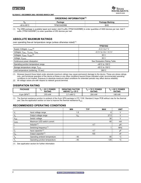
ABSOLUTE MAXIMUM RATINGS<br />
over operating free-air temperature range (unless otherwise noted) (1)<br />
DISSIPATION RATING<br />
RECOMMENDED OPERATING CONDITIONS<br />
ORDERING INFORMATION (1)<br />
T A Package Package Marking<br />
–40 to 85°C TPS61042DRB BHS<br />
www.ti.com<br />
(1) The DRB package is available taped and reeled. Add R suffix (TPS61042DRBR) to order quantities of 3000 devices per reel. Add T<br />
suffix (TPS61042DRBT) to order quantities of 250 devices per reel.<br />
TPS61042<br />
Supply Voltages, v (VIN) (2) –0.3 V to 7 V<br />
Voltages, V (Rs) , V (CTRL), V (FB)<br />
–0.3 V to Vin + 0.3 V<br />
Voltages, V (SW), V (<strong>LED</strong>) (2) 30 V<br />
Voltage, V (OVP)<br />
Continuous power dissipation See Dissipation Rating Table<br />
Operating junction temperature range –40°C to 150°C<br />
Storage temperature range, T STG<br />
30 V<br />
–65°C to 150°C<br />
Lead temperature (soldering, 10 sec) 260°C<br />
(1) Stresses beyond those listed under absolute maximum ratings may cause permanent damage to the device. These are stress ratings<br />
only, and functional operation of the device at these or any other conditions beyond those indicated under recommended operating<br />
conditions is not implied. Exposure to absolute-maximum-rated conditions for extended periods may affect device reliability.<br />
(2) All voltage values are with respect to network ground terminal.<br />
PACKAGE T A ≤ 25°C POWER DERATING FACTOR T A = 70°C POWER T A = 85°C POWER<br />
RATING ABOVE T A= 25°C RATING RATING<br />
8 pin QFN (1) 370 mW 3.7 mW/°C 204 mW 148 mW<br />
(1) The thermal resistance junction to ambient of the 8-pin QFN package is 270 °C/W. Standard 2-layer PCB without vias for the thermal<br />
pad. See the application section on how to improve the thermal resistance R θJA.<br />
MIN TYP MAX UNIT<br />
V I Input voltage range 1.8 6 V<br />
V s Output voltage range V IN 27.5 V<br />
V SW Switch voltage 30 V<br />
I (<strong>LED</strong>) Maximum <strong>LED</strong> switch current 60 mA<br />
L Inductor (1) 4.7 µH<br />
f Switching frequency (1) 1 MHz<br />
C I Input capacitor (1) 4.7 µF<br />
C O Output capacitor (1) 100 nF<br />
T A Operating ambient temperature –40 85 °C<br />
T J Operating junction temperature –40 125 °C<br />
(1) See application section for further information<br />
2 Submit Documentation Feedback