Constant Current LED Driver (Rev. C) - Educypedia
Constant Current LED Driver (Rev. C) - Educypedia
Constant Current LED Driver (Rev. C) - Educypedia

You also want an ePaper? Increase the reach of your titles
YUMPU automatically turns print PDFs into web optimized ePapers that Google loves.
www.ti.com<br />
FEATURES DESCRIPTION<br />
• <strong>Current</strong> Source With Overvoltage Protection The TPS61042 is a high frequency boost converter<br />
• Input Voltage Range . . 1.8 V to 6 V<br />
with constant current output that drives white <strong>LED</strong>s<br />
•<br />
•<br />
Internal 30 V Switch<br />
Up to 85% Efficiency<br />
or similar. The <strong>LED</strong> current is set with the external<br />
sense resistor (RS) and is directly regulated by the<br />
feedback pin (FB) that regulates the voltage across<br />
• Precise Brightness Control Using PWM Signal<br />
or Analog Signal<br />
the sense resistor RS to 252 mV (typ). To control<br />
<strong>LED</strong> brightness, the <strong>LED</strong> current can be pulsed by<br />
•<br />
•<br />
Switching Frequency . . Up to 1 MHz<br />
Internal Power MOSFET Switch . . 500 mA<br />
applying a PWM (pulse width modulated) signal with<br />
a frequency range of 100 Hz to 50 kHz to the control<br />
pin (CTRL). To allow higher flexibility, the device can<br />
• Operates With Small Output Capacitors Down be configured where the brightness can be controlled<br />
to 100 nF<br />
by an analog signal as well, as described in the<br />
•<br />
•<br />
Disconnects <strong>LED</strong>s During Shutdown<br />
No Load Quiescent <strong>Current</strong> . . 38 µA Typ<br />
application information section. To avoid possible<br />
leakage currents through the <strong>LED</strong>s during shutdown,<br />
the control pin (CTRL) disables the device and<br />
• Shutdown <strong>Current</strong> . . 0.1 µA Typ<br />
disconnects the <strong>LED</strong>s from ground. For maximum<br />
• Available in a Small 3 mm × 3 mm QFN<br />
Package<br />
safety during operation, the output has integrated<br />
overvoltage protection that prevents damage to the<br />
device in case of a high impedance output (e.g.<br />
APPLICATIONS<br />
faulty <strong>LED</strong>).<br />
• White <strong>LED</strong> Supply for Backlight/Sidelight<br />
Displays<br />
– PDA, Pocket PC, Smart Phones<br />
– Handheld Devices<br />
– Cellular Phones<br />
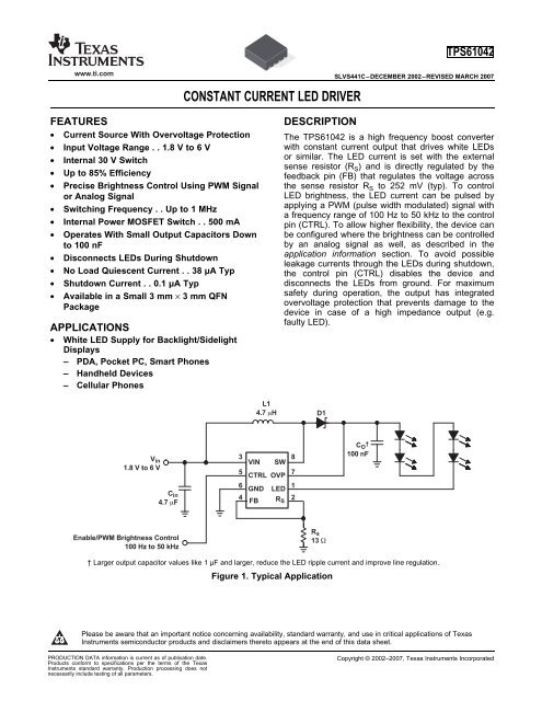
V in<br />
1.8 V to 6 V<br />
C in<br />
4.7 F<br />
Enable/PWM Brightness Control<br />
100 Hz to 50 kHz<br />
CONSTANT CURRENT <strong>LED</strong> DRIVER<br />
3<br />
5<br />
6<br />
4<br />
VIN<br />
L1<br />
4.7 H<br />
SW<br />
CTRL OVP<br />
GND<br />
FB<br />
<strong>LED</strong><br />
R S<br />
8<br />
7<br />
1<br />
2<br />
D1<br />
R s<br />
13 <br />
C O †<br />
100 nF<br />
TPS61042<br />
SLVS441C–DECEMBER 2002–REVISED MARCH 2007<br />
† Larger output capacitor values like 1 µF and larger, reduce the <strong>LED</strong> ripple current and improve line regulation.<br />
Figure 1. Typical Application<br />
Please be aware that an important notice concerning availability, standard warranty, and use in critical applications of Texas<br />
Instruments semiconductor products and disclaimers thereto appears at the end of this data sheet.<br />
PRODUCTION DATA information is current as of publication date. Copyright © 2002–2007, Texas Instruments Incorporated<br />
Products conform to specifications per the terms of the Texas<br />
Instruments standard warranty. Production processing does not<br />
necessarily include testing of all parameters.
TPS61042<br />
SLVS441C–DECEMBER 2002–REVISED MARCH 2007<br />
ABSOLUTE MAXIMUM RATINGS<br />
over operating free-air temperature range (unless otherwise noted) (1)<br />
DISSIPATION RATING<br />
RECOMMENDED OPERATING CONDITIONS<br />
ORDERING INFORMATION (1)<br />
T A Package Package Marking<br />
–40 to 85°C TPS61042DRB BHS<br />
www.ti.com<br />
(1) The DRB package is available taped and reeled. Add R suffix (TPS61042DRBR) to order quantities of 3000 devices per reel. Add T<br />
suffix (TPS61042DRBT) to order quantities of 250 devices per reel.<br />
TPS61042<br />
Supply Voltages, v (VIN) (2) –0.3 V to 7 V<br />
Voltages, V (Rs) , V (CTRL), V (FB)<br />
–0.3 V to Vin + 0.3 V<br />
Voltages, V (SW), V (<strong>LED</strong>) (2) 30 V<br />
Voltage, V (OVP)<br />
Continuous power dissipation See Dissipation Rating Table<br />
Operating junction temperature range –40°C to 150°C<br />
Storage temperature range, T STG<br />
30 V<br />
–65°C to 150°C<br />
Lead temperature (soldering, 10 sec) 260°C<br />
(1) Stresses beyond those listed under absolute maximum ratings may cause permanent damage to the device. These are stress ratings<br />
only, and functional operation of the device at these or any other conditions beyond those indicated under recommended operating<br />
conditions is not implied. Exposure to absolute-maximum-rated conditions for extended periods may affect device reliability.<br />
(2) All voltage values are with respect to network ground terminal.<br />
PACKAGE T A ≤ 25°C POWER DERATING FACTOR T A = 70°C POWER T A = 85°C POWER<br />
RATING ABOVE T A= 25°C RATING RATING<br />
8 pin QFN (1) 370 mW 3.7 mW/°C 204 mW 148 mW<br />
(1) The thermal resistance junction to ambient of the 8-pin QFN package is 270 °C/W. Standard 2-layer PCB without vias for the thermal<br />
pad. See the application section on how to improve the thermal resistance R θJA.<br />
MIN TYP MAX UNIT<br />
V I Input voltage range 1.8 6 V<br />
V s Output voltage range V IN 27.5 V<br />
V SW Switch voltage 30 V<br />
I (<strong>LED</strong>) Maximum <strong>LED</strong> switch current 60 mA<br />
L Inductor (1) 4.7 µH<br />
f Switching frequency (1) 1 MHz<br />
C I Input capacitor (1) 4.7 µF<br />
C O Output capacitor (1) 100 nF<br />
T A Operating ambient temperature –40 85 °C<br />
T J Operating junction temperature –40 125 °C<br />
(1) See application section for further information<br />
2 Submit Documentation Feedback
www.ti.com<br />
ELECTRICAL CHARACTERISTICS<br />
VI = 3.6 V, CTRL= VI , TA = -40°C to + 85°C , typical values are at TA = 25°C (unless otherwise noted)<br />
Supply current<br />
TPS61042<br />
SLVS441C–DECEMBER 2002–REVISED MARCH 2007<br />
PARAMETER TEST CONDITIONS MIN TYP MAX UNIT<br />
V I Input voltage range 1.8 6.0 V<br />
I (Q) Operating quiescent current into VIN I O = 0 mA, not switching 38 65 µA<br />
I O(sd) Shutdown current CTRL = GND 0.1 1 µA<br />
V UVLO Under-voltage lockout threshold V I falling 1.5 1.7 V<br />
CTRL<br />
V IH CTRL high level input voltage 1.3 V<br />
V IL CTRL low level input voltage 0.3 V<br />
I Ikg CTRL input leakage current CTRL = GND or VIN 0.1 µA<br />
t on Minimum CTRL pulse width to enable CTRL = low to high 50 us<br />
t off Minimum CTRL pulse width to disable CTRL = high to low 10 32 ms<br />
f (CTRL) PWM switching frequency applied to 0.1 50 kHz<br />
CTRL<br />
D (CTRL) PWM duty cycle applied to CTRL 1% 100%<br />
Power switch and current limit (SW)<br />
V S Maximum switch voltage 30 V<br />
r ds(ON) MOSFET on-resistance V I = 3.6 V; I (SW) = 200 mA 300 600 mΩ<br />
I lkg MOSFET leakage current V (SW) = 28 V 0.1 10 µA<br />
I LIM MOFSET current limit 400 500 600 mA<br />
<strong>LED</strong> switch and current limit (<strong>LED</strong>)<br />
V S Maximum switch voltage 30 V<br />
r ds(ON) MOSFET on-resistance V I = 3.6 V; I S = 20 mA 1 2 Ω<br />
I lkg MOSFET leakage current V (<strong>LED</strong>)= 28 V 0.1 10 µA<br />
Output<br />
V O Output voltage range V I 27.5 V<br />
I (FB) Feedback input bias current (1) V (FB) = 0.252 V 100 nA<br />
V FB Feedback trip point voltage 1.8 V ≤ V I≤ 6 V 244 252 260 mV<br />
V (OVP) Output overvoltage protection V O rising 27.5 29 30 V<br />
V hys(OVP) Output overvoltage protection hysteresis 5 7 V<br />
I (OVP) OVP input current V O = 15 V 9 12 µA<br />
(1) The feedback input is high impedance MOSFET Gate input.<br />
Submit Documentation Feedback<br />
3
TPS61042<br />
SLVS441C–DECEMBER 2002–REVISED MARCH 2007<br />
<strong>LED</strong><br />
1<br />
RS 2<br />
VIN 3<br />
FB 4<br />
The exposed thermal die pad is connected to GND.<br />
DRB PACKAGE<br />
(TOP VIEW)<br />
Exposed<br />
Thermal<br />
Die Pad<br />
Terminal Functions<br />
8<br />
7<br />
6<br />
5<br />
SW<br />
OVP<br />
GND<br />
CTRL<br />
TERMINAL NAME NO. I/O DESCRIPTION<br />
www.ti.com<br />
Combined enable and PWM control pin. If CTRL is constantly pulled high, the device is enabled and the<br />
CTRL 5 I internal <strong>LED</strong> switch (Q2) is constantly turned on. When CTRL is pulled to GND, the device is disabled.<br />
Apply a PWM signal (100 Hz to 50 kHz) to this pin to control the brightness of the <strong>LED</strong>s<br />
FB 4 I Feedback. FB regulates the <strong>LED</strong> current through the sense resistor by regulating the voltage across R S to<br />
252 mV.<br />
GND 6 GND<br />
<strong>LED</strong> 1 I Input of the <strong>LED</strong> switch (Q2). Connect the <strong>LED</strong>s to this pin.<br />
OVP 7 I Overvoltage protection. OVP is connected to the output capacitor of the converter.<br />
RS 2 O Output of the internal <strong>LED</strong> switch. The sense resistor that programs the <strong>LED</strong> current is connected to RS.<br />
SW 8 I Drain of the integrated switch (Q1)<br />
VIN 3 I Input supply pin.<br />
4 Submit Documentation Feedback
www.ti.com<br />
VIN<br />
CTRL<br />
GND<br />
FB<br />
EN<br />
UVLO<br />
Bias<br />
Thermal<br />
Shutdown<br />
Enable<br />
Control<br />
Logic<br />
PWM<br />
Gate<br />
Drive<br />
V REF<br />
–<br />
+<br />
EN<br />
V REF<br />
0.252 V<br />
EN<br />
Error<br />
Comparator<br />
FUNCTIONAL BLOCK DIAGRAM<br />
Control<br />
Logic<br />
Gate<br />
<strong>Driver</strong><br />
Overvoltage Protection<br />
400 ns Min<br />
Off Time<br />
Submit Documentation Feedback<br />
<strong>Current</strong><br />
Limit<br />
Softstart<br />
6 s Max<br />
On Time<br />
+<br />
–<br />
Q1<br />
0.4 V<br />
R1<br />
2 M<br />
R2<br />
30 k<br />
Q2<br />
TPS61042<br />
SLVS441C–DECEMBER 2002–REVISED MARCH 2007<br />
SW<br />
OVP<br />
<strong>LED</strong><br />
RS<br />
5
TPS61042<br />
SLVS441C–DECEMBER 2002–REVISED MARCH 2007<br />
η Efficiency<br />
Efficiency – %<br />
90<br />
88<br />
86<br />
84<br />
82<br />
80<br />
78<br />
76<br />
74<br />
72<br />
70<br />
V I = 4.2V<br />
V I = 3.6V<br />
V I = 2.4V<br />
4 <strong>LED</strong>s ≈ 13 V, C O = 1 μF<br />
0.1 1 10 100<br />
IO – Output <strong>Current</strong> – mA<br />
TYPICAL CHARACTERISTICS<br />
Table of Graphs<br />
Efficiency – %<br />
88<br />
86<br />
84<br />
82<br />
80<br />
78<br />
76<br />
74<br />
72<br />
70<br />
I O = 15 mA<br />
www.ti.com<br />
FIGURE<br />
vs <strong>LED</strong> current Figure 2<br />
vs Input voltage Figure 3<br />
I Q Operating Quiescent <strong>Current</strong> into VIN vs Input voltage and Temperature Figure 4<br />
V (FB) Feedback voltage vs Temperature Figure 5<br />
I (FB) Feedback current vs Temperature Figure 6<br />
r ds(on)<br />
Main switch Q1<br />
<strong>LED</strong> switch Q2<br />
vs Temperature Figure 7<br />
vs Input voltage Figure 8<br />
vs Temperature Figure 9<br />
vs Input voltage Figure 10<br />
I <strong>LED</strong> Average <strong>LED</strong> current vs PWM duty cycle on CTRL pin Figure 11<br />
Soft start Figure 12<br />
PFM operation (fixed peak current control) Figure 13<br />
Burst mode operation (fixed peak current Figure 14<br />
control)<br />
PWM dimming Figure 15<br />
Efficiency Efficiency<br />
vs vs<br />
<strong>LED</strong> <strong>Current</strong> Input Voltage<br />
4 <strong>LED</strong>s ≈ 13 V, C O = 1 μF<br />
1 2 3 4 5 6<br />
VI – Input Voltage – V<br />
Figure 2. Figure 3.<br />
6 Submit Documentation Feedback
www.ti.com<br />
Quiescent <strong>Current</strong> into V I/μA<br />
I (fb) - Feedback <strong>Current</strong> - nA<br />
r ds(on) − On-State Resistance − mΩ<br />
50<br />
45<br />
40<br />
35<br />
30<br />
25<br />
20<br />
15<br />
10<br />
5<br />
0<br />
60<br />
40<br />
20<br />
0<br />
-20<br />
-40<br />
-60<br />
600<br />
500<br />
400<br />
300<br />
200<br />
100<br />
0<br />
T A = 85°C<br />
T A = 25°C<br />
T A = -40°C<br />
1.8 2.4 3.0 3.6 4.2 4.8 5.4 6.0<br />
V CC = 5 V<br />
V I - Input Voltage - V<br />
V CC = 3.6 V<br />
V CC = 2.4 V<br />
-40 -15 10 35 60 85<br />
T A - Free-Air Temperature - °C<br />
1.8 2.4 3.0 3.6 4.2 4.8 5.4 6.0<br />
V I − Input Voltage − V<br />
T A = 27°C<br />
V (fb) - Feedback Voltage - mV<br />
r ds(on) − On-State Resistance − mΩ<br />
r ds(on) - On-State Resistance - Ω<br />
260<br />
258<br />
256<br />
254<br />
252<br />
250<br />
248<br />
246<br />
244<br />
242<br />
240<br />
500<br />
450<br />
400<br />
350<br />
300<br />
250<br />
200<br />
1.6<br />
1.5<br />
1.4<br />
1.3<br />
1.2<br />
1.1<br />
1.0<br />
0.9<br />
0.8<br />
0.7<br />
0.6<br />
V CC = 3.7 V<br />
-40 -15 10 35 60 85<br />
V CC = 3.6 V<br />
T A - Free-Air Temperature - °C<br />
−40 −15 10 35 60 85<br />
V CC = 3.6 V<br />
T A − Free-Air Temperature − °C<br />
-40 -15 10 35 60 85<br />
T A - Free-Air Temperature - °C<br />
TPS61042<br />
SLVS441C–DECEMBER 2002–REVISED MARCH 2007<br />
Operating Quiescent <strong>Current</strong> into VIN Feedback Voltage<br />
vs vs<br />
Input Voltage and Temperature Temperature<br />
Figure 4. Figure 5.<br />
Feedback <strong>Current</strong> r ds(on) Main Switch (Q1)<br />
vs vs<br />
Temperature Temperature<br />
Figure 6. Figure 7.<br />
r ds(ON) Main Switch (Q1) r ds(on) <strong>LED</strong> Switch (Q2)<br />
vs vs<br />
Input Voltage Temperature<br />
Figure 8. Figure 9.<br />
Submit Documentation Feedback<br />
7
TPS61042<br />
SLVS441C–DECEMBER 2002–REVISED MARCH 2007<br />
r ds(on) - On-State Resistance - Ω<br />
3.0<br />
2.5<br />
2.0<br />
1.5<br />
1.0<br />
0.5<br />
0.0<br />
V out<br />
10V/Div<br />
CTRL<br />
1V/Div<br />
Input <strong>Current</strong><br />
100mA/Div<br />
V sw<br />
5V/Div<br />
V out<br />
50mV/Div<br />
<strong>LED</strong> <strong>Current</strong><br />
20mA/Div<br />
r ds(on) <strong>LED</strong> Switch (Q2) Average <strong>LED</strong> <strong>Current</strong><br />
vs vs<br />
Input Voltage PWM Duty Cycle on CTRL Pin<br />
1.8 2.4 3.0 3.6 4.2 4.8 5.4 6.0<br />
V I - Input Voltage - V<br />
50s/Div<br />
2.5s/Div<br />
T A = 25°C<br />
I O - Output <strong>Current</strong> - mA<br />
20<br />
15<br />
10<br />
5<br />
0<br />
V sw<br />
5V/Div<br />
V out<br />
500mV/Div<br />
<strong>LED</strong> <strong>Current</strong><br />
20mA/Div<br />
V sw<br />
5V/Div<br />
V out<br />
500mV/Div<br />
<strong>LED</strong> <strong>Current</strong><br />
20mA/Div<br />
f PWM = 100 Hz f PWM = 50 kHz<br />
f PWM = 25 kHz<br />
www.ti.com<br />
0 20 40 60 80 100<br />
Duty Cycle - %<br />
Figure 10. Figure 11.<br />
Softstart PFM Operation<br />
2.5s/Div<br />
Figure 12. Figure 13.<br />
Bust Mode Operation PWM Dimming<br />
25s/Div<br />
Figure 14. Figure 15.<br />
8 Submit Documentation Feedback
www.ti.com<br />
Operation<br />
Boost Converter<br />
Peak <strong>Current</strong> Control (Boost Converter)<br />
Softstart<br />
I I <br />
P(typ) (LIM) V I<br />
100 ns<br />
L<br />
I 500 mA <br />
P(typ) V I<br />
100 ns<br />
L<br />
DETAI<strong>LED</strong> DESCRIPTION<br />
TPS61042<br />
SLVS441C–DECEMBER 2002–REVISED MARCH 2007<br />
The TPS61042 operates like a standard boost converter but regulates the voltage across the sense resistor (R S)<br />
instead of the output voltage. This gives an accurate regulated <strong>LED</strong> current independent of the input voltage and<br />
number of <strong>LED</strong>s connected. With integrated overvoltage protection (OVP) the TPS61042 is configured as a<br />
current source with overvoltage protection ideally suited to drive <strong>LED</strong>s. With the 30V internal switch, the device<br />
can generate output voltages of up to 27.5 V and has an internal 500mA MOSFET switch (Q1). This allows<br />
several <strong>LED</strong>s to be connected in series to the output. The internal <strong>LED</strong> switch (Q2) in series with the <strong>LED</strong>s has<br />
a maximum current rating of 60 mA and disconnects the <strong>LED</strong>s from ground during shutdown. The <strong>LED</strong> switch is<br />
driven by a PWM signal applied to the control pin (CTRL), which directly controls the <strong>LED</strong> brightness. With this<br />
control method the <strong>LED</strong> brightness depends on the PWM duty cycle only and is independent of the PWM<br />
frequency and amplitude.<br />
The boost converter operates in a pulse frequency modulation (PFM) scheme with constant peak current control.<br />
This control scheme maintains high efficiency over the entire load current range and with a switching frequency<br />
of up to 1 MHz, enables the use of small external components. The converter monitors the sense voltage across<br />
R S with the feedback pin (FB) and, when the feedback voltage falls below the reference voltage (252 mV typ),<br />
the main switch turns on and the current ramps up. The main switch turns off when the inductor current reaches<br />
the internally set peak current of 500 mA (typ). Refer to the peak current control section for more information.<br />
The second criteria that turns off the main switch is the maximum on-time of 6 µs (typ). This limits the maximum<br />
on-time of the converter in extreme conditions. As the switch is turned off the external Schottky diode is forward<br />
biased, delivering the stored inductor energy to the output. The main switch remains off until the minimum off<br />
time of 400 ns (typ) has passed and the feedback voltage is below the reference voltage again. Using this PFM<br />
peak current control scheme, the converter operates in discontinuous conduction mode (DCM) where the<br />
switching frequency depends on the inductor, input and output voltage, and <strong>LED</strong> current. Lower <strong>LED</strong> currents<br />
reduce the switching frequency, which results in high efficiency over the entire <strong>LED</strong> current range. This<br />
regulation scheme is inherently stable, allowing a wide range for the selection of the inductor and output<br />
capacitor.<br />
The internal switch is turned on until the inductor current reaches the DC current limit (I LIM) of 500 mA (typ) .<br />
Due to the internal current limit delay of 100 ns (typ) the actual current exceeds the DC current limit threshold by<br />
a small amount. The typical peak current limit can be calculated:<br />
The higher the input voltage and the lower the inductor value, the greater the current limit overshoot.<br />
All inductive step-up converters exhibit high in-rush current during start-up if no special precautions are taken.<br />
This can cause voltage drops at the input rail during start-up, which may result in an unwanted or premature<br />
system shutdown.<br />
The TPS61042 limits this in-rush current during start-up by increasing the current limit in two steps starting from<br />
I LIM/4 for 256 switch cycles to I LIM/2 for the next 256 switch cycles and then full current limit. See Figure 12 for<br />
typical start-up behavior.<br />
Submit Documentation Feedback<br />
9
TPS61042<br />
SLVS441C–DECEMBER 2002–REVISED MARCH 2007<br />
Control (CTRL)<br />
High<br />
Low<br />
Minimum<br />
On-Time<br />
to Enable<br />
the Device<br />
(50 s)<br />
DETAI<strong>LED</strong> DESCRIPTION (continued)<br />
t on<br />
t<br />
t p<br />
D = t p/t<br />
t off<br />
Minimum<br />
Off-Time<br />
to Disable<br />
the Device<br />
(32 ms)<br />
Applying a PWM Signal to the CTRL Pin with an On-Time tp≤2.5μs<br />
t on<br />
www.ti.com<br />
The CTRL pin serves two functions. One is the enable and disable of the device. The other is the PWM control<br />
of the internal <strong>LED</strong> switch (Q2). If no PWM signal is applied to the CTRL pin, then the CTRL pin can be used as<br />
a standard enable pin for the device. To enable the device, the CTRL pin must be pulled high for time period of<br />
at least 50 µs. The device starts with the Softstart cycle. Pulling the CTRL pin to GND for a time period ≥32 ms<br />
disables the device, disconnecting the <strong>LED</strong>s from GND by opening the <strong>LED</strong> switch (Q2) to avoid any <strong>LED</strong><br />
leakage current. See Figure 16 for the CTRL pin timing.<br />
The internal <strong>LED</strong> switch (Q2) is driven by the PWM signal when applied to the CTRL pin. Applying a PWM<br />
signal in the range of 100 Hz to 50 kHz allows the <strong>LED</strong> current to be pulsed with the duty cycle of the PWM<br />
signal. The CTRL pin accepts a PWM duty cycle from D = 1% to 100%. Duty cycles below 1% are also possible<br />
with the restriction that the device is forced into shutdown as the off time of the applied PWM signal exceeds 10<br />
ms.<br />
When a PWM signal is applied to the CTRL pin the <strong>LED</strong> switch (Q2) turns on immediately. The internal error<br />
comparator is disabled for 400 ns. This 400 ns delay time is required to establish the correct voltage level across<br />
the sense resistor R S after the <strong>LED</strong> switch (Q2) is closed.<br />
To achieve good <strong>LED</strong> current accuracy and linearity, the switching frequency of the converter must be higher<br />
than the PWM frequency applied to the CTRL pin.<br />
Figure 16. CTRL Timing Diagram<br />
The CTRL timing diagram is shown in Figure 16. To enable the device, the CTRL signal must be high for 50 µs.<br />
The PWM signal can then be applied with a pulse width (t p) greater or smaller than t ON. To force the device into<br />
shutdown mode, the CTRL signal must be low for at least 32 ms. Requiring the CTRL pin to be low for 32mS<br />
before the device enters shutdown allows for PWM dimming frequencies as low as 100 Hz. The device is<br />
enabled again when a CTRL signal is high for a period of 50 µs minimum. See Figure 11 for the PWM duty cycle<br />
versus <strong>LED</strong> current characteristic.<br />
This CTRL pin must be terminated.<br />
In such a case the on-time of the PWM signal, tp, must be >2.5μs until the softstart is completed. The softstart is<br />
completed after 512 switching cycles. To simply, estimate the softstart time, multiply the period of the PWM<br />
signal times 512, and add 50μs to it. For a 50-kHz signal this would be 10.3ms as a minimum softstart time<br />
period. After the softstart time is completed the PWM on time can be reduced to tp >400ns.<br />
10 Submit Documentation Feedback
www.ti.com<br />
Overvoltage Protection (OVP)<br />
Undervoltage Lockout<br />
Thermal Shutdown<br />
DETAI<strong>LED</strong> DESCRIPTION (continued)<br />
TPS61042<br />
SLVS441C–DECEMBER 2002–REVISED MARCH 2007<br />
As with any current source, the output voltage rises as the output impedance increases or is disconnected. To<br />
prevent the output voltage from exceeding the maximum main switch (Q1) voltage rating of 30 V, an overvoltage<br />
protection circuit is integrated. When the output voltage exceeds the OVP threshold voltage, (Q1) turns off. The<br />
converter switch remains off until the output voltage falls below the OVP threshold voltage. As long as the output<br />
voltage is below the OVP threshold the converter continues its normal operation, until the output voltage<br />
exceeds the OVP threshold again.<br />
An undervoltage lockout feature prevents mis-operation of the device at input voltages below 1.5 V (typ). As long<br />
as the input voltage is below the undervoltage threshold the device remains off, with the main MOSFET switch<br />
(Q1) and the <strong>LED</strong> switch (Q2) open.<br />
An internal thermal shutdown is implemented in the TPS61042 that shuts down the device if the typical junction<br />
temperature of 160°C is exceeded. If the device is in thermal shutdown mode, the main MOSFET switch (Q1)<br />
and the <strong>LED</strong> switch (Q2) are open.<br />
Submit Documentation Feedback<br />
11
TPS61042<br />
SLVS441C–DECEMBER 2002–REVISED MARCH 2007<br />
APPLICATION INFORMATION<br />
Inductor Selection, Maximum Load <strong>Current</strong>, and Switching Frequency<br />
Inductor fall time:<br />
ip L<br />
t <br />
fall Vout–Vin<br />
For tfall ≥ 400 ns<br />
ip Vin<br />
I <br />
load max 2Vout<br />
ip2 L Vin<br />
I <br />
load max (VoutVin) (2 ip L2 400 ns Vin)<br />
ip 500 mA Vin<br />
η = expected converter efficiency. Typically between 70% to 85%<br />
100 ns<br />
L<br />
www.ti.com<br />
The PFM peak current control scheme of the TPS61042 is inherently stable. The inductor value does not affect<br />
the stability of the regulator. The selection of the inductor together with the nominal <strong>LED</strong> current, input, and<br />
output voltage of the application determines the switching frequency of the converter.<br />
The first step is to calculate the maximum load current the converter can support using the selected inductor.<br />
The inductor value has less effect on the maximum available load current and is only of secondary order. A<br />
good inductor value to start with is 4.7 µH. Depending on the application, inductor values down to 1.0 µH can be<br />
used. The maximum inductor value is determined by the maximum on time of the switch of 6 µs (typ). The peak<br />
current limit of 500 mA (typ) must be reached within this 6 µs for proper operation. The maximum load current of<br />
the converter is determined at the operation point where the converter starts to enter the continuous conduction<br />
mode. The converter must always operate in discontinuous conduction mode to maintain regulation.<br />
Depending on the time period of the inductor current fall time being larger or smaller compared to the minimum<br />
off time of the converter (400ns typ), the maximum load current can be calculated.<br />
for t fall ≤ 400 ns<br />
with:<br />
L = selected inductor value<br />
(Peak inductor current as described in the peak current control section)<br />
The above formula contains the expected converter efficiency that allows calculating the expected maximum<br />
load current the converter can support. The efficiency can be taken out of the efficiency graphs shown in<br />
Figure 2 and Figure 3 or 80% can be used as an accurate estimation.<br />
fs(ILOAD) <br />
2 I V V V <br />
LOAD O I F<br />
I <br />
(LIM) Vin<br />
If the converter can support the desired <strong>LED</strong> current, the next step is to calculate the converter switching<br />
frequency at the operation point, which must be ≤1 MHz. Also the converter switching frequency should be much<br />
higher than the applied PWM frequency at the CTRL pin to avoid non-linear brightness control. Assuming the<br />
converter shows no double pulses or pulse bursts (Figure 13, Figure 14) on the switch node (SW) the switching<br />
frequency at the operation point can be calculated as:<br />
100 ns2 L<br />
L<br />
with:<br />
I (LIM) = minimum switch current limit (500 mA typ)<br />
L = selected inductor value<br />
I (LOAD) = nominal load or <strong>LED</strong> current<br />
V F = Rectifier diode forward voltage (typically 0.3 V)<br />
12 Submit Documentation Feedback
www.ti.com<br />
Output Capacitor Selection and Line Regulation<br />
V O I O<br />
C O<br />
<br />
<br />
APPLICATION INFORMATION (continued)<br />
I <br />
1 (LIM)<br />
<br />
f<br />
s(ILOAD)<br />
Vin<br />
100 ns L<br />
L<br />
V V V<br />
O F I<br />
<br />
<br />
<br />
I P ESR<br />
TPS61042<br />
SLVS441C–DECEMBER 2002–REVISED MARCH 2007<br />
The smaller the inductor value, the higher the switching frequency of the converter but the lower the efficiency.<br />
The selected inductor must have a saturation current that meets the maximum peak current of the converter as<br />
calculated in the peak current control section. Use the maximum value for I (LIM) (600mA) for this calculation.<br />
Another important inductor parameter is the DC resistance. The lower the DC resistance the higher the<br />
efficiency of the converter. See Table 1 and Figure 22 to Figure 27 for inductor selection.<br />
Table 1. Possible Inductor<br />
Inductor Value Component Supplier Size<br />
10 µH muRata LQH43CN100K01 4,5 mm×3,2 mm×2.6 mm<br />
4.7 µH muRata LQH32CN4R7M11 3,2 mm×2,5 mm×2,0 mm<br />
10 µH Coilcraft DO1605T-103MX 5,5 mm ×4,1 mm ×1,8 mm<br />
4.7 µH Sumida CDRH3D16-4R7 3,8 mm×3,8 mm×1,8 mm<br />
3.3 µH Sumida CMD4D11- 3R3 3,5 mm×5,3 mm×1,2 mm<br />
4.7 µH Sumida CMD4D11- 4R7 3,5 mm×5,3 mm×1,2 mm<br />
3.3 µH Sumida CMD4D11- 3R3 3,5 mm×5,3 mm×1,2 mm<br />
4.7 µH Coiltronics SD12-4R7 5,2 mm×5,2 mm×1,2 mm<br />
3.3 µH Coilcraft LPO1704-332M 6,6 mm×5,5 mm×1,0 mm<br />
4.7 µH Coilcraft LPO1704-472M 6,6 mm×5,5 mm×1,0 mm<br />
For better output voltage filtering, a low ESR output capacitor is recommended. Ceramic capacitors have a low<br />
ESR value, but depending on the application, tantalum capacitors can be used.<br />
The selection of the output capacitor value directly influences the output voltage ripple of the converter which<br />
also influences line regulation. The larger the output voltage ripple, the larger the line regulation, which means<br />
that the <strong>LED</strong> current changes if the input voltage changes. If a certain change in <strong>LED</strong> current gives a noticeable<br />
change in <strong>LED</strong> brightness, depends on the <strong>LED</strong> manufacturer and on the application. Applications requiring<br />
good line regulation ≤1%/V (typ) must use output capacitor values ≥1 µF.<br />
See Table 2 and Figure 22 to Figure 27 for the selection of the output capacitor.<br />
Assuming the converter does not show double pulses or pulse bursts on the switch node (SW), the output<br />
voltage ripple is calculated as (see Figure 13, Figure 14):<br />
with:<br />
I (LIM) = minimum switch current limit (400 mA typ)<br />
L = selected inductor value<br />
I (LOAD) = nominal load current<br />
f S = switching frequency at the nominal load current as calculated before.<br />
V F = rectifier diode forward voltage (0.3 V typ)<br />
C O = selected output capacitor<br />
ESR = output capacitor ESR value<br />
Submit Documentation Feedback<br />
13
TPS61042<br />
SLVS441C–DECEMBER 2002–REVISED MARCH 2007<br />
Input Capacitor Selection<br />
Diode Selection<br />
Efficiency<br />
V <strong>LED</strong> I <strong>LED</strong><br />
V I I I<br />
www.ti.com<br />
For good input voltage filtering, low ESR ceramic capacitors are recommended. A 4.7 µF ceramic input capacitor<br />
is sufficient for most applications. For better input voltage filtering the capacitor value can be increased. Refer to<br />
Table 2 and Figure 22 to Figure 27 for input capacitor selection.<br />
Table 2. Possible Input and Output Capacitors<br />
Capacitor Voltage rating Component Supplier Comments<br />
4.7 µF/X5R/0805 6.3 V Tayo Yuden JMK212BY475MG C I<br />
10 µF/X5R/0805 6.3 V Tayo Yuden JMK212BJ106MG C I<br />
100 nF Any C O<br />
220 nF Any C O<br />
470 nF Any C O<br />
1.0 µF/X7R/1206 25 V Tayo Yuden TMK316BJ105KL C O<br />
1.0 µF/X7R/1206 35 V Tayo Yuden GMK316BJ105KL C O<br />
4.7 µF/X5R/1210 25 V Tayo Yuden TMK325BJ475MG C O<br />
To achieve high efficiency, a Schottky diode must be used. The current rating of the diode must meet the peak<br />
current rating of the converter as it is calculated in the peak current control section. Use the maximum value for<br />
I (Lim) for this calculation. See Table 3 and Figure 22 to Figure 27 for the Schottky diode selection.<br />
Component Supplier <strong>Rev</strong>erse voltage<br />
ON Semiconductor MBR0530 30 V<br />
ON Semiconductor MBR0520 20 V<br />
Toshiba CRS02 30 V<br />
Zetex ZHCS400 40 V<br />
Table 3. Possible Diodes<br />
The overall efficiency of the application depends on the specific application conditions and mainly on the<br />
selection of the inductor. A lower inductor value increases the switching frequency and switching losses yielding<br />
in a lower efficiency. A lower inductor dc resistance has lower copper losses, giving a higher efficiency.<br />
Therefore, the efficiency can typically vary ±5% depending on the selected inductor. Figure 2 and Figure 3 can<br />
be used as a guideline for the application efficiency. These curves show the typical efficiency powering four<br />
<strong>LED</strong>s using a 4.7 µH inductor with just 1,2 mm height. The efficiency curve in Figure 2 and Figure 3 show the<br />
efficiency delivering the power to the <strong>LED</strong>s rather than the overall converter efficiency and is calculated as:<br />
14 Submit Documentation Feedback
www.ti.com<br />
Setting The <strong>LED</strong> <strong>Current</strong><br />
I <strong>LED</strong> V FB<br />
R S<br />
<br />
PWM<br />
Signal<br />
0.252 V<br />
R S<br />
R<br />
PWM<br />
100 Hz to 50 kHz<br />
C<br />
Optional Filter for the<br />
use of a PWM Signal<br />
VIN<br />
SW<br />
CTRL OVP<br />
GND<br />
FB<br />
Enable: CTRL = High<br />
Disable: CTRL = Low<br />
R2<br />
<strong>LED</strong><br />
RS<br />
V ADJ<br />
(Brightness Control)<br />
R s<br />
VIN<br />
SW<br />
CTRL OVP<br />
GND<br />
FB<br />
R1<br />
I1<br />
<strong>LED</strong><br />
RS<br />
R s<br />
V s<br />
TPS61042<br />
SLVS441C–DECEMBER 2002–REVISED MARCH 2007<br />
The converter regulates the <strong>LED</strong> current by regulating the voltage across the current sense resistor (R S). The<br />
voltage across the sense resistor is regulated to the internal reference voltage of V (FB) = 252 mV.<br />
The <strong>LED</strong> current can be calculated:<br />
Figure 17. Setting the <strong>LED</strong> <strong>Current</strong><br />
The current programming method is used when the brightness of the <strong>LED</strong>s is fixed or controlled by a PWM<br />
signal applied to the CTRL pin. When using a PWM signal on the CTRL pin, the <strong>LED</strong> brightness is only<br />
dependent on the PWM duty cycle, independent of the PWM frequency, or amplitude, which simplifies the<br />
system.<br />
Alternatively, an analog voltage can be used as well to control the <strong>LED</strong> brightness.<br />
Figure 18. Setting the <strong>LED</strong> <strong>Current</strong><br />
Submit Documentation Feedback<br />
15
TPS61042<br />
SLVS441C–DECEMBER 2002–REVISED MARCH 2007<br />
www.ti.com<br />
In Figure 18 the <strong>LED</strong> current is determined by the voltage applied to R2 (V (adj) ) and the selection of R1, R2 and<br />
the sense resistor (RS ). In this configuration, the <strong>LED</strong> current is linear controlled instead of pulsed as in the<br />
configuration before. To select the resistor values following steps are required.<br />
1. Select the voltage V (adjmax) to turn the <strong>LED</strong>s off. → V (adjmax) (e.g. 3.3 V)<br />
2. Select the voltage V (adjmin) to turn the <strong>LED</strong>s fully on. → V (adjmin) (e.g. 0.0 V)<br />
3. Select the maximum and minimum <strong>LED</strong> current IO(max) and IO(min) . → (e.g. IO(max) = 20 mA, IO(min) = 0 mA)<br />
4. Calculate R2 to achieve a feedback current in the range of I1 = 3 µA to 10 µA as the <strong>LED</strong>s are fully<br />
turned on:<br />
V V<br />
ref adj(min)<br />
R2 <br />
I1<br />
5. Calculation of R1<br />
I R2 V I R2 V<br />
O(max) adj(min) O(min) adj(max)<br />
R1 V <br />
ref V I V I V I V I<br />
adj(max) O(max) ref O(min) adj(min) O(min) ref O(max)<br />
6. Calculation of the sense voltage (V S ) at maximum <strong>LED</strong> current<br />
V V 1 <br />
S ref R1–<br />
R1<br />
R2 R2 V adj(min)<br />
7. Calculation of the required sense resistor (R S )<br />
R S V S<br />
I O(max)<br />
16 Submit Documentation Feedback
www.ti.com<br />
PWM Control With Separate Enable<br />
Layout Considerations<br />
Thermal Considerations<br />
PWM Brightness Control<br />
100 Hz to 50 kHz<br />
Enable (EN)<br />
PWM Brightness Control<br />
100 Hz to 50 kHz<br />
PWM Brightness Control<br />
100 Hz to 50 kHz<br />
Enable (EN)<br />
Enable (EN)<br />
VIN<br />
VIN<br />
SW<br />
CTRL OVP<br />
GND<br />
FB<br />
CTRL<br />
GND<br />
FB<br />
VIN<br />
SW<br />
OVP<br />
<strong>LED</strong><br />
R S<br />
<strong>LED</strong><br />
RS<br />
SW<br />
CTRL OVP<br />
GND<br />
FB<br />
<strong>LED</strong><br />
RS<br />
TPS61042<br />
SLVS441C–DECEMBER 2002–REVISED MARCH 2007<br />
The control pin (CTRL) combines the enable function as well as the PWM brightness control function in one pin.<br />
For some systems an independent enable function is required. One way to implement this is to use the<br />
brightness control configuration as shown in the previous section Figure 18.<br />
Other possible solutions are shown in Figure 19, Figure 20, Figure 21.<br />
Figure 19. Separate Enable and PWM Control Using a Schottky Diode<br />
Figure 20. Separate Enable and PWM Control Using a Transistor<br />
Figure 21. Separate Enable and PWM Control Using an AND Gate<br />
In all switching power supplies the layout is an important step in the design, especially at high peak currents and<br />
switching frequencies. If the layout is not carefully done, the regulator might show noise problems and duty cycle<br />
jitter.<br />
The input capacitor should be placed as close as possible to the input pin for good input voltage filtering. The<br />
inductor and diode must be placed as close as possible to the switch pin to minimize noise coupling into other<br />
circuits. Since the feedback pin and network is a high impedance circuit, the feedback network should be routed<br />
away from the inductor.<br />
The TPS61042 comes in a thermally enhanced QFN package. The package includes a thermal pad improving<br />
the thermal capabilities of the package. See the QFN/SON PCB Attachment application note (SLUA271).<br />
The thermal resistance junction to ambient R ΘJA of the QFN package greatly depends on the PCB layout. Using<br />
thermal vias and wide PCB traces improves the thermal resistance R ΘJA. Under normal operation conditions no<br />
PCB vias are required for the thermal pad. However, the thermal pad must be soldered to the PCB.<br />
Submit Documentation Feedback<br />
17
TPS61042<br />
SLVS441C–DECEMBER 2002–REVISED MARCH 2007<br />
VIN<br />
1.8 V to 6 V<br />
C (IN)<br />
4.7 F<br />
Enable/PWM Brightness<br />
Control 100 HZ to 50 kHz<br />
VIN<br />
1.8 V to 6 V<br />
C (IN)<br />
4.7 F<br />
Enable/PWM Brightness<br />
Control 100 HZ to 50 kHz<br />
L1<br />
4.7 H<br />
Coilcraft LPO1704–472<br />
VIN<br />
CTRL<br />
GND<br />
FB<br />
SW<br />
OVP<br />
<strong>LED</strong><br />
R S<br />
L1<br />
4.7 H<br />
SUMIDA CMD4D11<br />
VIN<br />
CTRL<br />
GND<br />
FB<br />
SW<br />
OVP<br />
<strong>LED</strong><br />
R S<br />
D1<br />
ZHCS400<br />
R S<br />
13 <br />
D1<br />
ZHCS400<br />
R S<br />
13 <br />
C O<br />
1 F<br />
C O<br />
4.7 F<br />
www.ti.com<br />
Figure 22. TPS61042 With 1,0 mm Total System Height. Efficiency = 82.7%@V I = 3.0 V/19 mA<br />
Figure 23. TPS61042 With Low <strong>LED</strong> Ripple <strong>Current</strong> and Higher Accuracy Using a 4.7 µF Output Capacitor<br />
18 Submit Documentation Feedback
www.ti.com<br />
VIN<br />
2.7 V to 6 V<br />
C (IN)<br />
4.7 F<br />
Enable/PWM Brightness<br />
Control 100 HZ to 50 kHz<br />
VIN<br />
2.7 V to 6 V<br />
C IN<br />
4.7 F<br />
Enable/PWM Brightness<br />
Control 100 HZ to 50 kHz<br />
L1<br />
Sumida CDRH3D16–6R8<br />
6.8 H<br />
VIN<br />
CTRL<br />
GND<br />
FB<br />
SW<br />
OVP<br />
<strong>LED</strong><br />
R S<br />
L1<br />
10.0H<br />
Coilcraft DO1605T–103MX<br />
VIN<br />
CTRL<br />
GND<br />
FB<br />
D1<br />
Zetex ZHCS400<br />
SW<br />
OVP<br />
<strong>LED</strong><br />
Rs<br />
R S<br />
13 <br />
R S<br />
6.5 <br />
C O<br />
1 F<br />
D1<br />
Zetex ZHCS400<br />
C O<br />
100 nF<br />
R1 R2<br />
30 30<br />
TPS61042<br />
SLVS441C–DECEMBER 2002–REVISED MARCH 2007<br />
Figure 24. TPS61042 Powering 6 <strong>LED</strong>s, Efficiency = 84%@V I = 3.6 V/19 mA<br />
Figure 25. TPS61042 Powering 8 <strong>LED</strong>s, Efficiency = 81%@V I = 3.6 V/18.6 mA<br />
Submit Documentation Feedback<br />
19
TPS61042<br />
SLVS441C–DECEMBER 2002–REVISED MARCH 2007<br />
V CC = 1.8 V to 6 V<br />
C (IN)<br />
4.7 F<br />
Analog Brightness Control<br />
3.3 V <strong>LED</strong> Off<br />
0 V I<strong>LED</strong> = 20 mA<br />
V CC = 1.8 V to 6 V<br />
3.3 V PWM Signal<br />
0 % <strong>LED</strong>s on<br />
100 % <strong>LED</strong>s Off<br />
C IN<br />
4.7 F<br />
R<br />
C<br />
R2<br />
120 k<br />
R2<br />
120 k<br />
L1<br />
4.7 H<br />
VIN<br />
CTRL<br />
GND<br />
FB<br />
R1<br />
10 k<br />
SW<br />
OVP<br />
<strong>LED</strong><br />
R S<br />
L1<br />
4.7 H<br />
VIN<br />
CTRL<br />
GND<br />
FB<br />
R1<br />
10 k<br />
SW<br />
OVP<br />
<strong>LED</strong><br />
R S<br />
D1<br />
ZHCS400<br />
R S<br />
13 <br />
D1<br />
ZHCS400<br />
R S<br />
13 <br />
C O<br />
100 nF<br />
Figure 26. Adjustable Brightness Control Using an Analog Voltage<br />
C O<br />
100 nF<br />
Figure 27. Alternative Adjustable Brightness Control Using PWM Signal<br />
20 Submit Documentation Feedback<br />
www.ti.com
PACKAGING INFORMATION<br />
Orderable Device Status (1)<br />
Package<br />
Type<br />
Package<br />
Drawing<br />
Pins Package<br />
Qty<br />
TPS61042DRBR ACTIVE SON DRB 8 3000 Green (RoHS &<br />
no Sb/Br)<br />
TPS61042DRBRG4 ACTIVE SON DRB 8 3000 Green (RoHS &<br />
no Sb/Br)<br />
TPS61042DRBT ACTIVE SON DRB 8 250 Green (RoHS &<br />
no Sb/Br)<br />
TPS61042DRBTG4 ACTIVE SON DRB 8 250 Green (RoHS &<br />
no Sb/Br)<br />
Eco Plan (2) Lead/Ball Finish MSL Peak Temp (3)<br />
CU NIPDAU Level-2-260C-1 YEAR<br />
CU NIPDAU Level-2-260C-1 YEAR<br />
CU NIPDAU Level-2-260C-1 YEAR<br />
CU NIPDAU Level-2-260C-1 YEAR<br />
(1) The marketing status values are defined as follows:<br />
ACTIVE: Product device recommended for new designs.<br />
LIFEBUY: TI has announced that the device will be discontinued, and a lifetime-buy period is in effect.<br />
NRND: Not recommended for new designs. Device is in production to support existing customers, but TI does not recommend using this part in<br />
a new design.<br />
PREVIEW: Device has been announced but is not in production. Samples may or may not be available.<br />
OBSOLETE: TI has discontinued the production of the device.<br />
(2) Eco Plan - The planned eco-friendly classification: Pb-Free (RoHS), Pb-Free (RoHS Exempt), or Green (RoHS & no Sb/Br) - please check<br />
http://www.ti.com/productcontent for the latest availability information and additional product content details.<br />
TBD: The Pb-Free/Green conversion plan has not been defined.<br />
Pb-Free (RoHS): TI's terms "Lead-Free" or "Pb-Free" mean semiconductor products that are compatible with the current RoHS requirements<br />
for all 6 substances, including the requirement that lead not exceed 0.1% by weight in homogeneous materials. Where designed to be soldered<br />
at high temperatures, TI Pb-Free products are suitable for use in specified lead-free processes.<br />
Pb-Free (RoHS Exempt): This component has a RoHS exemption for either 1) lead-based flip-chip solder bumps used between the die and<br />
package, or 2) lead-based die adhesive used between the die and leadframe. The component is otherwise considered Pb-Free (RoHS<br />
compatible) as defined above.<br />
Green (RoHS & no Sb/Br): TI defines "Green" to mean Pb-Free (RoHS compatible), and free of Bromine (Br) and Antimony (Sb) based flame<br />
retardants (Br or Sb do not exceed 0.1% by weight in homogeneous material)<br />
(3) MSL, Peak Temp. -- The Moisture Sensitivity Level rating according to the JEDEC industry standard classifications, and peak solder<br />
temperature.<br />
PACKAGE OPTION ADDENDUM<br />
www.ti.com 5-Mar-2007<br />
Important Information and Disclaimer:The information provided on this page represents TI's knowledge and belief as of the date that it is<br />
provided. TI bases its knowledge and belief on information provided by third parties, and makes no representation or warranty as to the<br />
accuracy of such information. Efforts are underway to better integrate information from third parties. TI has taken and continues to take<br />
reasonable steps to provide representative and accurate information but may not have conducted destructive testing or chemical analysis on<br />
incoming materials and chemicals. TI and TI suppliers consider certain information to be proprietary, and thus CAS numbers and other limited<br />
information may not be available for release.<br />
In no event shall TI's liability arising out of such information exceed the total purchase price of the TI part(s) at issue in this document sold by TI<br />
to Customer on an annual basis.<br />
Addendum-Page 1
TAPE AND REEL INFORMATION<br />
*All dimensions are nominal<br />
Device Package<br />
Type<br />
Package<br />
Drawing<br />
Pins SPQ Reel Reel<br />
Diameter Width<br />
(mm) W1 (mm)<br />
PACKAGE MATERIALS INFORMATION<br />
www.ti.com 11-Mar-2008<br />
A0 (mm) B0 (mm) K0 (mm) P1<br />
(mm)<br />
TPS61042DRBR SON DRB 8 3000 330.0 12.4 3.3 3.3 1.1 8.0 12.0 Q2<br />
TPS61042DRBT SON DRB 8 250 180.0 12.4 3.3 3.3 1.1 8.0 12.0 Q2<br />
Pack Materials-Page 1<br />
W<br />
(mm)<br />
Pin1<br />
Quadrant
*All dimensions are nominal<br />
PACKAGE MATERIALS INFORMATION<br />
www.ti.com 11-Mar-2008<br />
Device Package Type Package Drawing Pins SPQ Length (mm) Width (mm) Height (mm)<br />
TPS61042DRBR SON DRB 8 3000 346.0 346.0 29.0<br />
TPS61042DRBT SON DRB 8 250 190.5 212.7 31.8<br />
Pack Materials-Page 2
IMPORTANT NOTICE<br />
Texas Instruments Incorporated and its subsidiaries (TI) reserve the right to make corrections, modifications, enhancements, improvements,<br />
and other changes to its products and services at any time and to discontinue any product or service without notice. Customers should<br />
obtain the latest relevant information before placing orders and should verify that such information is current and complete. All products are<br />
sold subject to TI’s terms and conditions of sale supplied at the time of order acknowledgment.<br />
TI warrants performance of its hardware products to the specifications applicable at the time of sale in accordance with TI’s standard<br />
warranty. Testing and other quality control techniques are used to the extent TI deems necessary to support this warranty. Except where<br />
mandated by government requirements, testing of all parameters of each product is not necessarily performed.<br />
TI assumes no liability for applications assistance or customer product design. Customers are responsible for their products and<br />
applications using TI components. To minimize the risks associated with customer products and applications, customers should provide<br />
adequate design and operating safeguards.<br />
TI does not warrant or represent that any license, either express or implied, is granted under any TI patent right, copyright, mask work right,<br />
or other TI intellectual property right relating to any combination, machine, or process in which TI products or services are used. Information<br />
published by TI regarding third-party products or services does not constitute a license from TI to use such products or services or a<br />
warranty or endorsement thereof. Use of such information may require a license from a third party under the patents or other intellectual<br />
property of the third party, or a license from TI under the patents or other intellectual property of TI.<br />
Reproduction of TI information in TI data books or data sheets is permissible only if reproduction is without alteration and is accompanied<br />
by all associated warranties, conditions, limitations, and notices. Reproduction of this information with alteration is an unfair and deceptive<br />
business practice. TI is not responsible or liable for such altered documentation. Information of third parties may be subject to additional<br />
restrictions.<br />
Resale of TI products or services with statements different from or beyond the parameters stated by TI for that product or service voids all<br />
express and any implied warranties for the associated TI product or service and is an unfair and deceptive business practice. TI is not<br />
responsible or liable for any such statements.<br />
TI products are not authorized for use in safety-critical applications (such as life support) where a failure of the TI product would reasonably<br />
be expected to cause severe personal injury or death, unless officers of the parties have executed an agreement specifically governing<br />
such use. Buyers represent that they have all necessary expertise in the safety and regulatory ramifications of their applications, and<br />
acknowledge and agree that they are solely responsible for all legal, regulatory and safety-related requirements concerning their products<br />
and any use of TI products in such safety-critical applications, notwithstanding any applications-related information or support that may be<br />
provided by TI. Further, Buyers must fully indemnify TI and its representatives against any damages arising out of the use of TI products in<br />
such safety-critical applications.<br />
TI products are neither designed nor intended for use in military/aerospace applications or environments unless the TI products are<br />
specifically designated by TI as military-grade or "enhanced plastic." Only products designated by TI as military-grade meet military<br />
specifications. Buyers acknowledge and agree that any such use of TI products which TI has not designated as military-grade is solely at<br />
the Buyer's risk, and that they are solely responsible for compliance with all legal and regulatory requirements in connection with such use.<br />
TI products are neither designed nor intended for use in automotive applications or environments unless the specific TI products are<br />
designated by TI as compliant with ISO/TS 16949 requirements. Buyers acknowledge and agree that, if they use any non-designated<br />
products in automotive applications, TI will not be responsible for any failure to meet such requirements.<br />
Following are URLs where you can obtain information on other Texas Instruments products and application solutions:<br />
Products Applications<br />
Amplifiers amplifier.ti.com Audio www.ti.com/audio<br />
Data Converters dataconverter.ti.com Automotive www.ti.com/automotive<br />
DLP® Products www.dlp.com Communications and www.ti.com/communications<br />
Telecom<br />
DSP dsp.ti.com Computers and www.ti.com/computers<br />
Peripherals<br />
Clocks and Timers www.ti.com/clocks Consumer Electronics www.ti.com/consumer-apps<br />
Interface interface.ti.com Energy www.ti.com/energy<br />
Logic logic.ti.com Industrial www.ti.com/industrial<br />
Power Mgmt power.ti.com Medical www.ti.com/medical<br />
Microcontrollers microcontroller.ti.com Security www.ti.com/security<br />
RFID www.ti-rfid.com Space, Avionics & www.ti.com/space-avionics-defense<br />
Defense<br />
RF/IF and ZigBee® Solutions www.ti.com/lprf Video and Imaging www.ti.com/video<br />
Wireless www.ti.com/wireless-apps<br />
Mailing Address: Texas Instruments, Post Office Box 655303, Dallas, Texas 75265<br />
Copyright © 2010, Texas Instruments Incorporated